EP0638904A2 - Dual-port memory - Google Patents
Dual-port memory Download PDFInfo
- Publication number
- EP0638904A2 EP0638904A2 EP94410047A EP94410047A EP0638904A2 EP 0638904 A2 EP0638904 A2 EP 0638904A2 EP 94410047 A EP94410047 A EP 94410047A EP 94410047 A EP94410047 A EP 94410047A EP 0638904 A2 EP0638904 A2 EP 0638904A2
- Authority
- EP
- European Patent Office
- Prior art keywords
- output
- line
- cell
- read
- memory
- Prior art date
- Legal status (The legal status is an assumption and is not a legal conclusion. Google has not performed a legal analysis and makes no representation as to the accuracy of the status listed.)
- Granted
Links
Images


Classifications
-
- G—PHYSICS
- G11—INFORMATION STORAGE
- G11C—STATIC STORES
- G11C7/00—Arrangements for writing information into, or reading information out from, a digital store
- G11C7/10—Input/output [I/O] data interface arrangements, e.g. I/O data control circuits, I/O data buffers
- G11C7/1075—Input/output [I/O] data interface arrangements, e.g. I/O data control circuits, I/O data buffers for multiport memories each having random access ports and serial ports, e.g. video RAM
-
- G—PHYSICS
- G11—INFORMATION STORAGE
- G11C—STATIC STORES
- G11C11/00—Digital stores characterised by the use of particular electric or magnetic storage elements; Storage elements therefor
- G11C11/21—Digital stores characterised by the use of particular electric or magnetic storage elements; Storage elements therefor using electric elements
- G11C11/34—Digital stores characterised by the use of particular electric or magnetic storage elements; Storage elements therefor using electric elements using semiconductor devices
- G11C11/40—Digital stores characterised by the use of particular electric or magnetic storage elements; Storage elements therefor using electric elements using semiconductor devices using transistors
- G11C11/41—Digital stores characterised by the use of particular electric or magnetic storage elements; Storage elements therefor using electric elements using semiconductor devices using transistors forming static cells with positive feedback, i.e. cells not needing refreshing or charge regeneration, e.g. bistable multivibrator or Schmitt trigger
- G11C11/413—Auxiliary circuits, e.g. for addressing, decoding, driving, writing, sensing, timing or power reduction
- G11C11/417—Auxiliary circuits, e.g. for addressing, decoding, driving, writing, sensing, timing or power reduction for memory cells of the field-effect type
- G11C11/419—Read-write [R-W] circuits
-
- G—PHYSICS
- G11—INFORMATION STORAGE
- G11C—STATIC STORES
- G11C7/00—Arrangements for writing information into, or reading information out from, a digital store
-
- G—PHYSICS
- G11—INFORMATION STORAGE
- G11C—STATIC STORES
- G11C7/00—Arrangements for writing information into, or reading information out from, a digital store
- G11C7/10—Input/output [I/O] data interface arrangements, e.g. I/O data control circuits, I/O data buffers
- G11C7/1006—Data managing, e.g. manipulating data before writing or reading out, data bus switches or control circuits therefor
-
- G—PHYSICS
- G11—INFORMATION STORAGE
- G11C—STATIC STORES
- G11C8/00—Arrangements for selecting an address in a digital store
- G11C8/04—Arrangements for selecting an address in a digital store using a sequential addressing device, e.g. shift register, counter
-
- G—PHYSICS
- G11—INFORMATION STORAGE
- G11C—STATIC STORES
- G11C8/00—Arrangements for selecting an address in a digital store
- G11C8/16—Multiple access memory array, e.g. addressing one storage element via at least two independent addressing line groups
Definitions
- the present invention relates to dual-access memories, that is to say which comprise a separate input and output, and more particularly memories of the first-in / first-out (FIFO) type.
- dual-access memories that is to say which comprise a separate input and output, and more particularly memories of the first-in / first-out (FIFO) type.
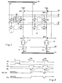
- FIG. 1 partially shows a conventional dual access memory structure.
- This memory comprises dual access memory cells 10 arranged in columns.
- each cell 10 comprises, for example, two inverters 10-1 arranged head to tail.
- Each inverter includes a pair of complementary output transistors (N and P channel MOS).
- the input and the output of the cell correspond respectively to the input and the output of a first of the inverters.
- the second inverter the output of which is connected to the input of the memory cell, includes more resistive output transistors than those of the first inverter, which limits the current consumption during a writing in the cell.
- Each column of cells is associated with an input line Bi and an output line Bo.
- the input of each cell 10 of a column is connected to the corresponding input line Bi by an N-channel MOS transistor M1.
- the output of each cell 10 of a column is connected to the corresponding output line Bo by an N channel MOS transistor M2.
- the gates of the transistors M1 of the same row of cells are connected to a writing line W and the gates of the transistors M2 of the same row of cells are connected to a reading line R.
- Each output line Bo is connected to a high supply potential Vdd by a P-channel MOS transistor MP1, called the precharge transistor.
- Each output line Bo is connected to an output Bo1 of the memory by successively an N-channel MOS transistor M3, a latch 12 consisting of inverters arranged head to tail, and a three-state gate 14.
- the transistors MP1 and M3 are controlled by a column reading signal RC.
- the three-state doors 14 are controlled by a validation signal EN which, as the case may be, is equal to the signal RC or fixed by an external device, such as a microprocessor, which reads the memory.
- the MP1 preload transistors can also be N-channel; in this case they are controlled by the logical inverse of the RC signal.
- the input lines Bi are connected directly, or via follower amplifiers not shown, to respective lines of an input data bus Di.
- the outputs Bo1 of the memory are connected to the respective lines of an output bus Do.
- data buses Di and Do of n lines, dual access memories of n columns are associated.
- the write W and read R lines are controlled by an address decoder, not shown.
- a device managing the input bus Di presents data on the bus Di, transmits an address (on an address bus not shown) which selects one of the rows of cells, and activates a line WC column writing (not shown in Figure 1).
- a device which manages the Do bus sends an address which selects one of the rows of cells, activates the line RC for reading columns, and validates the line EN.
- the dual-access memories of the type of FIG. 1 are often used in first-in / first-out (FIFO) type memories.
- a FIFO memory does not include an address bus.
- the column reading line RC is activated and the data that the memory then presents on its output (Bo1) is recovered.
- the WC column write line is activated by presenting data at its input (Bi).
- a FIFO memory generally comprises a dual access memory of the type of FIG. 1 with its address decoder, the addresses being supplied by a relatively complex control circuit which manages the "first-in / first-out" mechanism. depending on the WC read and RC column write signals, supplied from outside.
- FIG. 2 represents the appearance of various signals of the structure of FIG. 1 during the successive reading of a "0" in a first cell and twice a "1" in a second cell. At successive times t1, t2 and t3, it is decided to carry out the abovementioned readings.
- the column reading line RC and a line R1 which corresponds to one of the reading lines R are activated.
- the transistor MP2 is turned on and transmits the output of cell 10 on the output line Bo.
- the transistor MP1 is blocked and the line Bo is not forced to the potential Vdd.
- the cell 10 read stores a "0", which means that the input of the cell is at "0" while its output is at "1".
- line Bo remains at "1”.
- the transistor M3 is turned on and transmits the state "1" of the line Bo on the input of the latch 12 which reverses this state.
- the output Bo1, and the corresponding line of the bus Do pass or remain at "0".
- the lines RC and R1 are deactivated before time t2, which makes the precharge transistors MP1 conductive and blocks the output transistors M3.
- An object of the present invention is to provide a dual access memory structure having a particularly low consumption.
- Another object of the present invention is to provide a FIFO memory with particularly low consumption and of particularly simple structure.
- a dual-access memory comprising dual-access memory cells arranged in columns.
- One output line per column is connected to each cell of the column by a read transistor controlled by a respective read line.
- Precharge transistors connect the output lines to a precharge potential corresponding to a first logic state, these transistors being controlled by an inactive state of a read selection signal.
- Output transistors connect the output lines to an output of the memory.
- a false memory cell is associated with a false output line and a precharge transistor, the output of this false cell being in a second logic state opposite to said first logic state.
- a false read transistor is controlled by the active state of the read selection signal and connects the output of the false cell to the false output line. Means are provided for controlling said output transistors when the state of the false output line reaches a predetermined threshold between said first and second logic states.
- one entry line per column is connected to each cell of the column by a writing transistor controlled by a respective writing line.
- the memory includes, for each write line, a transistor connecting this write line to an input of the memory and controlled by the active state of a write select signal.
- the means for controlling the output transistors comprise a logic gate, a first input of which is connected to the false output line by means of an inverter and of which a second input receives the signal selection in reading.
- the false cell comprises a conductive transistor connected to a fixed potential corresponding to said second logic state.
- the memory is a first-in / first-out type memory comprising: a first looped shift register whose outputs respectively control the read lines, the shift of this register being controlled by the inverse of the read selection signal; and a second looped shift register, the outputs of which respectively control said write lines, the shift of this register being controlled by the inverse of the write selection signal.
- FIG. 3 the same elements as in FIG. 1 are designated by the same references.
- a false memory cell 10 ′ is provided for all of the columns of cells, the output of this false cell being connected to a false output line Bo ′ by an N channel MOS transistor M2 ′.
- the output of this false cell 10 ' is permanently fixed at "0" by an N-channel MOS transistor 10-2, connected between the transistor M2' and the ground, and the gate of which is connected to the potential Vdd.
- the transistors M2 'and 10-2 are chosen with the same characteristics, respectively, as the transistors M2 and the N-channel output transistor of a memory cell.
- the false output line Bo ' is connected to the potential Vdd, like the other output lines Bo, by a precharge transistor MP1, the gate of which is controlled by the column read signal RC. Unlike the read transistors M2, the gate of the transistor M2 'for reading the false cell is connected to the line RC.
- the gates of the output transistors M3, instead of being connected to the line RC, are connected to a line RC2 connected to the output of an AND gate 16.
- a first input of the AND gate 16 is connected to the line RC and the other to the false output line Bo 'via an inverter 18.
- FIG. 4 represents the appearance of various signals from the memory of FIG. 3 when a "1" is read in a memory cell while a "1" has previously been read in a cell of the same column. This case corresponds to the instant t3 of FIG. 2 where the output of a conventional memory presented an untimely transition to "0".
- the lines R and RC are activated.
- the preload transistors MP1 are blocked, the transistor M2 'and the transistor M2 of the cell to be read become conducting.
- the output of the false cell 10 'and the output of the cell 10 to be read are at "0", which causes, as shown, a progressive and synchronous discharge of the output lines Bo and Bo'.
- the threshold voltage Vt of the inverter 18 is not reached; the output of gate 16 remains at "0" and the output transistors M3 remain blocked.
- This first phase corresponds to the interval where the output of a conventional memory has an untimely transition to "0", as shown in dotted lines for the output Bo1.
- This inadvertent change to "0" is avoided, according to the invention, thanks to the fact that the output transistors M3 remain blocked during this first phase.
- each input line Bi is connected to the input of the memory by an N-channel MOS transistor M4.
- the gates of the M4 transistors are connected to a WC column writing line.
- the WC line is a line which is used to select the write memory; it is active at the same time as any of the writing lines W.
- FIG. 5 represents an embodiment of a circuit for controlling the write W and read R lines, making it possible, using a dual-access memory, to produce a FIFO memory of particularly simple structure.
- FIG. 5 illustrates an example where there are six reading lines R and six writing lines W.
- a circuit of the type of FIG. 5 is associated with the six reading lines R and another identical circuit is associated with the six lines writing W. We only describe below the control circuit associated with the reading lines.
- This control circuit includes a shift register with six flip-flops 20 arranged in cascade, that is to say that the output of each flip-flop is connected to the input of the next flip-flop.
- Each output of a flip-flop 20 is supplied to one of the reading lines R by an AND gate 22.
- a second input of AND doors 22 is connected to the column reading line RC which is also connected to the clock inputs of the flip-flops 20 via an inverter 24.
- a initialization signal RST is supplied to each of the flip-flops 20. Activation of this RST signal sets the first flip-flop 20 to "1" and all the others to "0".
- the shift register is looped back, that is to say that the output of the last flip-flop is connected to the input of the first flip-flop.
- the flip-flops 20 are arranged in an interlaced manner, that is to say that the flip-flop of last row (6) is disposed between the flip-flops of first row (1) and second row (2), that the penultimate penultimate row (5) is disposed between the second row (2) and third row (3) scales ...
- the connections between the scales are all of substantially the same length, whatever the number of flip-flops, which prevents the flip-flops from having different switching times.
- the flip-flop of rank 1 is at "1" and all the others at "0".
- the RC line is activated, the first row of cells is selected for reading.
- the RC line is deactivated, the "1" which was in the first flip-flop propagates in the second flip-flop.
- the second row of cells is selected for reading.
- the "1" reaches the last flip-flop (6), it returns to the first flip-flop as soon as the RC signal is deactivated.
- a control circuit identical to that of FIG. 5 is also associated with the writing lines W.
- the writing lines W are connected to the outputs of the AND gates 22 and the column writing line WC is connected to the input of the inverter 24.
- the ranks of the flip-flops can be changed if one wishes to read the stored data in an order different from that of their writing.
- a particularly simple FIFO memory structure is thus obtained since the rows of cells are directly selected by the shift registers without the need to use a conventional complex system for generating addresses and decoding these addresses.
- the devices which write or read in the FIFO memory can know the filling state of the latter. For this, these devices need a FULL signal indicating that the memory is full and possibly a 1 ⁇ 2FULL signal indicating that the memory is half full.
- FIG. 6 schematically represents a circuit making it possible to obtain such FULL and 1 ⁇ 2FULL signals.
- This circuit includes two counters per L 30 and 32, L being the number of rows of cells of the FIFO memory (6 in the example of FIG. 5).
- the counter 30 is activated by the column write line WC and the counter 32 is activated by the column read line RC.
- the two counters 30 and 32 are reset to zero by the signal RST.
- the outputs of the counters 30 and 32 are supplied to a digital subtractor 34 which provides the difference between the content of the counter 30 and that of the counter 32 (i.e. the difference between the number of written data and the number of data read).
- the output of the subtractor 34 is supplied to an input a of two comparators 36 and 38.
- An input b of the comparator 36 receives the number L-1 and an input b of the comparator 38 receives the number L / 2.
- the comparator 36 provides the full signal FULL when the result of the subtraction in the subtractor 34 is equal to L-1 and the comparator 38 activates the half-full state signal 1 ⁇ 2FULL when the result of the sub
Landscapes
- Engineering & Computer Science (AREA)
- Microelectronics & Electronic Packaging (AREA)
- Multimedia (AREA)
- Computer Hardware Design (AREA)
- Static Random-Access Memory (AREA)
Abstract
Description
La présente invention concerne les mémoires à double accès, c'est-à-dire qui comprennent une entrée et une sortie distinctes, et plus particulièrement les mémoires de type premier-entré/premier-sorti (FIFO).The present invention relates to dual-access memories, that is to say which comprise a separate input and output, and more particularly memories of the first-in / first-out (FIFO) type.
La figure 1 représente partiellement une structure de mémoire double accès classique. Cette mémoire comprend des cellules mémoire à double accès 10 disposées par colonnes. Comme cela est représenté, chaque cellule 10 comprend, par exemple, deux inverseurs 10-1 disposés tête-bêche. Chaque inverseur comprend une paire de transistors de sortie complémentaires (MOS à canaux N et P). L'entrée et la sortie de la cellule correspondent respectivement à l'entrée et à la sortie d'un premier des inverseurs. Le deuxième inverseur, dont la sortie est reliée à l'entrée de la cellule mémoire, comprend des transistors de sortie plus résistifs que ceux du premier inverseur, ce qui limite la consommation de courant lors d'une écriture dans la cellule.Figure 1 partially shows a conventional dual access memory structure. This memory comprises dual
A chaque colonne de cellules est associée une ligne d'entrée Bi et une ligne de sortie Bo. L'entrée de chaque cellule 10 d'une colonne est reliée à la ligne d'entrée correspondante Bi par un transistor MOS à canal N M1. La sortie de chaque cellule 10 d'une colonne est reliée à la ligne de sortie Bo correspondante par un transistor MOS à canal N M2. Les grilles des transistors M1 d'une même rangée de cellules sont reliées à une ligne d'écriture W et les grilles des transistors M2 d'une même rangée de cellules sont reliées à une ligne de lecture R.Each column of cells is associated with an input line Bi and an output line Bo. The input of each
Chaque ligne de sortie Bo est reliée à un potentiel d'alimentation haut Vdd par un transistor MOS à canal P MP1, dit transistor de précharge. Chaque ligne de sortie Bo est reliée à une sortie Bo1 de la mémoire par sucoessivement un transistor MOS à canal N M3, un verrou 12 constitué d'inverseurs disposés tête-bêche, et une porte trois états 14.Each output line Bo is connected to a high supply potential Vdd by a P-channel MOS transistor MP1, called the precharge transistor. Each output line Bo is connected to an output Bo1 of the memory by successively an N-channel MOS transistor M3, a
Les transistors MP1 et M3 sont commandés par un signal RC de lecture de colonne. Les portes trois états 14 sont commandées par un signal de validation EN qui, selon le cas, est égal au signal RC ou fixé par un dispositif externe, tel qu'un microprocesseur, qui lit la mémoire. Les transistors de précharge MP1 peuvent aussi être à canal N ; dans ce cas ils sont commandés par l'inverse logique du signal RC.The transistors MP1 and M3 are controlled by a column reading signal RC. The three-
Dans une configuration classique courante, les lignes d'entrée Bi sont reliées directement, ou par l'intermédiaire d'amplificateurs suiveurs non représentés, à des lignes respectives d'un bus de données d'entrée Di. Les sorties Bo1 de la mémoire sont reliées aux lignes respectives d'un bus de sortie Do. Ainsi, à des bus de données Di et Do de n lignes, on associe des mémoires à double accès de n colonnes.In a current conventional configuration, the input lines Bi are connected directly, or via follower amplifiers not shown, to respective lines of an input data bus Di. The outputs Bo1 of the memory are connected to the respective lines of an output bus Do. Thus, data buses Di and Do of n lines, dual access memories of n columns are associated.
Les lignes d'écriture W et de lecture R sont commandées par un décodeur d'adresses non représenté. Pour écrire dans la mémoire, un dispositif gérant le bus d'entrée Di présente une donnée sur le bus Di, émet une adresse (sur un bus d'adresses non représenté) qui sélectionne l'une des rangées de cellules, et active une ligne d'écriture de colonne WC (non représentée à la figure 1).The write W and read R lines are controlled by an address decoder, not shown. To write to the memory, a device managing the input bus Di presents data on the bus Di, transmits an address (on an address bus not shown) which selects one of the rows of cells, and activates a line WC column writing (not shown in Figure 1).
Pour lire dans la mémoire, un dispositif qui gère le bus Do émet une adresse qui sélectionne l'une des rangées de cellules, active la ligne RC de lecture de colonne, et valide la ligne EN.To read from the memory, a device which manages the Do bus sends an address which selects one of the rows of cells, activates the line RC for reading columns, and validates the line EN.
Les mémoires à double accès du type de la figure 1 sont souvent utilisées dans des mémoires de type premier-entré/premier-sorti (FIFO). Une mémoire FIFO ne comprend pas de bus d'adresses. Pour lire dans une mémoire FIFO, on active la ligne RC de lecture de colonne et on récupère la donnée que la mémoire présente alors sur sa sortie (Bo1). Pour écrire dans la mémoire FIFO, on active la ligne WC d'écriture de colonne en présentant une donnée à son entrée (Bi).The dual-access memories of the type of FIG. 1 are often used in first-in / first-out (FIFO) type memories. A FIFO memory does not include an address bus. To read from a FIFO memory, the column reading line RC is activated and the data that the memory then presents on its output (Bo1) is recovered. To write to the FIFO memory, the WC column write line is activated by presenting data at its input (Bi).
Une mémoire FIFO comprend généralement une mémoire à double accès du type de la figure 1 avec son décodeur d'adresses, les adresses étant fournies par un circuit de commande, relativement complexe, qui gère le mécanisme du "premier-entré/premier-sorti" en fonction des signaux de lecture WC et d'écriture RC de colonne, fournis de l'extérieur.A FIFO memory generally comprises a dual access memory of the type of FIG. 1 with its address decoder, the addresses being supplied by a relatively complex control circuit which manages the "first-in / first-out" mechanism. depending on the WC read and RC column write signals, supplied from outside.
La figure 2 représente l'allure de divers signaux de la structure de la figure 1 lors de la lecture successive d'un "0" dans une première cellule et de deux fois un "1" dans une deuxième cellule. A des instants t1, t2 et t3 successifs, on décide d'effectuer les lectures susmentionnées.FIG. 2 represents the appearance of various signals of the structure of FIG. 1 during the successive reading of a "0" in a first cell and twice a "1" in a second cell. At successive times t1, t2 and t3, it is decided to carry out the abovementioned readings.
A l'instant t1, on active la ligne de lecture de colonne RC et une ligne R1 qui correspond à l'une des lignes de lecture R. Le transistor MP2 est rendu passant et transmet la sortie de la cellule 10 sur la ligne de sortie Bo. Le transistor MP1 est bloqué et la ligne Bo n'est pas forcée au potentiel Vdd. La cellule 10 lue stocke un "0", ce qui veut dire que l'entrée de la cellule est à "0" alors que sa sortie est à "1". Ainsi, la ligne Bo reste à "1". Le transistor M3 est rendu passant et transmet l'état "1" de la ligne Bo sur l'entrée du verrou 12 qui inverse cet état. Ainsi, la sortie Bo1, et la ligne correspondante du bus Do, passent ou restent à "0". Les lignes RC et R1 sont désactivées avant l'instant t2, ce qui rend conducteurs les transistors de précharge MP1 et bloque les transistors de sortie M3.At time t1, the column reading line RC and a line R1 which corresponds to one of the reading lines R are activated. The transistor MP2 is turned on and transmits the output of
A l'instant t2, on décide de lire un "1" dans une deuxième cellule mémoire. La ligne RC est de nouveau activée et l'on active une ligne R2 correspondant à une autre ligne de lecture R. Cette fois-ci, la sortie de la cellule 10 lue est à "0". La ligne Bo passe lentement de Vdd à 0 en se déchargeant vers la sortie de la cellule 10 par le transistor M2, la sortie de la cellule 10 étant forcée à la masse par un transistor de la cellule. Le verrou 12 ne bascule que quand l'état de la ligne Bo atteint un seuil de basculement Vt à un instant t2s. Ainsi, la sortie Bo1 passe à "1" avec un certain retard par rapport à l'instant t2. Avant l'instant t3, les lignes RC et R2 sont désactivées, ce qui entraîne la remise à "1" des lignes de sortie Bo.At time t2, it is decided to read a "1" in a second memory cell. The line RC is activated again and a line R2 corresponding to another reading line R is activated. This time, the output of the
A l'instant t3, on lit la même cellule qu'à l'instant t2. Les lignes RC et R2 sont de nouveau activées. Comme à l'instant t2, la ligne Bo passe progressivement de Vdd à 0 en se déchargeant par le transistor M2 vers la sortie de la cellule lue. Toutefois, entre l'instant t3 et l'instant t3s où l'état de la ligne Bo atteint la tension seuil Vt, le verrou 12, dont l'entrée était à 0, bascule à l'instant t3, et bascule de nouveau à l'instant t3s. Ceci entraîne, comme cela est représenté, un passage intempestif à "0" de la sortie Bo1 entre les instants t3 et t3s.At time t3, we read the same cell as at time t2. The lines RC and R2 are activated again. As at time t2, the line Bo progressively goes from Vdd to 0 by discharging through the transistor M2 towards the output of the cell read. However, between the instant t3 and the instant t3s when the state of the line Bo reaches the threshold voltage Vt, the
On a également représenté, sous la référence Bix, l'allure d'une ligne d'entrée d'une deuxième mémoire à double accès dont l'entrée serait reliée au bus Do. L'état de cette ligne Bix varie de la même manière que la sortie correspondante Bo1.Also shown, under the reference Bi x , is the appearance of an input line of a second dual-access memory, the input of which would be connected to the bus Do. The state of this line Bi x varies in the same way as the corresponding output Bo1.
Une mémoire du type de la figure 1, comme tout circuit CMOS, ne consomme du courant que lors des transitions des signaux qui y transitent. Ainsi, la consommation d'une telle mémoire est indûment augmentée du fait des passages à "0" intempestifs de la sortie Do1 entre deux lectures d'un "1". La consommation est en outre d'autant plus grande que les lignes sur lesquelles transitent ces signaux sont longues. Ainsi, la consommation devient particulièrement importante si la sortie d'une première mémoire à double accès est reliée aux entrées de plusieurs autres mémoires à double accès.A memory of the type of FIG. 1, like any CMOS circuit, consumes current only during the transitions of the signals which pass through it. So the consumption of such memory is unduly increased due to untimely passing to "0" of the output Do1 between two readings of a "1". Consumption is also greater the longer the lines on which these signals pass. Thus, consumption becomes particularly significant if the output of a first dual-access memory is connected to the inputs of several other dual-access memories.
Un objet de la présente invention est de prévoir une structure de mémoire à double accès présentant une consommation particulièrement faible.An object of the present invention is to provide a dual access memory structure having a particularly low consumption.
Un autre objet de la présente invention est de prévoir une mémoire FIFO à consommation particulièrement faible et de structure particulièrement simple.Another object of the present invention is to provide a FIFO memory with particularly low consumption and of particularly simple structure.
Ces objets sont atteints grâce à une mémoire à double accès comprenant des cellules mémoire à double accès disposées en colonnes. Une ligne de sortie par colonne est reliée à chaque cellule de la colonne par un transistor de lecture commandé par une ligne de lecture respective. Des transistors de précharge relient les lignes de sortie à un potentiel de précharge correspondant à un premier état logique, ces transistors étant commandés par un état inactif d'un signal de sélection en lecture. Des transistors de sortie relient les lignes de sortie à une sortie de la mémoire. Une fausse cellule mémoire est associée à une fausse ligne de sortie et à un transistor de précharge, la sortie de cette fausse cellule étant à un deuxième état logique opposé audit premier état logique. Un faux transistor de lecture est commandé par l'état actif du signal de sélection en lecture et relie la sortie de la fausse cellule à la fausse ligne de sortie. Des moyens sont prévus pour commander lesdits transistors de sortie lorsque l'état de la fausse ligne de sortie atteint un seuil prédéterminé entre lesdits premier et deuxième états logiques.These objects are achieved thanks to a dual-access memory comprising dual-access memory cells arranged in columns. One output line per column is connected to each cell of the column by a read transistor controlled by a respective read line. Precharge transistors connect the output lines to a precharge potential corresponding to a first logic state, these transistors being controlled by an inactive state of a read selection signal. Output transistors connect the output lines to an output of the memory. A false memory cell is associated with a false output line and a precharge transistor, the output of this false cell being in a second logic state opposite to said first logic state. A false read transistor is controlled by the active state of the read selection signal and connects the output of the false cell to the false output line. Means are provided for controlling said output transistors when the state of the false output line reaches a predetermined threshold between said first and second logic states.
Selon un mode de réalisation de la présente invention, une ligne d'entrée par colonne est reliée à chaque cellule de la colonne par un transistor d'écriture commandé par une ligne d'écriture respective. La mémoire comprend, pour chaque ligne d'écriture, un transistor reliant cette ligne d'écriture à une entrée de la mémoire et commandé par l'état actif d'un signal de sélection en écriture.According to an embodiment of the present invention, one entry line per column is connected to each cell of the column by a writing transistor controlled by a respective writing line. The memory includes, for each write line, a transistor connecting this write line to an input of the memory and controlled by the active state of a write select signal.
Selon un mode de réalisation de la présente invention, les moyens pour commander les transistors de sortie comprennent une porte logique dont une première entrée est reliée à la fausse ligne de sortie par l'intermédiaire d'un inverseur et dont une deuxième entrée reçoit le signal de sélection en lecture.According to an embodiment of the present invention, the means for controlling the output transistors comprise a logic gate, a first input of which is connected to the false output line by means of an inverter and of which a second input receives the signal selection in reading.
Selon un mode de réalisation de la présente invention, la fausse cellule comprend un transistor conducteur relié à un potentiel fixe correspondant audit deuxième état logique.According to an embodiment of the present invention, the false cell comprises a conductive transistor connected to a fixed potential corresponding to said second logic state.
Selon un mode de réalisation de la présente invention, la mémoire est une mémoire de type premier-entrée/premier-sorti comprenant : un premier registre à décalage rebouclé dont les sorties commandent respectivement les lignes de lecture, le décalage de ce registre étant commandé par l'inverse du signal de sélection en lecture ; et un deuxième registre à décalage rebouclé dont les sorties commandent respectivement lesdites lignes d'écriture, le décalage de ce registre étant commandé par l'inverse du signal de sélection en écriture.According to an embodiment of the present invention, the memory is a first-in / first-out type memory comprising: a first looped shift register whose outputs respectively control the read lines, the shift of this register being controlled by the inverse of the read selection signal; and a second looped shift register, the outputs of which respectively control said write lines, the shift of this register being controlled by the inverse of the write selection signal.
Ces objets, caractéristiques et avantages ainsi que d'autres de la présente invention seront exposés en détail dans la description suivante de modes de réalisation particuliers faite en relation avec les figures jointes parmi lesquelles :
- la figure 1, précédemment décrite, représente partiellement une structure de mémoire à double accès classique ;
- la figure 2 représente l'allure de divers signaux de la mémoire de la figure 1 lors de cycles de lecture ;
- la figure 3 représente partiellement un mode de réalisation de structure de mémoire à double accès selon la présente invention ;
- la figure 4 représente les allures de divers signaux de la mémoire de la figure 3 lors d'un cycle de lecture ;
- la figure 5 représente un mode de réalisation selon la présente invention d'un circuit de commande des lignes de lecture et d'écriture d'une mémoire FIFO ; et
- la figure 6 représente un exemple de circuit permettant de générer des signaux d'état d'une mémoire FIFO munie du circuit de commande de la figure 5.
- Figure 1, previously described, partially shows a conventional dual access memory structure;
- FIG. 2 represents the shape of various signals from the memory of FIG. 1 during read cycles;
- FIG. 3 partially shows an embodiment of a dual-access memory structure according to the present invention;
- FIG. 4 shows the patterns of various signals from the memory of FIG. 3 during a read cycle;
- FIG. 5 represents an embodiment according to the present invention of a circuit for controlling the read and write lines of a FIFO memory; and
- FIG. 6 represents an example of a circuit making it possible to generate status signals from a FIFO memory provided with the control circuit of FIG. 5.
A la figure 3, des mêmes éléments qu'à la figure 1 sont désignés par des mêmes références.In FIG. 3, the same elements as in FIG. 1 are designated by the same references.
Selon l'invention, il est prévu une fausse cellule mémoire 10' pour l'ensemble des colonnes de cellules, la sortie de cette fausse cellule étant reliée à une fausse ligne de sortie Bo' par un transistor MOS à canal N M2'. La sortie de cette fausse cellule 10' est fixée en permanence à "0" par un transistor MOS à canal N 10-2, relié entre le transistor M2' et la masse, et dont la grille est reliée au potentiel Vdd. Les transistors M2' et 10-2 sont choisis avec les mêmes caractéristiques, respectivement, que les transistors M2 et le transistor de sortie à canal N d'une cellule mémoire.According to the invention, a
La fausse ligne de sortie Bo' est reliée au potentiel Vdd, comme les autres lignes de sortie Bo, par un transistor de précharge MP1 dont la grille est commandée par le signal de lecture de colonne RC. Contrairement aux transistors de lecture M2, la grille du transistor M2' de lecture de la fausse cellule est reliée à la ligne RC. Avec cette configuration, la fausse cellule 10' est "lue" en même temps que l'une quelconque des autres cellules et la fausse ligne de sortie Bo' se comporte exactement de la même manière que la ligne Bo de la vraie cellule lue.The false output line Bo 'is connected to the potential Vdd, like the other output lines Bo, by a precharge transistor MP1, the gate of which is controlled by the column read signal RC. Unlike the read transistors M2, the gate of the transistor M2 'for reading the false cell is connected to the line RC. With this configuration, the false cell 10 'is "read" at the same time as any of the other cells and the false output line Bo' behaves in exactly the same way as the line Bo of the real cell read.
Les grilles des transistors de sortie M3, au lieu d'être reliées à la ligne RC, sont reliées à une ligne RC2 connectée à la sortie d'une porte ET 16. Une première entrée de la porte ET 16 est reliée à la ligne RC et l'autre à la fausse ligne de sortie Bo' par l'intermédiaire d'un inverseur 18.The gates of the output transistors M3, instead of being connected to the line RC, are connected to a line RC2 connected to the output of an AND
La figure 4 représente l'allure de divers signaux de la mémoire de la figure 3 lors de la lecture d'un "1" dans une cellule mémoire alors qu'un "1" a précédemment été lu dans une cellule de la même colonne. Ce cas correspond à l'instant t3 de la figure 2 où la sortie d'une mémoire classique présentait un passage à "0" intempestif.FIG. 4 represents the appearance of various signals from the memory of FIG. 3 when a "1" is read in a memory cell while a "1" has previously been read in a cell of the same column. This case corresponds to the instant t3 of FIG. 2 where the output of a conventional memory presented an untimely transition to "0".
A l'instant t3, les lignes R et RC sont activées. Les transistors de précharge MP1 sont bloqués, le transistor M2' et le transistor M2 de la cellule à lire deviennent passants. La sortie de la fausse cellule 10' et la sortie de la cellule 10 à lire sont à "0", ce qui provoque, comme cela est représenté, une décharge progressive et synchrone des lignes de sortie Bo et Bo'. Lors d'une première phase de la décharge de la ligne Bo', la tension seuil Vt de l'inverseur 18 n'est pas atteinte ; la sortie de la porte 16 reste à "0" et les transistors de sortie M3 restent bloqués. Cette première phase correspond à l'intervalle où la sortie d'une mémoire classique présente un passage intempestif à "0", comme cela est représenté en pointillés pour la sortie Bo1. Ce passage intempestif à "0" est évité, selon l'invention, grâce au fait que les transistors de sortie M3 restent bloqués pendant cette première phase.At time t3, the lines R and RC are activated. The preload transistors MP1 are blocked, the transistor M2 'and the transistor M2 of the cell to be read become conducting. The output of the false cell 10 'and the output of the
Lorsque l'état de la fausse ligne de sortie Bo' atteint la tension seuil Vt, la sortie de l'inverseur 18 passe à "1". Les deux entrées de la porte 16 sont alors à "1", ce qui provoque l'activation de la ligne RC2. Les transistors de sortie M3 deviennent passants, mais comme l'état de la ligne Bo, qui évolue comme celui de la ligne Bo', est en dessous de la tension seuil Vt, le verrou 12, dont l'entrée se trouvait à "0", ne bascule pas. En conséquence, la sortie Bo1 reste continûment à "1" .When the state of the false output line Bo 'reaches the threshold voltage Vt, the output of the
Lorsque les lignes R et RC sont désactivées, la ligne RC2 est aussitôt désactivée et les lignes Bo et Bo' sont de nouveau chargées au potentiel Vdd.When the lines R and RC are deactivated, the line RC2 is immediately deactivated and the lines Bo and Bo ′ are again charged to the potential Vdd.
Avec cette configuration, on supprime deux transitions, correspondant à un bref passage intempestif à "0", de chaque sortie de la mémoire lors de deux lectures consécutives d'un "1". Bien entendu, l'ajout d'une fausse cellule 10' et d'une fausse ligne de sortie Bo' entraîne une consommation supplémentaire. Cette consommation est toutefois faible par rapport à ce que consommait classiquement un seul passage intempestif à "0" sur une sortie de la mémoire, car les sorties de la mémoire sont reliées à des lignes de longueur importante.With this configuration, two transitions are suppressed, corresponding to a brief untimely passage at "0", from each output of the memory during two consecutive readings of a "1". Of course, the addition of a false cell 10 'and a false output line Bo' leads to additional consumption. This consumption is however low compared to what was conventionally consumed by a single untimely passage at "0" on an output of the memory, because the outputs of the memory are connected to lines of considerable length.
Selon un mode de réalisation de la présente invention, chaque ligne d'entrée Bi est reliée à l'entrée de la mémoire par un transistor MOS à canal N M4. Les grilles des transistors M4 sont reliées à une ligne d'écriture de colonne WC. Comme on l'a précédemment indiqué, la ligne WC est une ligne qui sert à sélectionner la mémoire en écriture ; elle est active en même temps que l'une quelconque des lignes d'écriture W.According to an embodiment of the present invention, each input line Bi is connected to the input of the memory by an N-channel MOS transistor M4. The gates of the M4 transistors are connected to a WC column writing line. As previously indicated, the WC line is a line which is used to select the write memory; it is active at the same time as any of the writing lines W.
Avec cette configuration, tant que la mémoire n'est pas sélectionnée en écriture, les lignes d'entrée Bi sont déconnectées du bus Di et ne contribuent donc pas à augmenter la capacité des lignes du bus Di.With this configuration, as long as the memory is not selected for writing, the input lines Bi are disconnected from the bus Di and therefore do not contribute to increasing the capacity of the lines of the bus Di.
La figure 5 représente un mode de réalisation de circuit de commande des lignes d'écriture W et de lecture R permettant, à l'aide d'une mémoire à double accès, de réaliser une mémoire FIFO de structure particulièrement simple. La figure 5 illustre un exemple où l'on a six lignes de lecture R et six lignes d'écriture W. Un circuit du type de la figure 5 est associé aux six lignes de lecture R et un autre circuit identique est associé aux six lignes d'écriture W. On ne décrit ci-après que le circuit de commande associé aux lignes de lecture.FIG. 5 represents an embodiment of a circuit for controlling the write W and read R lines, making it possible, using a dual-access memory, to produce a FIFO memory of particularly simple structure. FIG. 5 illustrates an example where there are six reading lines R and six writing lines W. A circuit of the type of FIG. 5 is associated with the six reading lines R and another identical circuit is associated with the six lines writing W. We only describe below the control circuit associated with the reading lines.
Ce circuit de commande comprend un registre à décalage à six bascules 20 disposées en cascade, c'est-à-dire que la sortie de chaque bascule est reliée à l'entrée de la bascule suivante. Chaque sortie d'une bascule 20 est fournie à l'une des lignes de lecture R par une porte ET 22. Une deuxième entrée des portes ET 22 est reliée à la ligne de lecture de colonne RC qui est également reliée aux entrées d'horloge des bascules 20 par l'intermédiaire d'un inverseur 24. Un signal d'initialisation RST est fourni à chacune des bascules 20. L'activation de ce signal RST met à "1" la première bascule 20 et toutes les autres à "0". Le registre à décalage est rebouclé, c'est-à-dire que la sortie de la dernière bascule est reliée à l'entrée de la première bascule. Comme cela est représenté, les bascules 20 sont disposées de manière entrelacée, c'est-à-dire que la bascule de dernier rang (6) est disposée entre les bascules de premier rang (1) et deuxième rang (2), que la bascule d'avant dernier rang (5) est disposée entre les bascules de deuxième rang (2) et troisième rang (3)... Avec cette disposition, les connexions entre les bascules sont toutes de sensiblement la même longueur, quel que soit le nombre de bascules, ce qui évite que les bascules aient des délais de commutation différents.This control circuit includes a shift register with six flip-
Initialement, par l'activation du signal RST, la bascule de rang 1 est à "1" et toutes les autres à "0". Quand la ligne RC est activée, la première rangée de cellules est sélectionnée en lecture. Lorsque la ligne RC est désactivée, le "1" qui était dans la première bascule 20 se propage dans la deuxième bascule. A la prochaine activation de la ligne RC, c'est la deuxième rangée de cellules qui est sélectionnée en lecture. Lorsque le "1" atteint la dernière bascule (6), il repasse dans la première bascule dès la désactivation suivante du signal RC.Initially, by activating the signal RST, the flip-flop of
Un circuit de commande identique à celui de la figure 5 est également associé aux lignes d'écriture W. Les lignes d'écriture W sont reliées aux sorties des portes ET 22 et la ligne d'écriture de colonne WC est reliée à l'entrée de l'inverseur 24. Bien entendu, les rangs des bascules peuvent être changés si l'on souhaite lire les données stockées dans un ordre différent de celui de leur écriture.A control circuit identical to that of FIG. 5 is also associated with the writing lines W. The writing lines W are connected to the outputs of the AND
On obtient ainsi une structure de mémoire FIFO particulièrement simple car les rangées de cellules sont directement sélectionnées par les registres à décalage sans qu'il soit nécessaire d'utiliser un système complexe classique de génération d'adresses et de décodage de ces adresses.A particularly simple FIFO memory structure is thus obtained since the rows of cells are directly selected by the shift registers without the need to use a conventional complex system for generating addresses and decoding these addresses.
Bien entendu, il faut que les dispositifs qui écrivent ou lisent dans la mémoire FIFO puissent connaître l'état de remplissage de celle-ci. Pour cela, ces dispositifs ont besoin d'un signal FULL indiquant que la mémoire est pleine et éventuellement d'un signal ½FULL indiquant que la mémoire est à moitié pleine.Of course, it is necessary that the devices which write or read in the FIFO memory can know the filling state of the latter. For this, these devices need a FULL signal indicating that the memory is full and possibly a ½FULL signal indicating that the memory is half full.
La figure 6 représente schématiquement un circuit permettant d'obtenir de tels signaux FULL et ½FULL.FIG. 6 schematically represents a circuit making it possible to obtain such FULL and ½FULL signals.
Ce circuit comprend deux compteurs par L 30 et 32, L étant le nombre de rangées de cellules de la mémoire FIFO (6 dans l'exemple de la figure 5). Le compteur 30 est activé par la ligne d'écriture de colonne WC et le compteur 32 est activé par la ligne de lecture de colonne RC. Les deux compteurs 30 et 32 sont remis à zéro par le signal RST. Les sorties des compteurs 30 et 32 sont fournies à un soustracteur numérique 34 qui fournit la différence entre le contenu du compteur 30 et celui du compteur 32 (c'est-à-dire la différence entre le nombre de données écrites et le nombre de données lues). La sortie du soustracteur 34 est fournie à une entrée a de deux comparateurs 36 et 38. Une entrée b du comparateur 36 reçoit le nombre L-1 et une entrée b du comparateur 38 reçoit le nombre L/2. Le comparateur 36 fournit le signal d'état plein FULL lorsque le résultat de la soustraction dans le soustracteur 34 est égal à L-1 et le comparateur 38 active le signal d'état demi-plein ½FULL lorsque le résultat de la soustraction est égal à L/2.This circuit includes two counters per
De nombreuses variantes et modifications de la présente invention apparaîtront à l'homme du métier, notamment en ce qui concerne le choix des polarités des signaux et l'adaptation qui en résulte des différents circuits.Numerous variants and modifications of the present invention will appear to those skilled in the art, in particular as regards the choice of the polarities of the signals and the resulting adaptation of the different circuits.
Claims (8)
caractérisée en ce qu'elle comprend, pour chaque ligne d'écriture, un transistor (M4) reliant cette ligne d'écriture à une entrée de la mémoire et commandé par l'état actif de l'une quelconque des lignes d'écriture (W).
characterized in that it comprises, for each writing line, a transistor (M4) connecting this writing line to an input of the memory and controlled by the active state of any one of the writing lines ( W).
caractérisée en ce qu'elle comprend :
characterized in that it comprises:
Priority Applications (1)
| Application Number | Priority Date | Filing Date | Title |
|---|---|---|---|
| EP98201225A EP0863512B1 (en) | 1993-07-12 | 1994-07-08 | Dual-port memory |
Applications Claiming Priority (2)
| Application Number | Priority Date | Filing Date | Title |
|---|---|---|---|
| FR9308837 | 1993-07-12 | ||
| FR9308837A FR2707790B1 (en) | 1993-07-12 | 1993-07-12 | Dual access memory. |
Related Child Applications (2)
| Application Number | Title | Priority Date | Filing Date |
|---|---|---|---|
| EP98201225A Division EP0863512B1 (en) | 1993-07-12 | 1994-07-08 | Dual-port memory |
| EP98201225.4 Division-Into | 1998-04-16 |
Publications (3)
| Publication Number | Publication Date |
|---|---|
| EP0638904A2 true EP0638904A2 (en) | 1995-02-15 |
| EP0638904A3 EP0638904A3 (en) | 1995-04-12 |
| EP0638904B1 EP0638904B1 (en) | 2000-01-05 |
Family
ID=9449365
Family Applications (2)
| Application Number | Title | Priority Date | Filing Date |
|---|---|---|---|
| EP98201225A Expired - Lifetime EP0863512B1 (en) | 1993-07-12 | 1994-07-08 | Dual-port memory |
| EP94410047A Expired - Lifetime EP0638904B1 (en) | 1993-07-12 | 1994-07-08 | Dual-port memory |
Family Applications Before (1)
| Application Number | Title | Priority Date | Filing Date |
|---|---|---|---|
| EP98201225A Expired - Lifetime EP0863512B1 (en) | 1993-07-12 | 1994-07-08 | Dual-port memory |
Country Status (5)
| Country | Link |
|---|---|
| US (2) | US5946261A (en) |
| EP (2) | EP0863512B1 (en) |
| JP (1) | JPH07334989A (en) |
| DE (2) | DE69429374D1 (en) |
| FR (1) | FR2707790B1 (en) |
Families Citing this family (12)
| Publication number | Priority date | Publication date | Assignee | Title |
|---|---|---|---|---|
| CA2253128A1 (en) * | 1998-10-30 | 2000-04-30 | Mosaid Technologies Incorporated | Structure of random access memory formed of multibit cells |
| US6469925B1 (en) * | 2000-07-14 | 2002-10-22 | Raj Kumar Jain | Memory cell with improved retention time |
| US6546461B1 (en) | 2000-11-22 | 2003-04-08 | Integrated Device Technology, Inc. | Multi-port cache memory devices and FIFO memory devices having multi-port cache memory devices therein |
| US6768668B2 (en) * | 2001-06-12 | 2004-07-27 | Infineon Technologies Aktiengesellschaft | Converting volatile memory to non-volatile memory |
| US6741517B1 (en) * | 2002-03-29 | 2004-05-25 | Mindspeed Technologies, Inc. | Four port RAM cell |
| JP2004192694A (en) * | 2002-12-10 | 2004-07-08 | Renesas Technology Corp | Semiconductor storage device |
| FR2864320A1 (en) | 2003-12-19 | 2005-06-24 | St Microelectronics Sa | NEW FIFO MEMORY ARCHITECTURE AND METHOD FOR MANAGING SUCH A MEMORY. |
| US7042792B2 (en) * | 2004-01-14 | 2006-05-09 | Integrated Device Technology, Inc. | Multi-port memory cells for use in FIFO applications that support data transfers between cache and supplemental memory arrays |
| US7221607B1 (en) | 2005-02-09 | 2007-05-22 | Lattice Semiconductor Corporation | Multi-port memory systems and methods for bit line coupling |
| US7145829B1 (en) | 2005-06-16 | 2006-12-05 | International Business Machines Corporation | Single cycle refresh of multi-port dynamic random access memory (DRAM) |
| JP2007018584A (en) * | 2005-07-06 | 2007-01-25 | Matsushita Electric Ind Co Ltd | Semiconductor storage device |
| JP4875682B2 (en) * | 2008-09-30 | 2012-02-15 | 富士フイルム株式会社 | Lens frame, lens assembly and photographing apparatus |
Citations (4)
| Publication number | Priority date | Publication date | Assignee | Title |
|---|---|---|---|---|
| US4849935A (en) * | 1987-03-25 | 1989-07-18 | Kasuhiki Kaisha Toshiba | Semiconductor memory including transparent latch circuits |
| US4864543A (en) * | 1987-04-30 | 1989-09-05 | Texas Instruments Incorporated | First-in, first-out memory with counter address pointers for generating multiple memory status flags |
| EP0390453A2 (en) * | 1989-03-31 | 1990-10-03 | STMicroelectronics, Inc. | Circuitry and method for providing an output signal indicative of the time delay between two asynchronous clock signals |
| EP0422939A2 (en) * | 1989-10-12 | 1991-04-17 | STMicroelectronics Limited | Timing control for a memory |
Family Cites Families (3)
| Publication number | Priority date | Publication date | Assignee | Title |
|---|---|---|---|---|
| US5245575A (en) * | 1990-09-07 | 1993-09-14 | Nec Corporation | Register circuit for copying contents of one register into another register |
| JP3357382B2 (en) * | 1991-05-28 | 2002-12-16 | 株式会社日立製作所 | Multi-port memory |
| JPH05151778A (en) * | 1991-06-05 | 1993-06-18 | Mitsubishi Electric Corp | Static randum access memory and its control method |
-
1993
- 1993-07-12 FR FR9308837A patent/FR2707790B1/en not_active Expired - Fee Related
-
1994
- 1994-07-08 DE DE69429374T patent/DE69429374D1/en not_active Expired - Lifetime
- 1994-07-08 EP EP98201225A patent/EP0863512B1/en not_active Expired - Lifetime
- 1994-07-08 EP EP94410047A patent/EP0638904B1/en not_active Expired - Lifetime
- 1994-07-08 DE DE69422453T patent/DE69422453T2/en not_active Expired - Fee Related
- 1994-07-11 JP JP18044994A patent/JPH07334989A/en not_active Withdrawn
-
1996
- 1996-05-06 US US08/643,735 patent/US5946261A/en not_active Expired - Lifetime
-
1998
- 1998-04-02 US US09/053,978 patent/US6144608A/en not_active Expired - Lifetime
Patent Citations (4)
| Publication number | Priority date | Publication date | Assignee | Title |
|---|---|---|---|---|
| US4849935A (en) * | 1987-03-25 | 1989-07-18 | Kasuhiki Kaisha Toshiba | Semiconductor memory including transparent latch circuits |
| US4864543A (en) * | 1987-04-30 | 1989-09-05 | Texas Instruments Incorporated | First-in, first-out memory with counter address pointers for generating multiple memory status flags |
| EP0390453A2 (en) * | 1989-03-31 | 1990-10-03 | STMicroelectronics, Inc. | Circuitry and method for providing an output signal indicative of the time delay between two asynchronous clock signals |
| EP0422939A2 (en) * | 1989-10-12 | 1991-04-17 | STMicroelectronics Limited | Timing control for a memory |
Non-Patent Citations (2)
| Title |
|---|
| 1990 SYMPOSIUM ON VLSI CIRCUITS DIGEST OF TECHNICAL PAPERS, 7 Juin 1990, HONOLULU, US pages 65 - 66 SAKAUE ETA L 'A 0.8um BiCMOS ATM switch on the 800Mbps asynchronous buffered banyan network' * |
| PROCEEDINGS OF THE IEEE 1989 CUSTOM INTEGRATED CIRCUITS CONFERENCE, 15 Mai 1989, SAN DIEGO, US pages 23.4.1 - 23.4.4 KAWAUCHI ET AL 'A 1.0um compilable FIFO buffer for standard cell' * |
Also Published As
| Publication number | Publication date |
|---|---|
| US6144608A (en) | 2000-11-07 |
| EP0863512B1 (en) | 2001-12-05 |
| DE69422453T2 (en) | 2000-09-07 |
| JPH07334989A (en) | 1995-12-22 |
| FR2707790B1 (en) | 1995-09-15 |
| DE69422453D1 (en) | 2000-02-10 |
| DE69429374D1 (en) | 2002-01-17 |
| US5946261A (en) | 1999-08-31 |
| EP0863512A1 (en) | 1998-09-09 |
| EP0638904B1 (en) | 2000-01-05 |
| FR2707790A1 (en) | 1995-01-20 |
| EP0638904A3 (en) | 1995-04-12 |
Similar Documents
| Publication | Publication Date | Title |
|---|---|---|
| EP3252774B1 (en) | Memory circuit suitable for performing computing operations | |
| EP0638904B1 (en) | Dual-port memory | |
| FR2666436A1 (en) | SEMICONDUCTOR MEMORY WITH QUICK ACCESS. | |
| FR2473814A1 (en) | MOS DYNAMIC CIRCUIT DOES NOT DEPEND ON A RESISTANCE RATIO INTENDED TO CONSTITUTE VARIOUS LOGIC CIRCUITS | |
| EP0306392A1 (en) | Address transition detection circuit | |
| EP0626696A1 (en) | Dynamic memory | |
| EP0033672A2 (en) | Digital data switching device | |
| GB2583121A (en) | In memory computation | |
| FR2718272A1 (en) | Video random access memory and method for outputting serial data. | |
| EP0215497A1 (en) | Autocorrelation device | |
| EP0632388B1 (en) | Processor system particularly for image processing comprising a variable size memory bus | |
| EP1027643B1 (en) | Pipeline microprocessor with conditional jump in a clock cycle | |
| FR2770661A1 (en) | MICROPROCESSOR COMPRISING MEANS FOR CONCATENATION OF BITS | |
| FR2765719A1 (en) | IMPROVEMENT IN MEMORIES WITH SEQUENTIAL ACCESS | |
| EP0887804B1 (en) | Read method and circuit for dynamic memory | |
| EP0831590B1 (en) | Output buffer for logic signals | |
| FR2683934A1 (en) | CIRCUIT FOR INCREASING THE OPERATING SPEED OF A SEMICONDUCTOR MEMORY DEVICE. | |
| FR2796224A1 (en) | ADIABATIC LOGIC CIRCUIT | |
| FR2635600A1 (en) | ADDRESSABLE MEMORY UNIT WITH IMPROVED UNIT SELECTION CIRCUIT | |
| FR2599527A1 (en) | Set of dynamic memories and control device for such a set | |
| EP0717349B1 (en) | FIFO memory management device | |
| EP0449190A1 (en) | Programmer producing binary output signals in response to a clock signal | |
| CH689959A5 (en) | PLC insensitive to clock time. | |
| JPH06259992A (en) | Semiconductor integrated circuit | |
| FR2710777A1 (en) | Electronic memory device with sequential access. |
Legal Events
| Date | Code | Title | Description |
|---|---|---|---|
| PUAI | Public reference made under article 153(3) epc to a published international application that has entered the european phase |
Free format text: ORIGINAL CODE: 0009012 |
|
| AK | Designated contracting states |
Kind code of ref document: A2 Designated state(s): DE FR GB IT |
|
| PUAL | Search report despatched |
Free format text: ORIGINAL CODE: 0009013 |
|
| AK | Designated contracting states |
Kind code of ref document: A3 Designated state(s): DE FR GB IT |
|
| 17P | Request for examination filed |
Effective date: 19950915 |
|
| 17Q | First examination report despatched |
Effective date: 19971204 |
|
| RAP3 | Party data changed (applicant data changed or rights of an application transferred) |
Owner name: STMICROELECTRONICS S.A. |
|
| GRAG | Despatch of communication of intention to grant |
Free format text: ORIGINAL CODE: EPIDOS AGRA |
|
| GRAG | Despatch of communication of intention to grant |
Free format text: ORIGINAL CODE: EPIDOS AGRA |
|
| GRAH | Despatch of communication of intention to grant a patent |
Free format text: ORIGINAL CODE: EPIDOS IGRA |
|
| GRAH | Despatch of communication of intention to grant a patent |
Free format text: ORIGINAL CODE: EPIDOS IGRA |
|
| GRAA | (expected) grant |
Free format text: ORIGINAL CODE: 0009210 |
|
| AK | Designated contracting states |
Kind code of ref document: B1 Designated state(s): DE FR GB IT |
|
| REF | Corresponds to: |
Ref document number: 69422453 Country of ref document: DE Date of ref document: 20000210 |
|
| GBT | Gb: translation of ep patent filed (gb section 77(6)(a)/1977) |
Effective date: 20000228 |
|
| ITF | It: translation for a ep patent filed |
Owner name: BOTTI & FERRARI S.R.L. |
|
| PLBE | No opposition filed within time limit |
Free format text: ORIGINAL CODE: 0009261 |
|
| STAA | Information on the status of an ep patent application or granted ep patent |
Free format text: STATUS: NO OPPOSITION FILED WITHIN TIME LIMIT |
|
| 26N | No opposition filed | ||
| REG | Reference to a national code |
Ref country code: GB Ref legal event code: IF02 |
|
| PGFP | Annual fee paid to national office [announced via postgrant information from national office to epo] |
Ref country code: DE Payment date: 20030717 Year of fee payment: 10 |
|
| PG25 | Lapsed in a contracting state [announced via postgrant information from national office to epo] |
Ref country code: DE Free format text: LAPSE BECAUSE OF NON-PAYMENT OF DUE FEES Effective date: 20050201 |
|
| PG25 | Lapsed in a contracting state [announced via postgrant information from national office to epo] |
Ref country code: IT Free format text: LAPSE BECAUSE OF NON-PAYMENT OF DUE FEES;WARNING: LAPSES OF ITALIAN PATENTS WITH EFFECTIVE DATE BEFORE 2007 MAY HAVE OCCURRED AT ANY TIME BEFORE 2007. THE CORRECT EFFECTIVE DATE MAY BE DIFFERENT FROM THE ONE RECORDED. Effective date: 20050708 |
|
| PGFP | Annual fee paid to national office [announced via postgrant information from national office to epo] |
Ref country code: GB Payment date: 20130626 Year of fee payment: 20 |
|
| PGFP | Annual fee paid to national office [announced via postgrant information from national office to epo] |
Ref country code: FR Payment date: 20130722 Year of fee payment: 20 |
|
| REG | Reference to a national code |
Ref country code: GB Ref legal event code: PE20 Expiry date: 20140707 |
|
| PG25 | Lapsed in a contracting state [announced via postgrant information from national office to epo] |
Ref country code: GB Free format text: LAPSE BECAUSE OF EXPIRATION OF PROTECTION Effective date: 20140707 |