EP0637882B1 - Automatic frequency control arrangement - Google Patents
Automatic frequency control arrangement Download PDFInfo
- Publication number
- EP0637882B1 EP0637882B1 EP94304951A EP94304951A EP0637882B1 EP 0637882 B1 EP0637882 B1 EP 0637882B1 EP 94304951 A EP94304951 A EP 94304951A EP 94304951 A EP94304951 A EP 94304951A EP 0637882 B1 EP0637882 B1 EP 0637882B1
- Authority
- EP
- European Patent Office
- Prior art keywords
- frequency
- signal
- data
- control
- sample
- Prior art date
- Legal status (The legal status is an assumption and is not a legal conclusion. Google has not performed a legal analysis and makes no representation as to the accuracy of the status listed.)
- Expired - Lifetime
Links
- 238000000034 method Methods 0.000 claims description 9
- 238000010586 diagram Methods 0.000 description 4
- 230000000694 effects Effects 0.000 description 3
- 230000001360 synchronised effect Effects 0.000 description 3
- 238000006243 chemical reaction Methods 0.000 description 2
- 230000007704 transition Effects 0.000 description 2
- 238000011144 upstream manufacturing Methods 0.000 description 2
- 230000032683 aging Effects 0.000 description 1
- 238000004891 communication Methods 0.000 description 1
- 238000009795 derivation Methods 0.000 description 1
- 238000002347 injection Methods 0.000 description 1
- 239000007924 injection Substances 0.000 description 1
Images

Classifications
-
- H—ELECTRICITY
- H04—ELECTRIC COMMUNICATION TECHNIQUE
- H04L—TRANSMISSION OF DIGITAL INFORMATION, e.g. TELEGRAPHIC COMMUNICATION
- H04L27/00—Modulated-carrier systems
- H04L27/10—Frequency-modulated carrier systems, i.e. using frequency-shift keying
- H04L27/14—Demodulator circuits; Receiver circuits
- H04L27/144—Demodulator circuits; Receiver circuits with demodulation using spectral properties of the received signal, e.g. by using frequency selective- or frequency sensitive elements
- H04L27/152—Demodulator circuits; Receiver circuits with demodulation using spectral properties of the received signal, e.g. by using frequency selective- or frequency sensitive elements using controlled oscillators, e.g. PLL arrangements
- H04L27/1525—Demodulator circuits; Receiver circuits with demodulation using spectral properties of the received signal, e.g. by using frequency selective- or frequency sensitive elements using controlled oscillators, e.g. PLL arrangements using quadrature demodulation
Definitions
- the invention concerns an automatic frequency control arrangement, and in particular an automatic frequency control arrangement for use in a homodyne FSK (frequency shift keying) receiver or transceiver.
- FSK frequency shift keying
- Communication systems which operate by modulating a carrier according to the binary state of a data signal to be transmitted.
- a binary "1” causes the carrier frequency to be shifted by a certain amount in one direction, while a binary “0” causes normally an equal shift in the opposite direction.
- the technique is known as “frequency shift keying” (FSK) and when the shifts are the same in both directions, “symmetrical frequency shift keying”.
- the local oscillator of a receiver in such an FSK system normally operates at the same frequency as the transmitter carrier, with the result that the signal at the output of the receiver mixer is at baseband IF frequency.
- This technique is known as "direct conversion” or “homodyne conversion”.
- the mixer output should always be at the same frequency, the baseband frequency, regardless of whether a "1" or a "0" is being received.
- GB-A-2137836 discloses an FM demodulator having automatic frequency control.
- an automatic frequency control arrangement for use in a homodyne frequency shift keying (FSK) receiver, comprising: means for inputting a baseband signal from the receiver; and means for inputting a data signal from the receiver; characterised by means for forming first and second values representative of the frequency of the baseband signal for a first data state and for a second data state, respectively; means responsive to the data signal inputting means for forming the difference of the first and second values to provide a difference signal, and means for applying the difference signal to a local oscillator in the FSK homodyne receiver to control the frequency of the oscillator.
- FSK homodyne frequency shift keying
- the invention gives rise to a number of advantages when used in a symmetrical FSK homodyne receiver: principally, that all sources of drift, e.g. temperature, are compensated for by the closed loop of the automatic frequency control (AFC) circuit, and also that, when the AFC circuit operates at audio frequencies (typically 4.5kHz), it can be built very cheaply using non-critical components and layout.
- AFC automatic frequency control
- the circuit may be employed in either a single-quadrant or a multi-quadrant FSK receiver.
- the invention is useful not only for correcting for drift in the local oscillator of a receiver, but also for correcting for drift in a transmitting oscillator employed in a transceiver.
- the circuit may be realised in either analogue or digital form.
- the baseband frequency for each of the first and second data states is converted into a corresponding value by a frequency-to-voltage converting means and this value is held, when the data signal changes state, in an associated sample-and-hold means, one per data state.
- the outputs of the two sample-and-hold means are taken to a difference-forming means and the output of the difference-forming means is used to correct the frequency of the oscillator.
- Either one frequency-to-voltage converting means may be used, fed directly from the baseband signal, the converting means being switched to one or other of the two sample-and-hold means in accordance with the data signal state, or two frequency-to-voltage converting means may be used, one per sample-and-hold means, the baseband signal being switched to one or other of the frequency-to-voltage converting means according to the data signal state.
- a digital realisation of the circuit according to the invention employs counting means and latching means instead of frequency-to-voltage converting means and sample-and-hold means to form and store a value representing the baseband frequency for each of the first and second data states.
- the difference-forming means is constituted by a digital subtracting means, which takes the difference between the contents of the two latches and passes it on to the control input of the local oscillator.
- the oscillator will accept a digital control input directly, as in a digitally controlled frequency synthesiser, for example, the output of the digital subtracting means may be used to effect control without further processing; where, however, the oscillator requires an analogue control input, it is necessary to interpose a digital-to-analogue converter between the digital subtracting means and the oscillator.
- the invention may be put into effect using software techniques.
- a homodyne FSK receiver or transceiver characterised by comprising an automatic frequency control arrangement as described above.
- a method of controlling frequency in a homodyne FSK receiver or transceiver characterised by the steps of: forming a value representative of the frequency of the baseband signal for a first data state; forming a value representative of the frequency of the baseband signal for a second data state; forming the difference of the two values to provide a difference signal, and applying the difference signal to a local oscillator in the receiver to control the frequency of the oscillator.
- the method may perform the steps of: converting the baseband frequency representative of a first data state to a corresponding first voltage signal, while storing a second voltage signal corresponding to the baseband frequency representative of a preceding second data state; converting the baseband frequency representative of a succeeding second data state to a corresponding second voltage signal, while storing the first voltage signal corresponding to the baseband frequency representative of the first data state; forming the difference of the two stored voltages, and applying the difference signal to the local oscillator in the receiver to control the frequency of the oscillator.
- the baseband frequency may be converted into first and second analogue voltage signals, or alternatively into first and second digital voltage signals.
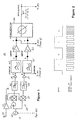
- a receiver and demodulator circuit 10 of Figure 1 comprises an antenna 20, RF amplifier 22, synchronous demodulator 30, filters 36, 37, 40, 41 and further amplifiers 38, 39, limiters 42, 43 and a four-phase detector 44.
- a transmitted FSK signal in which a data "1" state is represented by the carrier frequency modulated by, say, +f m and a data "0" state is represented by the carrier frequency modulated by -f m , is received by the antenna 20, amplified in the RF amplifier 22 and fed to the synchronous detector 30.
- the synchronous detector 30 comprises a local oscillator 32 and a 90° phase shifter 33 feeding, respectively, mixers 35 and 34.
- the RF signal from the amplifier 22 is fed to the other input of each of the mixers 34, 35 and the mixer outputs, which are in quadrature with each other, are taken to filters 36, 37, amplifiers 38, 39 and further filters 40, 41 before being amplitude-limited in limiters 42 and 43.
- the limited in-phase and quadrature signals are then processed in the four-phase detector 44, where the original transmitted data information is extracted and output along line 45.
- the filters 36, 37, 40 and 41 are all low-pass filters.
- the latter pair may, in practice, take the form of gyrators.
- An AFC circuit 50 (see Figure 3) is connected to a point B of Figure 1 and to the data output line 45.
- the baseband signal can be taken from any of points A-F, point B is chosen in this case in order to obtain a wide capture range, though this is at the expense of a narrow dynamic range, since point B is upstream of the limiting stages 42, 43.
- the baseband signal on line 51 (see Figure 3) is taken to the common pole C of a changeover switch 52, which in practice is a MOSFET analogue switch.
- the changeover poles 1, 2 of the switch 52 are connected to the inputs of frequency-to-voltage converters 54, 56, the outputs of each of which are taken to a sample-and-hold 58, 60.
- the sample-and-hold outputs feed a difference amplifier 64 which delivers, on line 66, an AFC signal for application to the oscillator 32 to be controlled.
- the data output from the FSK demodulator (line 45 of Figure 1) is taken along line 53 to the control input of the switch 52 and along line 55 to the control inputs of sample-and-holds 58, 60.
- An inverter 62 is included in the control line to one of the two sample-and-holds, so that they may be driven in anti-phase.
- the frequency of the local oscillator 32 will not remain absolutely constant, but will experience drift.
- the effect of such a drift can be seen in Figure 2, where the upper line shows the transmitted data, consisting of binary states, "1" and "0", and the lower line shows the baseband signal at any of points A-F. This baseband signal can be seen to vary in frequency, depending on the data state being transmitted.
- Converter 54 now converts the lower-than-normal baseband frequency into a corresponding voltage, which is sampled in sample-and-hold 58 and passed on to the difference amplifier 64. Meanwhile, the same change in state of the data signal has instructed the sample-and-hold 60 to hold the voltage corresponding to the higher-than-normal baseband frequency for the previous "0" data state, and this voltage is also passed on to difference amplifier 64. Difference amplifier 64 then subtracts the data "1" voltage from the data "0" voltage to form an output AFC voltage on line 66 which is fed back to the drifted oscillator 32 in such a sense as to reduce the difference between the data "1" and data "0" baseband frequencies.
- switch 52 changes over to pole 2, transferring the baseband signal on line 51 to converter 56, where its frequency is converted into a voltage which is sampled by sample-and-hold 56 and passed on to amplifier 64.
- sample-and-hold 58 is forced into its "hold” mode, so that the voltage output of converter 54 for the "1" state is held in sample-and-hold 58 and likewise fed to amplifier 64.
- Amplifier 64 forms the difference between the two voltages and sends this as a correcting signal back to the oscillator 32 as before.
- a second embodiment of the invention illustrated in Figure 4 in conjunction with Figure 1, employs digital techniques instead of analogue.
- the receiver and demodulator 10 is interfaced with a digital version 100 of the AFC circuit of the invention, the interfacing being arranged this time to allow for a wide dynamic range at the expense of capture range. This is achieved by taking the baseband signal from a point E of the receiver circuitry in Figure 1. Since this point is downstream of the limiter 42, the AFC circuit will work with an increased dynamic range over the arrangement shown in Figure 3.
- the baseband signal is taken on line 51 to the clocking inputs 75, 76 of two counters 80, 82, which correspond in this embodiment to the frequency-to-voltage converters of the previous embodiment.
- Each counter feeds a latch 84, 86, the output of which is taken to a digital subtractor 88.
- the data output signal from line 45 of Figure 1 is taken directly to gating input 83 of counter 82 and to latch-command input 85 of latch 84; similarly, an inverted version of the data output signal, by virtue of inverter 92, is taken to the gating input 81 of counter 80 and to the latch-command input 87 of latch 86.
- the output of the digital subtractor is taken to a D/A converter 90, the output of which is fed along line 94 back to the oscillator 32 whose frequency is to be corrected.
- the invention has been described in terms of the derivation of an AFC signal from a changing data output, the invention is not restricted to providing an AFC signal only when data is seen at the output. Thus, even when data is lost due to excessive drift, the arrangement according to the invention will still provide an AFC direction signal. This is primarily due to the fact that the output data signal will remain in either the high or low state when excessive frequency error occurs.
- the baseband pickup point may be at any of the points A-F, i.e. either before or after the filters 40, 41, or indeed, after the limiters 42, 43.
Landscapes
- Physics & Mathematics (AREA)
- Spectroscopy & Molecular Physics (AREA)
- Engineering & Computer Science (AREA)
- Computer Networks & Wireless Communication (AREA)
- Signal Processing (AREA)
- Digital Transmission Methods That Use Modulated Carrier Waves (AREA)
- Channel Selection Circuits, Automatic Tuning Circuits (AREA)
- Stabilization Of Oscillater, Synchronisation, Frequency Synthesizers (AREA)
- Superheterodyne Receivers (AREA)
Description
- The invention concerns an automatic frequency control arrangement, and in particular an automatic frequency control arrangement for use in a homodyne FSK (frequency shift keying) receiver or transceiver.
- Communication systems are known which operate by modulating a carrier according to the binary state of a data signal to be transmitted. In such systems, a binary "1" causes the carrier frequency to be shifted by a certain amount in one direction, while a binary "0" causes normally an equal shift in the opposite direction. For this reason, the technique is known as "frequency shift keying" (FSK) and when the shifts are the same in both directions, "symmetrical frequency shift keying".
- The local oscillator of a receiver in such an FSK system normally operates at the same frequency as the transmitter carrier, with the result that the signal at the output of the receiver mixer is at baseband IF frequency. This technique is known as "direct conversion" or "homodyne conversion". In an ideal system, where the local oscillator and transmitting oscillator frequencies are the same and the carrier is modulated symmetrically, i.e. is modulated plus and minus, respectively, by equal amounts for the two data states, the mixer output should always be at the same frequency, the baseband frequency, regardless of whether a "1" or a "0" is being received. There will, however, be a phase difference between the I and the Q channels due to the opposing signs of the modulating frequencies for the two data states, and it is this phase difference which is processed in the four-
phase detector 44 to reconstitute the transmitted data. - In a practical system, however, there may well be a difference between the carrier and local oscillator frequencies due to drifts in either or both of the oscillators. This drift may be due to various factors such as temperature variations, ageing, etc. When this occurs, the received IF frequency for a "1" state will be different from that for a "0" state and as a result the four-phase detector may be unable reliably to extract the transmitted data; indeed, when drift is excessive data may be totally lost.
- It is an aim of the invention to provide an automatic frequency control arrangement which overcomes the above drawback.
- GB-A-2137836 discloses an FM demodulator having automatic frequency control.
- According to a first aspect of the invention, there is provided an automatic frequency control arrangement, for use in a homodyne frequency shift keying (FSK) receiver, comprising: means for inputting a baseband signal from the receiver; and means for inputting a data signal from the receiver; characterised by means for forming first and second values representative of the frequency of the baseband signal for a first data state and for a second data state, respectively; means responsive to the data signal inputting means for forming the difference of the first and second values to provide a difference signal, and means for applying the difference signal to a local oscillator in the FSK homodyne receiver to control the frequency of the oscillator.
- The invention gives rise to a number of advantages when used in a symmetrical FSK homodyne receiver: principally, that all sources of drift, e.g. temperature, are compensated for by the closed loop of the automatic frequency control (AFC) circuit, and also that, when the AFC circuit operates at audio frequencies (typically 4.5kHz), it can be built very cheaply using non-critical components and layout.
- The circuit may be employed in either a single-quadrant or a multi-quadrant FSK receiver.
- The invention is useful not only for correcting for drift in the local oscillator of a receiver, but also for correcting for drift in a transmitting oscillator employed in a transceiver.
- The circuit may be realised in either analogue or digital form. In the analogue case, the baseband frequency for each of the first and second data states is converted into a corresponding value by a frequency-to-voltage converting means and this value is held, when the data signal changes state, in an associated sample-and-hold means, one per data state. The outputs of the two sample-and-hold means are taken to a difference-forming means and the output of the difference-forming means is used to correct the frequency of the oscillator.
- Either one frequency-to-voltage converting means may be used, fed directly from the baseband signal, the converting means being switched to one or other of the two sample-and-hold means in accordance with the data signal state, or two frequency-to-voltage converting means may be used, one per sample-and-hold means, the baseband signal being switched to one or other of the frequency-to-voltage converting means according to the data signal state.
- A digital realisation of the circuit according to the invention employs counting means and latching means instead of frequency-to-voltage converting means and sample-and-hold means to form and store a value representing the baseband frequency for each of the first and second data states. Instead of a difference amplifier, the difference-forming means is constituted by a digital subtracting means, which takes the difference between the contents of the two latches and passes it on to the control input of the local oscillator. Where the oscillator will accept a digital control input directly, as in a digitally controlled frequency synthesiser, for example, the output of the digital subtracting means may be used to effect control without further processing; where, however, the oscillator requires an analogue control input, it is necessary to interpose a digital-to-analogue converter between the digital subtracting means and the oscillator.
- As an alternative to analogue or digital realisation, the invention may be put into effect using software techniques.
- According to a second aspect of the invention, there is provided a homodyne FSK receiver or transceiver, characterised by comprising an automatic frequency control arrangement as described above.
- According to a third aspect of the invention, there is provided a method of controlling frequency in a homodyne FSK receiver or transceiver, characterised by the steps of: forming a value representative of the frequency of the baseband signal for a first data state; forming a value representative of the frequency of the baseband signal for a second data state; forming the difference of the two values to provide a difference signal, and applying the difference signal to a local oscillator in the receiver to control the frequency of the oscillator.
- The method may perform the steps of: converting the baseband frequency representative of a first data state to a corresponding first voltage signal, while storing a second voltage signal corresponding to the baseband frequency representative of a preceding second data state; converting the baseband frequency representative of a succeeding second data state to a corresponding second voltage signal, while storing the first voltage signal corresponding to the baseband frequency representative of the first data state; forming the difference of the two stored voltages, and applying the difference signal to the local oscillator in the receiver to control the frequency of the oscillator.
- The baseband frequency may be converted into first and second analogue voltage signals, or alternatively into first and second digital voltage signals.
- The invention will now be described, by way of example only, with reference to the drawings, of which:
- Figure 1 is a schematic diagram of an FSK receiver and demodulator circuit according to the invention;
- Figure 2 is a diagram showing the change in frequency of the baseband signal for a change in state of the data output signal in a non-ideal FSK receiver;
- Figure 3 is a schematic diagram of an automatic frequency control arrangement according to a first embodiment of the invention, and
- Figure 4 is a schematic diagram of an automatic frequency control arrangement according to a second embodiment of the invention.
-
- An AFC arrangement according to a first embodiment of the invention is shown in Figure 3 in conjunction with Figure 1. A receiver and
demodulator circuit 10 of Figure 1 comprises an antenna 20,RF amplifier 22,synchronous demodulator 30,filters further amplifiers limiters 42, 43 and a four-phase detector 44. A transmitted FSK signal, in which a data "1" state is represented by the carrier frequency modulated by, say, +fm and a data "0" state is represented by the carrier frequency modulated by -fm, is received by the antenna 20, amplified in theRF amplifier 22 and fed to thesynchronous detector 30. Thesynchronous detector 30 comprises a local oscillator 32 and a 90°phase shifter 33 feeding, respectively,mixers 35 and 34. The RF signal from theamplifier 22 is fed to the other input of each of themixers 34, 35 and the mixer outputs, which are in quadrature with each other, are taken tofilters 36, 37,amplifiers further filters 40, 41 before being amplitude-limited inlimiters 42 and 43. The limited in-phase and quadrature signals are then processed in the four-phase detector 44, where the original transmitted data information is extracted and output along line 45. - The
filters - An AFC circuit 50 (see Figure 3) is connected to a point B of Figure 1 and to the data output line 45. Although the baseband signal can be taken from any of points A-F, point B is chosen in this case in order to obtain a wide capture range, though this is at the expense of a narrow dynamic range, since point B is upstream of the
limiting stages 42, 43. The baseband signal on line 51 (see Figure 3) is taken to the common pole C of achangeover switch 52, which in practice is a MOSFET analogue switch. Thechangeover poles switch 52 are connected to the inputs of frequency-to-voltage converters 54, 56, the outputs of each of which are taken to a sample-and-hold 58, 60. The sample-and-hold outputs feed a difference amplifier 64 which delivers, online 66, an AFC signal for application to the oscillator 32 to be controlled. - The data output from the FSK demodulator (line 45 of Figure 1) is taken along line 53 to the control input of the
switch 52 and along line 55 to the control inputs of sample-and-holds 58, 60. Aninverter 62 is included in the control line to one of the two sample-and-holds, so that they may be driven in anti-phase. - In practice, the frequency of the local oscillator 32 will not remain absolutely constant, but will experience drift. The effect of such a drift can be seen in Figure 2, where the upper line shows the transmitted data, consisting of binary states, "1" and "0", and the lower line shows the baseband signal at any of points A-F. This baseband signal can be seen to vary in frequency, depending on the data state being transmitted. To give a concrete example, if it is assumed that the modulation frequency, fm, for each of the two data states is 4.5kHz and the local oscillator, for example, has drifted high by 1kHz, then the baseband frequency for, say, a "1" will be 4.5kHz - 1kHz = 3.5kHz, while that for a "0" will be 4.5kHz + 1kHz = 5.5kHz.
- The frequency-controlling operation of this first embodiment is as follows:
- Assume, firstly, that the local oscillator 32 in
demodulator 10 has drifted high, resulting in the baseband signal shown in Figure 2; secondly, that frequency-to-voltage converter 54 is allotted to the data "1" state, while frequency-to-voltage converter 56 is allotted to the data "0" state; thirdly, that thedemodulator 10 has started to register a data "1" state, having previously received a data "0" state. Upon the change of data state from "0" to "1", theanalogue switch 52 switches topole 1 and transfers the baseband signal fromline 51 to converter 54. Converter 54 now converts the lower-than-normal baseband frequency into a corresponding voltage, which is sampled in sample-and-hold 58 and passed on to the difference amplifier 64. Meanwhile, the same change in state of the data signal has instructed the sample-and-hold 60 to hold the voltage corresponding to the higher-than-normal baseband frequency for the previous "0" data state, and this voltage is also passed on to difference amplifier 64. Difference amplifier 64 then subtracts the data "1" voltage from the data "0" voltage to form an output AFC voltage online 66 which is fed back to the drifted oscillator 32 in such a sense as to reduce the difference between the data "1" and data "0" baseband frequencies. - In similar fashion, when the data output changes from a "1" to a "0" state, switch 52 changes over to
pole 2, transferring the baseband signal online 51 to converter 56, where its frequency is converted into a voltage which is sampled by sample-and-hold 56 and passed on to amplifier 64. At the same time, sample-and-hold 58 is forced into its "hold" mode, so that the voltage output of converter 54 for the "1" state is held in sample-and-hold 58 and likewise fed to amplifier 64. Amplifier 64 forms the difference between the two voltages and sends this as a correcting signal back to the oscillator 32 as before. - Clearly, it is possible, instead of employing two frequency-to-voltage converters, to use only one situated upstream of the
analogue switch 52.Poles switch 52 would then be taken directly to the inputs of the sample-and-holds 58, 60. While this would undoubtedly be more economical in hardware, there could well be a risk of charge-injection problems from the changeover of the data signal state, sinceswitch 52 would be handling not alternating signals, in which frequency, not DC level, was important, but DC signals from the frequency-to-voltage converter output. - A second embodiment of the invention, illustrated in Figure 4 in conjunction with Figure 1, employs digital techniques instead of analogue. In this embodiment, the receiver and
demodulator 10 is interfaced with adigital version 100 of the AFC circuit of the invention, the interfacing being arranged this time to allow for a wide dynamic range at the expense of capture range. This is achieved by taking the baseband signal from a point E of the receiver circuitry in Figure 1. Since this point is downstream of the limiter 42, the AFC circuit will work with an increased dynamic range over the arrangement shown in Figure 3. - In the
AFC arrangement 100 of Figure 4, the baseband signal is taken online 51 to the clockinginputs latch digital subtractor 88. The data output signal from line 45 of Figure 1 is taken directly to gatinginput 83 of counter 82 and to latch-command input 85 oflatch 84; similarly, an inverted version of the data output signal, by virtue ofinverter 92, is taken to thegating input 81 of counter 80 and to the latch-command input 87 oflatch 86. The output of the digital subtractor is taken to a D/A converter 90, the output of which is fed along line 94 back to the oscillator 32 whose frequency is to be corrected. - Looking at the mode of operation of this embodiment now, it is again assumed firstly that the local oscillator in
demodulator 10 has drifted high, resulting in the baseband signal shown in Figure 2; secondly, that counter 80 is allotted to the data "1" state, while counter 82 is allotted to the data "0" state; thirdly, that thedemodulator 10 has started to register a data "1" state, having previously received a data "0" state. At the changeover from data "0" to data "1", line 77 goes high and, assuming thegate inputs command inputs inverter 92 in the control line 78 to counter 80 andlatch 86, counter 80 starts to count at a rate corresponding to the baseband frequency for data state "1". At the same time, due to the low on line 78, latch 86 latches the count for the "0" state present in counter 82 at the transition from data "0" to data "1", while the high on line 77 inhibits the latching action oflatch 84. - The same action applies, but with both counters and latches reversed, at the transition from data "1" to data "0".
- Note that, in practice, the data string appearing on line 77 of Figure 4 would not consist exclusively of alternating "1"s and "0"s, but would occasionally consist of two or more consecutive similar states. In this situation, were the gating period of the counters 80 and 82 to correspond literally to the data "1" or data "0" time slots, unequal gating periods would result for the two counters, resulting in a false indication of baseband frequency for one or other of the two data states. To overcome this, counters 80, 82 are in practice equipped with some kind of monostable gating input, such that they respond to the signal at their
inputs - As with the analogue embodiment of Figure 3, it may be possible in this embodiment also to dispense with one of the counters by switching the output of a single counter between the
latches - While the invention has been described in terms of the derivation of an AFC signal from a changing data output, the invention is not restricted to providing an AFC signal only when data is seen at the output. Thus, even when data is lost due to excessive drift, the arrangement according to the invention will still provide an AFC direction signal. This is primarily due to the fact that the output data signal will remain in either the high or low state when excessive frequency error occurs.
- It is also stressed that, while the first and second embodiments of the invention have been described as picking up their baseband signals from points B and E, respectively, of Figure 1, the baseband pickup point may be at any of the points A-F, i.e. either before or after the
filters 40, 41, or indeed, after thelimiters 42, 43.
Claims (15)
- An automatic frequency control arrangement, for use in a homodyne frequency shift keying (FSK) receiver, comprising: means (51, 52) for inputting a baseband signal from the receiver; and means (53, 55; 77, 78, 92) for inputting a data signal from the receiver; characterised by means (54, 56; 80, 82) for forming first and second values representative of the frequency of the baseband signal for a first data state and for a second data state, respectively; means (58, 60, 64; 84, 86, 88) responsive to the data signal inputting means (53, 55; 77, 78, 92) for forming the difference of the first and second values to provide a difference signal, and means (66; 90) for applying the difference signal to a local oscillator (32) in the homodyne FSK receiver to control the frequency of the oscillator (32).
- An automatic frequency control arrangement as claimed in claim 1, characterised in that the means for forming first and second values representative of the frequency of the baseband signal for a first data state and for a second data state comprises first and second frequency-to-voltage converting means (54, 56), respectively, and the difference-forming means comprises first and second sample-and-hold means (58, 60) fed from the first and second frequency-to-voltage converting means (54, 56), respectively, and a difference amplifier (64) having a first input fed from an output of the first sample-and-hold means (58) and a second input fed from an output of the second sample-and-hold means (60).
- An automatic frequency control arrangement as claimed in claim 2, characterised in that the means for inputting a baseband signal from the receiver comprises a changeover switching means (52), the changeover switching means (52) having a common terminal (C), which serves to receive the baseband signal, and first and second changeover terminals (1, 2) connected to respective inputs of the first and second frequency-to-voltage converting means (54, 56).
- An automatic frequency control arrangement as claimed in claim 3, characterised in that the means for inputting a data signal (53, 55; 77, 78, 92) is arranged, when the data signal is in its first state, to control the changeover switching means (52) to provide the baseband signal to the first frequency-to-voltage converting means (54), to control the first sample-and-hold means (58) to sample the first value, and to control the second sample-and-hold means (60) to hold the second value.
- An automatic frequency control arrangement as claimed in claim 1, characterised in that the means for forming first and second values representative of the frequency of the baseband signal for a first data state and for a second data state comprises a frequency-to-voltage converting means, and the difference-forming means comprises a changeover switching means, first and second sample-and-hold means (58, 60) and a difference amplifier (64), wherein an input of the frequency-to-voltage converting means serves to receive the baseband signal, the changeover switching means has a common terminal (C), which is connected to an output of the frequency-to-voltage converting means, and first and second changeover terminals (1, 2), which are connected to respective signal inputs of the first and second sample-and-hold means (58, 60), and the difference amplifier (64) has a first input fed from an output of the first sample-and-hold means (58) and a second input fed from an output of the second sample-and-hold means (60).
- An automatic frequency control arrangement as claimed in claim 5, characterised in that the means for inputting a data signal (53, 55; 77,78; 92) is arranged, when the data signal is in its first state, to control the changeover switching means to connect the output of the frequency-to-voltage converting means to the input of the first sample-and-hold means (58), to control the first sample-and-hold means (58) to sample the first value, and to control the second sample-and-hold means (60) to hold the second value.
- An automatic frequency control arrangement as claimed in claim 1, characterised in that the means for forming first and second values representative of the frequency of the baseband signal for a first data state and for a second data state comprises first and second counting means (80, 82), respectively, and the difference-forming means comprises first and second latching means (84, 86) fed from the first and second counting means (80, 82), respectively, and a digital subtracting means (88) having a first input fed from an output of the first latching means (84) and a second input fed from an output of the second latching means (86).
- An automatic frequency control arrangement as claimed in claim 6, characterised in that the first and second counting means have respective clocking inputs (75, 76) which are arranged to receive the baseband signal, and the means for inputting a data signal is arranged when the data signal changes from its second to its first data state, to control the first counting means (80) to start counting, to control the second counting means to stop counting, and to control the second latching means (86) to latch in the contents of the second counting means (82), and, when the data signal changes from its first to its second data state, to control the second counting means (82) to start counting, to control the first counting means (80), to stop counting, and to control the first latching means (84) to latch in the contents of the first counting means (80).
- An automatic frequency control arrangement as claimed in claim 8, characterised in that control of the first and second counting means (80, 82) and of the first and second latching means (84, 86) is by way of first and second gating inputs and first and second latch-command inputs respectively provided in the counting means and the latching means.
- An automatic frequency control arrangement as claimed in claim 9, characterised in that the means for applying the difference signal to the local oscillator comprises a digital-to-analogue converter (90) fed from the output of the digital subtracting means (88).
- A homodyne FSK receiver or transceiver, characterised by comprising an automatic frequency control arrangement as claimed in any one of claims 1 to 10.
- A method of controlling frequency in a homodyne FSK receiver, characterised by the steps of: forming a value representative of the frequency of a baseband signal for a first data state; forming a value representative of the frequency of the baseband signal for a second data state; forming the difference of the two values to provide a difference signal, and applying the difference signal to a local oscillator in the receiver to control the frequency of the oscillator.
- A method of controlling frequency in a homodyne FSK receiver as claimed in claim 12, characterised by the steps of: converting the baseband frequency representative of a first data state to a corresponding first voltage signal, while storing a second voltage signal corresponding to the baseband frequency representative of a preceding second data state; converting the baseband frequency representative of a succeeding second data state to a corresponding second voltage signal, while storing the first voltage signal corresponding to the baseband frequency representative of the first data state; forming the difference of the two stored voltages and applying the difference signal to the local oscillator (32) in the receiver to control the frequency of the oscillator (32).
- A method of controlling frequency in a homodyne FSK receiver as claimed in claim 13, characterised in that the baseband frequency is converted into first and second analogue voltage signals.
- A method of controlling frequency in a homodyne FSK receiver as claimed in claim 13, characterised in that the baseband frequency is converted into first and second digital voltage signals.
Applications Claiming Priority (2)
| Application Number | Priority Date | Filing Date | Title |
|---|---|---|---|
| GB9316363A GB2280801B (en) | 1993-08-06 | 1993-08-06 | Automatic frequency control arrangement |
| GB9316363 | 1993-08-06 |
Publications (2)
| Publication Number | Publication Date |
|---|---|
| EP0637882A1 EP0637882A1 (en) | 1995-02-08 |
| EP0637882B1 true EP0637882B1 (en) | 2001-12-19 |
Family
ID=10740097
Family Applications (1)
| Application Number | Title | Priority Date | Filing Date |
|---|---|---|---|
| EP94304951A Expired - Lifetime EP0637882B1 (en) | 1993-08-06 | 1994-07-05 | Automatic frequency control arrangement |
Country Status (5)
| Country | Link |
|---|---|
| US (1) | US5530723A (en) |
| EP (1) | EP0637882B1 (en) |
| JP (1) | JP3493458B2 (en) |
| DE (1) | DE69429476T2 (en) |
| GB (1) | GB2280801B (en) |
Families Citing this family (10)
| Publication number | Priority date | Publication date | Assignee | Title |
|---|---|---|---|---|
| US5701600A (en) * | 1995-07-17 | 1997-12-23 | Motorola, Inc. | Radio receiver and method of calibrating same |
| US5717721A (en) * | 1995-08-21 | 1998-02-10 | General Research Of Electronics, Inc. | Demodulation correcting circuit for FSK receiver |
| JPH10163756A (en) * | 1996-11-28 | 1998-06-19 | Fujitsu Ltd | Automatic frequency control device |
| JP3070733B2 (en) * | 1997-12-12 | 2000-07-31 | 日本電気株式会社 | Automatic frequency control method and device |
| US6388248B1 (en) * | 2000-07-06 | 2002-05-14 | Eaton Corporation | Control voltage isolation system for electrical rotating apparatus utilizing fiber optics and associated method |
| KR100374944B1 (en) * | 2001-02-02 | 2003-03-06 | 주식회사 젤라인 | Synchronizer of frequency shift keying type receiver for power line communication |
| US7369849B2 (en) * | 2002-08-06 | 2008-05-06 | General Motors Corporation | Method and system for registering an in-vehicle cellular phone |
| US7680224B2 (en) * | 2004-08-27 | 2010-03-16 | Silicon Laboratories Inc. | Apparatus and method for automatic frequency correction for a receiver system |
| US7822397B2 (en) * | 2004-08-27 | 2010-10-26 | Silicon Laboratories Inc. | Method and apparatus for frequency hopping medium access control in a wireless network |
| US7672356B2 (en) | 2005-05-19 | 2010-03-02 | Itt Manufacturing Enterprises, Inc. | Method and apparatus for detection of a frequency coded sequence in the presence of sinusoidal interference |
Family Cites Families (7)
| Publication number | Priority date | Publication date | Assignee | Title |
|---|---|---|---|---|
| GB2109201B (en) * | 1981-10-26 | 1985-03-27 | Philips Electronic Associated | Direct modulation fm receiver |
| GB2137836B (en) * | 1983-04-06 | 1986-07-23 | Multitone Electronics Plc | Fm demodulators |
| US4647864A (en) * | 1986-04-21 | 1987-03-03 | General Electric Company | Variable-delay, sine-cosine non-coherent demodulator |
| GB2213663A (en) * | 1987-12-11 | 1989-08-16 | Philips Electronic Associated | Data demodulator carrier phase locking |
| DE4013384A1 (en) * | 1990-04-26 | 1991-10-31 | Philips Patentverwaltung | RECEIVER WITH AN ARRANGEMENT FOR FREQUENCY DEPOSIT ESTIMATION |
| JPH0813049B2 (en) * | 1990-06-20 | 1996-02-07 | 三菱電機株式会社 | Frequency error detector |
| US5208835A (en) * | 1990-09-24 | 1993-05-04 | In-Situ, Inc. | Automatic frequency control system and method for frequency-shift-key data transmission systems |
-
1993
- 1993-08-06 GB GB9316363A patent/GB2280801B/en not_active Expired - Fee Related
-
1994
- 1994-07-05 EP EP94304951A patent/EP0637882B1/en not_active Expired - Lifetime
- 1994-07-05 DE DE69429476T patent/DE69429476T2/en not_active Expired - Fee Related
- 1994-07-29 JP JP19623794A patent/JP3493458B2/en not_active Expired - Fee Related
- 1994-08-03 US US08/285,407 patent/US5530723A/en not_active Expired - Lifetime
Also Published As
| Publication number | Publication date |
|---|---|
| GB2280801A (en) | 1995-02-08 |
| GB2280801B (en) | 1997-12-10 |
| GB9316363D0 (en) | 1993-09-29 |
| JPH07170302A (en) | 1995-07-04 |
| EP0637882A1 (en) | 1995-02-08 |
| JP3493458B2 (en) | 2004-02-03 |
| DE69429476D1 (en) | 2002-01-31 |
| US5530723A (en) | 1996-06-25 |
| DE69429476T2 (en) | 2002-05-16 |
Similar Documents
| Publication | Publication Date | Title |
|---|---|---|
| US5584068A (en) | Direct conversion receiver | |
| WO1994016505B1 (en) | Psk demodulator | |
| CA1235754A (en) | Digital demodulator arrangement for quadrature signals | |
| US5648985A (en) | Universal radio architecture for low-tier personal communication system | |
| US5440268A (en) | AFC circuit for QPSK demodulator | |
| EP0141422B1 (en) | Frequency detector | |
| US3940695A (en) | Doppler correction of transmission frequencies | |
| US5530723A (en) | Automatic frequency control arrangement | |
| ES8402479A1 (en) | Demodulator arrangement for signals which are frequency-modulated on a carrier wave. | |
| EP0127941A1 (en) | Demodulator logic for frequency shift keyed signals | |
| EP0651520B1 (en) | Control arrangements for digital radio receivers | |
| EP0054323B1 (en) | Clock pulse phase shifter | |
| US5926750A (en) | Receiver | |
| JPS5831065B2 (en) | FSK demodulator | |
| US5307378A (en) | Digital radio communication apparatus | |
| EP0259867B1 (en) | Demodulator for psk-modulated signals | |
| US5193103A (en) | Digital phase locked loop circuit | |
| CA2242075A1 (en) | 4-level fsk demodulator | |
| CN1104820A (en) | Detectors | |
| US5586147A (en) | Demodulation method using quadrature modulation | |
| US4757272A (en) | Four phase PSK demodulator | |
| US3108158A (en) | Synchronous detection multiplex system | |
| EP0151394B1 (en) | Demodulator for ditital fm signals | |
| US5020079A (en) | Apparatus for generating a minimum-shift-keying signal | |
| EP0134600B1 (en) | Fm demodulation circuit |
Legal Events
| Date | Code | Title | Description |
|---|---|---|---|
| PUAI | Public reference made under article 153(3) epc to a published international application that has entered the european phase |
Free format text: ORIGINAL CODE: 0009012 |
|
| AK | Designated contracting states |
Kind code of ref document: A1 Designated state(s): DE FR |
|
| 17P | Request for examination filed |
Effective date: 19950804 |
|
| RAP1 | Party data changed (applicant data changed or rights of an application transferred) |
Owner name: MITEL SEMICONDUCTOR LIMITED |
|
| 17Q | First examination report despatched |
Effective date: 20000407 |
|
| GRAG | Despatch of communication of intention to grant |
Free format text: ORIGINAL CODE: EPIDOS AGRA |
|
| GRAG | Despatch of communication of intention to grant |
Free format text: ORIGINAL CODE: EPIDOS AGRA |
|
| GRAH | Despatch of communication of intention to grant a patent |
Free format text: ORIGINAL CODE: EPIDOS IGRA |
|
| GRAH | Despatch of communication of intention to grant a patent |
Free format text: ORIGINAL CODE: EPIDOS IGRA |
|
| GRAA | (expected) grant |
Free format text: ORIGINAL CODE: 0009210 |
|
| AK | Designated contracting states |
Kind code of ref document: B1 Designated state(s): DE FR |
|
| REF | Corresponds to: |
Ref document number: 69429476 Country of ref document: DE Date of ref document: 20020131 |
|
| PLBE | No opposition filed within time limit |
Free format text: ORIGINAL CODE: 0009261 |
|
| STAA | Information on the status of an ep patent application or granted ep patent |
Free format text: STATUS: NO OPPOSITION FILED WITHIN TIME LIMIT |
|
| 26N | No opposition filed | ||
| REG | Reference to a national code |
Ref country code: FR Ref legal event code: CD |
|
| PGFP | Annual fee paid to national office [announced via postgrant information from national office to epo] |
Ref country code: FR Payment date: 20030711 Year of fee payment: 10 |
|
| PGFP | Annual fee paid to national office [announced via postgrant information from national office to epo] |
Ref country code: DE Payment date: 20030717 Year of fee payment: 10 |
|
| PG25 | Lapsed in a contracting state [announced via postgrant information from national office to epo] |
Ref country code: DE Free format text: LAPSE BECAUSE OF NON-PAYMENT OF DUE FEES Effective date: 20050201 |
|
| PG25 | Lapsed in a contracting state [announced via postgrant information from national office to epo] |
Ref country code: FR Free format text: LAPSE BECAUSE OF NON-PAYMENT OF DUE FEES Effective date: 20050331 |
|
| REG | Reference to a national code |
Ref country code: FR Ref legal event code: ST |