EP0637862A2 - Semiconductor laser device and method of fabricating the laser device - Google Patents
Semiconductor laser device and method of fabricating the laser device Download PDFInfo
- Publication number
- EP0637862A2 EP0637862A2 EP94111892A EP94111892A EP0637862A2 EP 0637862 A2 EP0637862 A2 EP 0637862A2 EP 94111892 A EP94111892 A EP 94111892A EP 94111892 A EP94111892 A EP 94111892A EP 0637862 A2 EP0637862 A2 EP 0637862A2
- Authority
- EP
- European Patent Office
- Prior art keywords
- layer
- compound semiconductor
- laser device
- thickness
- compound
- Prior art date
- Legal status (The legal status is an assumption and is not a legal conclusion. Google has not performed a legal analysis and makes no representation as to the accuracy of the status listed.)
- Ceased
Links
Images


Classifications
-
- H—ELECTRICITY
- H01—ELECTRIC ELEMENTS
- H01S—DEVICES USING THE PROCESS OF LIGHT AMPLIFICATION BY STIMULATED EMISSION OF RADIATION [LASER] TO AMPLIFY OR GENERATE LIGHT; DEVICES USING STIMULATED EMISSION OF ELECTROMAGNETIC RADIATION IN WAVE RANGES OTHER THAN OPTICAL
- H01S5/00—Semiconductor lasers
- H01S5/30—Structure or shape of the active region; Materials used for the active region
- H01S5/32—Structure or shape of the active region; Materials used for the active region comprising PN junctions, e.g. hetero- or double- heterostructures
- H01S5/327—Structure or shape of the active region; Materials used for the active region comprising PN junctions, e.g. hetero- or double- heterostructures in AIIBVI compounds, e.g. ZnCdSe-laser
-
- H—ELECTRICITY
- H01—ELECTRIC ELEMENTS
- H01L—SEMICONDUCTOR DEVICES NOT COVERED BY CLASS H10
- H01L33/00—Semiconductor devices with at least one potential-jump barrier or surface barrier specially adapted for light emission; Processes or apparatus specially adapted for the manufacture or treatment thereof or of parts thereof; Details thereof
- H01L33/36—Semiconductor devices with at least one potential-jump barrier or surface barrier specially adapted for light emission; Processes or apparatus specially adapted for the manufacture or treatment thereof or of parts thereof; Details thereof characterised by the electrodes
- H01L33/40—Materials therefor
-
- B—PERFORMING OPERATIONS; TRANSPORTING
- B82—NANOTECHNOLOGY
- B82Y—SPECIFIC USES OR APPLICATIONS OF NANOSTRUCTURES; MEASUREMENT OR ANALYSIS OF NANOSTRUCTURES; MANUFACTURE OR TREATMENT OF NANOSTRUCTURES
- B82Y20/00—Nanooptics, e.g. quantum optics or photonic crystals
-
- H—ELECTRICITY
- H01—ELECTRIC ELEMENTS
- H01L—SEMICONDUCTOR DEVICES NOT COVERED BY CLASS H10
- H01L21/00—Processes or apparatus adapted for the manufacture or treatment of semiconductor or solid state devices or of parts thereof
- H01L21/02—Manufacture or treatment of semiconductor devices or of parts thereof
- H01L21/02104—Forming layers
- H01L21/02365—Forming inorganic semiconducting materials on a substrate
- H01L21/02367—Substrates
- H01L21/0237—Materials
- H01L21/02387—Group 13/15 materials
- H01L21/02395—Arsenides
-
- H—ELECTRICITY
- H01—ELECTRIC ELEMENTS
- H01L—SEMICONDUCTOR DEVICES NOT COVERED BY CLASS H10
- H01L21/00—Processes or apparatus adapted for the manufacture or treatment of semiconductor or solid state devices or of parts thereof
- H01L21/02—Manufacture or treatment of semiconductor devices or of parts thereof
- H01L21/02104—Forming layers
- H01L21/02365—Forming inorganic semiconducting materials on a substrate
- H01L21/02436—Intermediate layers between substrates and deposited layers
- H01L21/02439—Materials
- H01L21/02455—Group 13/15 materials
- H01L21/02463—Arsenides
-
- H—ELECTRICITY
- H01—ELECTRIC ELEMENTS
- H01L—SEMICONDUCTOR DEVICES NOT COVERED BY CLASS H10
- H01L21/00—Processes or apparatus adapted for the manufacture or treatment of semiconductor or solid state devices or of parts thereof
- H01L21/02—Manufacture or treatment of semiconductor devices or of parts thereof
- H01L21/02104—Forming layers
- H01L21/02365—Forming inorganic semiconducting materials on a substrate
- H01L21/02436—Intermediate layers between substrates and deposited layers
- H01L21/02439—Materials
- H01L21/02469—Group 12/16 materials
- H01L21/02474—Sulfides
-
- H—ELECTRICITY
- H01—ELECTRIC ELEMENTS
- H01L—SEMICONDUCTOR DEVICES NOT COVERED BY CLASS H10
- H01L21/00—Processes or apparatus adapted for the manufacture or treatment of semiconductor or solid state devices or of parts thereof
- H01L21/02—Manufacture or treatment of semiconductor devices or of parts thereof
- H01L21/02104—Forming layers
- H01L21/02365—Forming inorganic semiconducting materials on a substrate
- H01L21/02436—Intermediate layers between substrates and deposited layers
- H01L21/02439—Materials
- H01L21/02469—Group 12/16 materials
- H01L21/02477—Selenides
-
- H—ELECTRICITY
- H01—ELECTRIC ELEMENTS
- H01L—SEMICONDUCTOR DEVICES NOT COVERED BY CLASS H10
- H01L21/00—Processes or apparatus adapted for the manufacture or treatment of semiconductor or solid state devices or of parts thereof
- H01L21/02—Manufacture or treatment of semiconductor devices or of parts thereof
- H01L21/02104—Forming layers
- H01L21/02365—Forming inorganic semiconducting materials on a substrate
- H01L21/02436—Intermediate layers between substrates and deposited layers
- H01L21/02494—Structure
- H01L21/02496—Layer structure
- H01L21/02505—Layer structure consisting of more than two layers
- H01L21/02507—Alternating layers, e.g. superlattice
-
- H—ELECTRICITY
- H01—ELECTRIC ELEMENTS
- H01L—SEMICONDUCTOR DEVICES NOT COVERED BY CLASS H10
- H01L21/00—Processes or apparatus adapted for the manufacture or treatment of semiconductor or solid state devices or of parts thereof
- H01L21/02—Manufacture or treatment of semiconductor devices or of parts thereof
- H01L21/02104—Forming layers
- H01L21/02365—Forming inorganic semiconducting materials on a substrate
- H01L21/02518—Deposited layers
- H01L21/02521—Materials
- H01L21/02551—Group 12/16 materials
- H01L21/02557—Sulfides
-
- H—ELECTRICITY
- H01—ELECTRIC ELEMENTS
- H01L—SEMICONDUCTOR DEVICES NOT COVERED BY CLASS H10
- H01L21/00—Processes or apparatus adapted for the manufacture or treatment of semiconductor or solid state devices or of parts thereof
- H01L21/02—Manufacture or treatment of semiconductor devices or of parts thereof
- H01L21/02104—Forming layers
- H01L21/02365—Forming inorganic semiconducting materials on a substrate
- H01L21/02518—Deposited layers
- H01L21/02521—Materials
- H01L21/02551—Group 12/16 materials
- H01L21/0256—Selenides
-
- H—ELECTRICITY
- H01—ELECTRIC ELEMENTS
- H01L—SEMICONDUCTOR DEVICES NOT COVERED BY CLASS H10
- H01L21/00—Processes or apparatus adapted for the manufacture or treatment of semiconductor or solid state devices or of parts thereof
- H01L21/02—Manufacture or treatment of semiconductor devices or of parts thereof
- H01L21/02104—Forming layers
- H01L21/02365—Forming inorganic semiconducting materials on a substrate
- H01L21/02518—Deposited layers
- H01L21/0257—Doping during depositing
- H01L21/02573—Conductivity type
- H01L21/02576—N-type
-
- H—ELECTRICITY
- H01—ELECTRIC ELEMENTS
- H01L—SEMICONDUCTOR DEVICES NOT COVERED BY CLASS H10
- H01L21/00—Processes or apparatus adapted for the manufacture or treatment of semiconductor or solid state devices or of parts thereof
- H01L21/02—Manufacture or treatment of semiconductor devices or of parts thereof
- H01L21/02104—Forming layers
- H01L21/02365—Forming inorganic semiconducting materials on a substrate
- H01L21/02518—Deposited layers
- H01L21/0257—Doping during depositing
- H01L21/02573—Conductivity type
- H01L21/02579—P-type
-
- H—ELECTRICITY
- H01—ELECTRIC ELEMENTS
- H01L—SEMICONDUCTOR DEVICES NOT COVERED BY CLASS H10
- H01L33/00—Semiconductor devices with at least one potential-jump barrier or surface barrier specially adapted for light emission; Processes or apparatus specially adapted for the manufacture or treatment thereof or of parts thereof; Details thereof
- H01L33/005—Processes
- H01L33/0083—Processes for devices with an active region comprising only II-VI compounds
- H01L33/0087—Processes for devices with an active region comprising only II-VI compounds with a substrate not being a II-VI compound
-
- H—ELECTRICITY
- H01—ELECTRIC ELEMENTS
- H01L—SEMICONDUCTOR DEVICES NOT COVERED BY CLASS H10
- H01L33/00—Semiconductor devices with at least one potential-jump barrier or surface barrier specially adapted for light emission; Processes or apparatus specially adapted for the manufacture or treatment thereof or of parts thereof; Details thereof
- H01L33/02—Semiconductor devices with at least one potential-jump barrier or surface barrier specially adapted for light emission; Processes or apparatus specially adapted for the manufacture or treatment thereof or of parts thereof; Details thereof characterised by the semiconductor bodies
- H01L33/26—Materials of the light emitting region
- H01L33/28—Materials of the light emitting region containing only elements of group II and group VI of the periodic system
-
- H—ELECTRICITY
- H01—ELECTRIC ELEMENTS
- H01S—DEVICES USING THE PROCESS OF LIGHT AMPLIFICATION BY STIMULATED EMISSION OF RADIATION [LASER] TO AMPLIFY OR GENERATE LIGHT; DEVICES USING STIMULATED EMISSION OF ELECTROMAGNETIC RADIATION IN WAVE RANGES OTHER THAN OPTICAL
- H01S5/00—Semiconductor lasers
- H01S5/20—Structure or shape of the semiconductor body to guide the optical wave ; Confining structures perpendicular to the optical axis, e.g. index or gain guiding, stripe geometry, broad area lasers, gain tailoring, transverse or lateral reflectors, special cladding structures, MQW barrier reflection layers
- H01S5/22—Structure or shape of the semiconductor body to guide the optical wave ; Confining structures perpendicular to the optical axis, e.g. index or gain guiding, stripe geometry, broad area lasers, gain tailoring, transverse or lateral reflectors, special cladding structures, MQW barrier reflection layers having a ridge or stripe structure
- H01S5/227—Buried mesa structure ; Striped active layer
-
- H—ELECTRICITY
- H01—ELECTRIC ELEMENTS
- H01S—DEVICES USING THE PROCESS OF LIGHT AMPLIFICATION BY STIMULATED EMISSION OF RADIATION [LASER] TO AMPLIFY OR GENERATE LIGHT; DEVICES USING STIMULATED EMISSION OF ELECTROMAGNETIC RADIATION IN WAVE RANGES OTHER THAN OPTICAL
- H01S5/00—Semiconductor lasers
- H01S5/02—Structural details or components not essential to laser action
- H01S5/028—Coatings ; Treatment of the laser facets, e.g. etching, passivation layers or reflecting layers
- H01S5/0281—Coatings made of semiconductor materials
-
- H—ELECTRICITY
- H01—ELECTRIC ELEMENTS
- H01S—DEVICES USING THE PROCESS OF LIGHT AMPLIFICATION BY STIMULATED EMISSION OF RADIATION [LASER] TO AMPLIFY OR GENERATE LIGHT; DEVICES USING STIMULATED EMISSION OF ELECTROMAGNETIC RADIATION IN WAVE RANGES OTHER THAN OPTICAL
- H01S5/00—Semiconductor lasers
- H01S5/02—Structural details or components not essential to laser action
- H01S5/028—Coatings ; Treatment of the laser facets, e.g. etching, passivation layers or reflecting layers
- H01S5/0282—Passivation layers or treatments
-
- H—ELECTRICITY
- H01—ELECTRIC ELEMENTS
- H01S—DEVICES USING THE PROCESS OF LIGHT AMPLIFICATION BY STIMULATED EMISSION OF RADIATION [LASER] TO AMPLIFY OR GENERATE LIGHT; DEVICES USING STIMULATED EMISSION OF ELECTROMAGNETIC RADIATION IN WAVE RANGES OTHER THAN OPTICAL
- H01S5/00—Semiconductor lasers
- H01S5/04—Processes or apparatus for excitation, e.g. pumping, e.g. by electron beams
- H01S5/042—Electrical excitation ; Circuits therefor
- H01S5/0421—Electrical excitation ; Circuits therefor characterised by the semiconducting contacting layers
-
- H—ELECTRICITY
- H01—ELECTRIC ELEMENTS
- H01S—DEVICES USING THE PROCESS OF LIGHT AMPLIFICATION BY STIMULATED EMISSION OF RADIATION [LASER] TO AMPLIFY OR GENERATE LIGHT; DEVICES USING STIMULATED EMISSION OF ELECTROMAGNETIC RADIATION IN WAVE RANGES OTHER THAN OPTICAL
- H01S5/00—Semiconductor lasers
- H01S5/20—Structure or shape of the semiconductor body to guide the optical wave ; Confining structures perpendicular to the optical axis, e.g. index or gain guiding, stripe geometry, broad area lasers, gain tailoring, transverse or lateral reflectors, special cladding structures, MQW barrier reflection layers
- H01S5/2004—Confining in the direction perpendicular to the layer structure
- H01S5/2009—Confining in the direction perpendicular to the layer structure by using electron barrier layers
-
- H—ELECTRICITY
- H01—ELECTRIC ELEMENTS
- H01S—DEVICES USING THE PROCESS OF LIGHT AMPLIFICATION BY STIMULATED EMISSION OF RADIATION [LASER] TO AMPLIFY OR GENERATE LIGHT; DEVICES USING STIMULATED EMISSION OF ELECTROMAGNETIC RADIATION IN WAVE RANGES OTHER THAN OPTICAL
- H01S5/00—Semiconductor lasers
- H01S5/20—Structure or shape of the semiconductor body to guide the optical wave ; Confining structures perpendicular to the optical axis, e.g. index or gain guiding, stripe geometry, broad area lasers, gain tailoring, transverse or lateral reflectors, special cladding structures, MQW barrier reflection layers
- H01S5/22—Structure or shape of the semiconductor body to guide the optical wave ; Confining structures perpendicular to the optical axis, e.g. index or gain guiding, stripe geometry, broad area lasers, gain tailoring, transverse or lateral reflectors, special cladding structures, MQW barrier reflection layers having a ridge or stripe structure
- H01S5/2205—Structure or shape of the semiconductor body to guide the optical wave ; Confining structures perpendicular to the optical axis, e.g. index or gain guiding, stripe geometry, broad area lasers, gain tailoring, transverse or lateral reflectors, special cladding structures, MQW barrier reflection layers having a ridge or stripe structure comprising special burying or current confinement layers
- H01S5/2211—Structure or shape of the semiconductor body to guide the optical wave ; Confining structures perpendicular to the optical axis, e.g. index or gain guiding, stripe geometry, broad area lasers, gain tailoring, transverse or lateral reflectors, special cladding structures, MQW barrier reflection layers having a ridge or stripe structure comprising special burying or current confinement layers based on II-VI materials
-
- H—ELECTRICITY
- H01—ELECTRIC ELEMENTS
- H01S—DEVICES USING THE PROCESS OF LIGHT AMPLIFICATION BY STIMULATED EMISSION OF RADIATION [LASER] TO AMPLIFY OR GENERATE LIGHT; DEVICES USING STIMULATED EMISSION OF ELECTROMAGNETIC RADIATION IN WAVE RANGES OTHER THAN OPTICAL
- H01S5/00—Semiconductor lasers
- H01S5/20—Structure or shape of the semiconductor body to guide the optical wave ; Confining structures perpendicular to the optical axis, e.g. index or gain guiding, stripe geometry, broad area lasers, gain tailoring, transverse or lateral reflectors, special cladding structures, MQW barrier reflection layers
- H01S5/22—Structure or shape of the semiconductor body to guide the optical wave ; Confining structures perpendicular to the optical axis, e.g. index or gain guiding, stripe geometry, broad area lasers, gain tailoring, transverse or lateral reflectors, special cladding structures, MQW barrier reflection layers having a ridge or stripe structure
- H01S5/223—Buried stripe structure
- H01S5/2231—Buried stripe structure with inner confining structure only between the active layer and the upper electrode
-
- H—ELECTRICITY
- H01—ELECTRIC ELEMENTS
- H01S—DEVICES USING THE PROCESS OF LIGHT AMPLIFICATION BY STIMULATED EMISSION OF RADIATION [LASER] TO AMPLIFY OR GENERATE LIGHT; DEVICES USING STIMULATED EMISSION OF ELECTROMAGNETIC RADIATION IN WAVE RANGES OTHER THAN OPTICAL
- H01S5/00—Semiconductor lasers
- H01S5/20—Structure or shape of the semiconductor body to guide the optical wave ; Confining structures perpendicular to the optical axis, e.g. index or gain guiding, stripe geometry, broad area lasers, gain tailoring, transverse or lateral reflectors, special cladding structures, MQW barrier reflection layers
- H01S5/22—Structure or shape of the semiconductor body to guide the optical wave ; Confining structures perpendicular to the optical axis, e.g. index or gain guiding, stripe geometry, broad area lasers, gain tailoring, transverse or lateral reflectors, special cladding structures, MQW barrier reflection layers having a ridge or stripe structure
- H01S5/227—Buried mesa structure ; Striped active layer
- H01S5/2275—Buried mesa structure ; Striped active layer mesa created by etching
-
- H—ELECTRICITY
- H01—ELECTRIC ELEMENTS
- H01S—DEVICES USING THE PROCESS OF LIGHT AMPLIFICATION BY STIMULATED EMISSION OF RADIATION [LASER] TO AMPLIFY OR GENERATE LIGHT; DEVICES USING STIMULATED EMISSION OF ELECTROMAGNETIC RADIATION IN WAVE RANGES OTHER THAN OPTICAL
- H01S5/00—Semiconductor lasers
- H01S5/30—Structure or shape of the active region; Materials used for the active region
- H01S5/32—Structure or shape of the active region; Materials used for the active region comprising PN junctions, e.g. hetero- or double- heterostructures
- H01S5/3201—Structure or shape of the active region; Materials used for the active region comprising PN junctions, e.g. hetero- or double- heterostructures incorporating bulkstrain effects, e.g. strain compensation, strain related to polarisation
-
- H—ELECTRICITY
- H01—ELECTRIC ELEMENTS
- H01S—DEVICES USING THE PROCESS OF LIGHT AMPLIFICATION BY STIMULATED EMISSION OF RADIATION [LASER] TO AMPLIFY OR GENERATE LIGHT; DEVICES USING STIMULATED EMISSION OF ELECTROMAGNETIC RADIATION IN WAVE RANGES OTHER THAN OPTICAL
- H01S5/00—Semiconductor lasers
- H01S5/30—Structure or shape of the active region; Materials used for the active region
- H01S5/32—Structure or shape of the active region; Materials used for the active region comprising PN junctions, e.g. hetero- or double- heterostructures
- H01S5/3211—Structure or shape of the active region; Materials used for the active region comprising PN junctions, e.g. hetero- or double- heterostructures characterised by special cladding layers, e.g. details on band-discontinuities
- H01S5/3213—Structure or shape of the active region; Materials used for the active region comprising PN junctions, e.g. hetero- or double- heterostructures characterised by special cladding layers, e.g. details on band-discontinuities asymmetric clading layers
-
- H—ELECTRICITY
- H01—ELECTRIC ELEMENTS
- H01S—DEVICES USING THE PROCESS OF LIGHT AMPLIFICATION BY STIMULATED EMISSION OF RADIATION [LASER] TO AMPLIFY OR GENERATE LIGHT; DEVICES USING STIMULATED EMISSION OF ELECTROMAGNETIC RADIATION IN WAVE RANGES OTHER THAN OPTICAL
- H01S5/00—Semiconductor lasers
- H01S5/30—Structure or shape of the active region; Materials used for the active region
- H01S5/32—Structure or shape of the active region; Materials used for the active region comprising PN junctions, e.g. hetero- or double- heterostructures
- H01S5/3211—Structure or shape of the active region; Materials used for the active region comprising PN junctions, e.g. hetero- or double- heterostructures characterised by special cladding layers, e.g. details on band-discontinuities
- H01S5/3215—Structure or shape of the active region; Materials used for the active region comprising PN junctions, e.g. hetero- or double- heterostructures characterised by special cladding layers, e.g. details on band-discontinuities graded composition cladding layers
-
- H—ELECTRICITY
- H01—ELECTRIC ELEMENTS
- H01S—DEVICES USING THE PROCESS OF LIGHT AMPLIFICATION BY STIMULATED EMISSION OF RADIATION [LASER] TO AMPLIFY OR GENERATE LIGHT; DEVICES USING STIMULATED EMISSION OF ELECTROMAGNETIC RADIATION IN WAVE RANGES OTHER THAN OPTICAL
- H01S5/00—Semiconductor lasers
- H01S5/30—Structure or shape of the active region; Materials used for the active region
- H01S5/32—Structure or shape of the active region; Materials used for the active region comprising PN junctions, e.g. hetero- or double- heterostructures
- H01S5/3211—Structure or shape of the active region; Materials used for the active region comprising PN junctions, e.g. hetero- or double- heterostructures characterised by special cladding layers, e.g. details on band-discontinuities
- H01S5/3216—Structure or shape of the active region; Materials used for the active region comprising PN junctions, e.g. hetero- or double- heterostructures characterised by special cladding layers, e.g. details on band-discontinuities quantum well or superlattice cladding layers
-
- H—ELECTRICITY
- H01—ELECTRIC ELEMENTS
- H01S—DEVICES USING THE PROCESS OF LIGHT AMPLIFICATION BY STIMULATED EMISSION OF RADIATION [LASER] TO AMPLIFY OR GENERATE LIGHT; DEVICES USING STIMULATED EMISSION OF ELECTROMAGNETIC RADIATION IN WAVE RANGES OTHER THAN OPTICAL
- H01S5/00—Semiconductor lasers
- H01S5/30—Structure or shape of the active region; Materials used for the active region
- H01S5/32—Structure or shape of the active region; Materials used for the active region comprising PN junctions, e.g. hetero- or double- heterostructures
- H01S5/3211—Structure or shape of the active region; Materials used for the active region comprising PN junctions, e.g. hetero- or double- heterostructures characterised by special cladding layers, e.g. details on band-discontinuities
- H01S5/3218—Structure or shape of the active region; Materials used for the active region comprising PN junctions, e.g. hetero- or double- heterostructures characterised by special cladding layers, e.g. details on band-discontinuities specially strained cladding layers, other than for strain compensation
-
- H—ELECTRICITY
- H01—ELECTRIC ELEMENTS
- H01S—DEVICES USING THE PROCESS OF LIGHT AMPLIFICATION BY STIMULATED EMISSION OF RADIATION [LASER] TO AMPLIFY OR GENERATE LIGHT; DEVICES USING STIMULATED EMISSION OF ELECTROMAGNETIC RADIATION IN WAVE RANGES OTHER THAN OPTICAL
- H01S5/00—Semiconductor lasers
- H01S5/30—Structure or shape of the active region; Materials used for the active region
- H01S5/34—Structure or shape of the active region; Materials used for the active region comprising quantum well or superlattice structures, e.g. single quantum well [SQW] lasers, multiple quantum well [MQW] lasers or graded index separate confinement heterostructure [GRINSCH] lasers
- H01S5/3403—Structure or shape of the active region; Materials used for the active region comprising quantum well or superlattice structures, e.g. single quantum well [SQW] lasers, multiple quantum well [MQW] lasers or graded index separate confinement heterostructure [GRINSCH] lasers having a strained layer structure in which the strain performs a special function, e.g. general strain effects, strain versus polarisation
- H01S5/3406—Structure or shape of the active region; Materials used for the active region comprising quantum well or superlattice structures, e.g. single quantum well [SQW] lasers, multiple quantum well [MQW] lasers or graded index separate confinement heterostructure [GRINSCH] lasers having a strained layer structure in which the strain performs a special function, e.g. general strain effects, strain versus polarisation including strain compensation
-
- H—ELECTRICITY
- H01—ELECTRIC ELEMENTS
- H01S—DEVICES USING THE PROCESS OF LIGHT AMPLIFICATION BY STIMULATED EMISSION OF RADIATION [LASER] TO AMPLIFY OR GENERATE LIGHT; DEVICES USING STIMULATED EMISSION OF ELECTROMAGNETIC RADIATION IN WAVE RANGES OTHER THAN OPTICAL
- H01S5/00—Semiconductor lasers
- H01S5/30—Structure or shape of the active region; Materials used for the active region
- H01S5/34—Structure or shape of the active region; Materials used for the active region comprising quantum well or superlattice structures, e.g. single quantum well [SQW] lasers, multiple quantum well [MQW] lasers or graded index separate confinement heterostructure [GRINSCH] lasers
- H01S5/3409—Structure or shape of the active region; Materials used for the active region comprising quantum well or superlattice structures, e.g. single quantum well [SQW] lasers, multiple quantum well [MQW] lasers or graded index separate confinement heterostructure [GRINSCH] lasers special GRINSCH structures
-
- H—ELECTRICITY
- H01—ELECTRIC ELEMENTS
- H01S—DEVICES USING THE PROCESS OF LIGHT AMPLIFICATION BY STIMULATED EMISSION OF RADIATION [LASER] TO AMPLIFY OR GENERATE LIGHT; DEVICES USING STIMULATED EMISSION OF ELECTROMAGNETIC RADIATION IN WAVE RANGES OTHER THAN OPTICAL
- H01S5/00—Semiconductor lasers
- H01S5/30—Structure or shape of the active region; Materials used for the active region
- H01S5/34—Structure or shape of the active region; Materials used for the active region comprising quantum well or superlattice structures, e.g. single quantum well [SQW] lasers, multiple quantum well [MQW] lasers or graded index separate confinement heterostructure [GRINSCH] lasers
- H01S5/3422—Structure or shape of the active region; Materials used for the active region comprising quantum well or superlattice structures, e.g. single quantum well [SQW] lasers, multiple quantum well [MQW] lasers or graded index separate confinement heterostructure [GRINSCH] lasers comprising type-II quantum wells or superlattices
-
- H—ELECTRICITY
- H01—ELECTRIC ELEMENTS
- H01S—DEVICES USING THE PROCESS OF LIGHT AMPLIFICATION BY STIMULATED EMISSION OF RADIATION [LASER] TO AMPLIFY OR GENERATE LIGHT; DEVICES USING STIMULATED EMISSION OF ELECTROMAGNETIC RADIATION IN WAVE RANGES OTHER THAN OPTICAL
- H01S5/00—Semiconductor lasers
- H01S5/30—Structure or shape of the active region; Materials used for the active region
- H01S5/34—Structure or shape of the active region; Materials used for the active region comprising quantum well or superlattice structures, e.g. single quantum well [SQW] lasers, multiple quantum well [MQW] lasers or graded index separate confinement heterostructure [GRINSCH] lasers
- H01S5/347—Structure or shape of the active region; Materials used for the active region comprising quantum well or superlattice structures, e.g. single quantum well [SQW] lasers, multiple quantum well [MQW] lasers or graded index separate confinement heterostructure [GRINSCH] lasers in AIIBVI compounds, e.g. ZnCdSe- laser
Definitions
- the present invention relates to a semiconductor laser device, and particularly to a short wave semiconductor laser device composed of a II-VI compound semiconductor used for information processing terminal equipment such as an optical disk, laser beam printer or laser television, and a method of fabricating the laser device.
- a conventional semiconductor laser device using a II-VI compound semiconductor has a gain waveguiding type electrode stripe structure in which an alloy of ZnCdSSe or ZnMgSSe is grown on a GaAs substrate.
- the former structure using ZnCdSSe has been described, for example in Unexamined Japanese Patent Publication No. HEI 3-91270; and the latter structure using ZnMgSSe has been described, for example in Unexamined Japanese Patent Publication No. HEI 5-75217.
- a continuous oscillation at low temperatures or a pulse oscillation at room temperature can be realized at an oscillation wavelength of about 500 nm (ZnCdSSe system) or about 450 nm (ZnMgSSe system).
- the threshold current is relatively large because of the gain waveguiding type. It is difficult to form an ohmic contact with an electrode material because of the wide gap material. The thermal expansion strain remains in the device because a III-V compound semiconductor is used as a growth substrate. It is difficult to design a laser structure with a large band continuity between a clad layer and an active layer for the ZnCdSSe system being easy in the conducting control compared with the ZnMgSSe system, resulting in the insufficient confinement of injected charge and light. Because of these disadvantages, the above structures are difficult to achieve the continuous oscillation at room temperature and the operation with a high reliability.
- An object of the present invention is to provide a short wave semiconductor laser device composed of a II-VI compound semiconductor capable of solving the above-described problems.
- the present invention basically includes a buried type semiconductor laser structure using a II-VI compound semiconductor for reducing the threshold current and improving the reliability, wherein a multi-layer reflection film is provided for achieving the short wave oscillation.
- a buried type semiconductor laser device composed of a II-VI compound semiconductor a buried layer is made of a II-VI compound semiconductor having a refraction factor lower than that of an active layer of the laser device.
- the buried layer has a forbidden band width larger than that of an active layer of the laser device.
- the buried layer has such a composition that the lattice constant thereof is substantially matched to that of a substrate on which the laser device is grown, and also it has an electric resistance high enough not to exert an effect on the operation of the laser composed of an n-type clad-active layer-a p-type clad.
- the buried layer is made of a II-VI compound semiconductor having a conducting type opposed to that of a clad layer being horizontally contacted with the surface of a substrate or to that of an active layer.
- the method of forming a buried layer includes the steps of: forming sulfur atoms or a layer of sulfur atoms on a II-VI compound semiconductor; introducing the II-VI compound semiconductor in a thin film deposition apparatus; removing the sulfur atoms or a layer of sulfur atoms by a suitable amount using electromagnetic wave, corpuscular beam, heat or solution; and growing or depositing a new material of a II-VI compound semiconductor, a III-V compound, a IV compound, a IV-VI compound, or a II-VII compound.
- the sulfur atoms or a layer of sulfur atoms formed on the II-VI compound semiconductor are removed at a temperature of 400°C or less, and a new material of a II-VI compound semiconductor, a III-V compound, a IV compound, a IV-VI compound, or a II-VII compound is grown or deposited on the exposed surface.
- a material, which is used for formation of a protection film or multi-layer reflection film at the end surface of a resonator, contains one kind or more of II-VI compounds having a forbidden band width larger than that of an active layer, such as ZnS or MgS; one kind or more of IV-VI compounds having a forbidden band width larger than that of an active layer, such as SiO2 or TiO2; one kind or more of II-VII compounds having a forbidden band width larger than that of an active layer, such as MgF2 or CaF2; or one kind or more of IV compounds having a forbidden band width larger than that of an active layer, such as C, SiCx or SiNx.
- a cap layer is made of a P-type CdSSe alloy having a small energy difference on the valency electron side to the clad layer and a relatively narrow forbidden band width.
- the cap layer made of an alloy with a gradient composition can be easily fabricated by exposing the surface of a clad layer to a molecular beam of Cd or Te. Namely, in forming an electrode to the II-VI compound semiconductor, a layer including an alloy of CdSSe is grown on the II-VI compound semiconductor as a cap layer, and then a metal film as an electrode is deposited on this layer. In this case, the II-VI compound semiconductor is exposed to a molecular beam or a gas containing Cd or Te in a crystal deposition apparatus, and a metal film as an electrode is deposited on the surface thereof.
- a strain superlattice is introduced in the hetero-interface. Namely, in epitaxially growing a device composed of a II-VI compound semiconductor on a substrate made of a IV such as Si or a III-V compound semiconductor such as GaAs or InP, a strained supperlattice including at least one thin film of II-VI compound semiconductor is introduced in the hetero-interface as a region for reducing a strain caused by thermal expansion or contraction.
- the ZnCdSSe based laser structure adopts a GRIN-SCH structure using a supperlattice with the film thickness gradually changed as a light confinement layer.
- a buried type laser structure enables the effective current constriction. Moreover, by provision of a refraction factor waveguiding type structure for waveguide of a light, it is possible to reduce the threshold current, and to improve the laser light characteristics. To fabricate the buried structure, the re-growth technique of the buried layer is required. However, by processing the surface of a II-VI compound forming the mesa structure with sulfur, it becomes possible to obtain the cleaned surface through heating at a temperature near the growth temperature of II-VI compound (400°C or less).
- a reflection multi-layer film or protection film not to absorb a short wave light on the end surface of the resonator, it is possible to reduce the threshold current, and to suppress the breakage of the end surface.
- a thin film of ZnS or MgS excellent in adhesiveness, or a diamond based (poly-C, SiC) thin film having a high refraction factor and a resistance to deterioration and by processing the end surface with sulfur prior to formation of these thin films, it becomes possible to obtain a high reliability.
- a semiconductor laser of a ZnCdSSe system using clad layers having different alloy compositions it is possible to achieve the lattice match to the substrate, and to effectively confine the injected charge.
- a ZnSSe alloy is used as the p-type clad layer
- a ZnCdSe alloy is used as an active layer
- a ZnCdSSe alloy is used as an n-type clad layer
- electrons can be confined by the electrical field formed in ZnSSe and positive holes can be confined by the electrical field formed in ZnCdSSe.
- an asymmetric SCH structure is used to achieve the light confinement, wherein a ZnCdSSe n-type clad layer is used as a light guide layer, and an n-type ZnCdS alloy is used as a clad layer.
- the film thickness of the light guide layer is required to be more than the critical film thickness of ZnSe for effectively confining a light.
- lattice defects in ZnSe present a problem.
- a superlattice composed of ZnSe-ZnSSe with the film thickness gradually changed is used as the light guide layer. This makes it possible to obtain a film thickness enough to confine a light without any generation of lattice defects, and to easily fabricate a GRIN-SCH type semiconductor device using molecular beam epitaxy which is difficult to fabricate an alloy having a gradient composition.
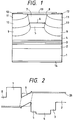
- FIG. 1 A first embodiment of the present invention will be described with reference to Fig. 1.
- an SiO2 film was formed on the above layers by vacuum vapor deposition.
- the SiO2 film was made in the form of a stripe having a width of about 5 ⁇ m using the known photolithography.
- a reverse mesa structure having a depth of about 2.5 ⁇ m was then formed using a phosphoric acid based etching solution.
- This sample was then dipped in a (NH4)2Sx solution for several min and cleaned by an alcohol based solvent, and it was put in the molecular beam epitaxy system again.
- This sample was heated at about 300°C to remove excessive sulfur.
- the SiO2 film was then removed using a fluoric acid based etching solution, and an SiO2 film 12 was formed on the sample by vacuum vapor deposition.
- a striped hole having a width of about 5 ⁇ m was opened in the SiO2 film 12 to the above stripe using the known photolithography.
- the sample was then dipped in the (NH4)2Sx solution for several min and cleaned with alcohol based solvent.
- a Ti-Pt-Au multi-layer electrode 13 was deposited to a thickness of about 1 ⁇ m by vacuum vapor deposition.
- an AuGe-Ni-Au multi-layer electrode 14 was deposited on the rear surface of the GaAs substrate which was polished to a thickness of 100 ⁇ m, after which the sample was cleaved to form a laser structure having a length of 400 ⁇ m.
- the device thus obtained was dipped in the (NH4)2Sx solution for several min and cleaned with alcohol based solvent.
- a ZnS-SiO2 multi-layer reflection film was then formed at the end surface of the resonator by sputtering.
- Numeral 26 designates the Fermi level.
- Positive holes injected by the p-type semiconductor layer are confined by an electric potential formed on the valency electron band side by the p-n junction and the junction between the Zn 0.8 Cd 0.2 S 0.4 Se 0.6 light guide layer and the Zn 0.8 Cd 0.2 S 0.1 Se 0.9 active layer.
- electrons injected from the n-type semiconductor are confined by an electric potential formed on the conducting band side by the p-n junction and the junction between the ZnS 0.1 Se 0.9 clad layer and the Zn 0.8 Cd 0.2 S 0.1 Se 0.9 active layer.
- the surface of the sample was then irradiated with molecular beams of Te for several tens min while keeping the sample temperature at the crystal growth temperature.
- a p-type ZnSeTe alloy having a gradient composition was formed on the surface of the sample.
- SiO2 film was formed on the sample by vacuum vapor deposition.
- the SiO2 film was made in the form of a stripe having a width of about 5 ⁇ m using the known photolithography.
- a reverse mesa structure having a depth of about 3.0 ⁇ m was then formed using a phosphoric acid based etching solution.
- the sample was then dipped in a (NH4)2Sx solution for several min and cleaned by an alcohol based solvent, and it was put in the molecular beam epitaxy system again.
- the sample was heated at about 300°C to remove excessive sulfur.
- the SiO2 film was then removed using a fluoric acid based etching solution, and an SiO2 film 12 was formed on the surface of the sample by vacuum vapor deposition.
- a striped hole having a width of about 5 ⁇ m was opened in the SiO2 film 12 to the above stripe using the known photolithography.
- the sample was then dipped in a (NH4)2Sx solution for several min and cleaned with alcohol based solvent.
- a Ti-Pt-Au multi-layer electrode 13 was deposited to a thickness of about 1 ⁇ m by vacuum vapor deposition.
- an AuGe-Ni-Au multi-layer electrode 14 was deposited on the rear surface of the GaAs substrate which was polished to a thickness of 100 ⁇ m, after which the sample was cleaved to form a laser structure having a length of 400 ⁇ m.
- the device thus obtained was dipped in the (NH4)2Sx solution for several min and cleaned with alcohol based solvent.
- An SiNx-SiCx multi-layer reflection film was then formed at the end surface of the resonator by plasma CVD.
- the ZnSe-Zn 0.8 Cd 0.2 Se supperlattice light guide layer used in this structure is shown in Fig. 4.
- numeral 27 designates ZnSe
- 28 is Zn 0.8 Cd 0.2 Se
- 29 is the lower end of an apparent conducting band
- 30 is the upper end of an apparent valency electron band.
- the structure in which the film thickness is gradually changed has the same effect as that of the alloy having the gradient composition.
- the laser of this structure has a band structure shown in Fig. 5.
- numeral 26 designates the Fermi level.
- SiO2 film was formed on the above layers by vacuum vapor deposition.
- the SiO2 film was made in the form of a stripe having a width of about 5 ⁇ m using the known photolithography.
- a reverse mesa structure having a depth of about 2.0 ⁇ m was then formed using a sulfuric acid based etching solution.
- This sample was then dipped in a (NH4)2Sx solution for several min and cleaned by an alcohol based solvent, and it was put in the molecular beam epitaxy system again.
- This sample was heated at about 300°C to remove excessive sulfur.
- an undoped MgS 0.9 Se 0.1 block layer 33 (n/p ⁇ 1 El5, 2.0 ⁇ m) was grown as a buried layer.
- the SiO2 film was then removed using a fluoric acid based etching solution, and an SiO2 film 12 was formed on the surface of the sample by vacuum vapor deposition.
- a striped hole having a width of about 5 ⁇ m was opened in the SiO2 film 12 to the above stripe using the known photolithography.
- the sample was then dipped in a (NH4)2Sx solution for several min and cleaned with alcohol based solvent.
- a Ti-Pt-Au multi-layer electrode 13 was deposited to a thickness of about 1 ⁇ m by vacuum vapor deposition.
- an AuGe-Ni-Au multi-layer electrode 25 was deposited on the rear surface of the GaAs substrate which was polished to a thickness of 100 ⁇ m, after which the sample was cleaved to form a laser structure having a length of 500 ⁇ m.
- the device thus obtained was dipped in the (NH4)2Sx solution for several min and cleaned with alcohol based solvent, and a SiO2-TiO2 multi-layer reflection film was formed at the end surface of the resonator by vacuum vapor deposition.
- the semiconductor laser device of this structure is capable of continuously oscillating a blue laser of a single vertical mode with an oscillation wavelength of about 450 nm at room temperature.
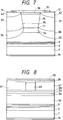
- a fourth embodiment of the present invention will be described with reference to Fig. 7.
- the surface of the sample was irradiated with molecular beams of Te for several tens min while keeping the sample temperature at the crystal growth temperature, and then was cooled to a temperature near room temperature.
- a p-type ZnSeTe alloy having a gradient composition was formed on the surface of the sample.
- an SiO2 film was formed on the sample by plasma CVD.
- the SiO2 film was made in the form of a stripe having a width of about 5 ⁇ m using the known photolithography.
- a reverse mesa structure having a depth of about 2 ⁇ m was then formed using a sulfuric acid based etching solution.
- This sample was then dipped in a (NH4)2Sx solution for several min and cleaned by an alcohol based solvent, and it was put in the metal-organic vapor deposition system.
- This sample was irradiated with hydrogen radicals while being heated at about 300°C to remove excessive sulfur.
- the SiO2 film was then removed using a fluoric acid based etching solution, and an SiO2 film 12 was formed on the sample by plasma CVD.
- a striped hole having a width of about 5 ⁇ m was opened in the SiO2 film 12 to the above stripe using the known photolithography.
- the sample was then dipped in a (NH4)2Sx solution for several min and cleaned with alcohol based solvent.
- a Ti-Pt-Au multi-layer electrode 13 was deposited to a thickness of about 1 ⁇ m by vacuum vapor deposition.
- an AuGe-Ni-Au multi-layer electrode 14 was deposited on the rear surface of the GaAs substrate which was polished to a thickness of 100 ⁇ m, after which the sample was cleaved to form a laser structure with a length of 400 ⁇ m.
- the device thus obtained was dipped in the (NH4)2Sx solution for several min and cleaned with alcohol based solvent, and a CaF2-SiO2 multi-layer reflection film was formed at the end surface of the resonator by sputtering.
- the semiconductor laser of this structure is capable of continuously oscillating at room temperature a marine blue laser of a single vertical mode having a characteristic of a threshold current of 50 mA, a drive voltage 4V, and an oscillation wavelength of 510 nm.
- a fifth embodiment of the present invention will be described with reference to Fig. 8.
- SiO2 film was formed on the above layers by plasma CVD.
- the SiO2 film was made in the form of a stripe having a width of about 5 ⁇ m using the known photolithography.
- a reverse mesa structure having a depth of about 1 ⁇ m was formed using a sulfuric acid based selective etching solution.
- This sample was then dipped in a (NH4)2Sx solution for several min and cleaned by an alcohol based solvent, and it was put in the metal-organic vapor deposition system.
- the sample was irradiated with hydrogen radicals while being heated at about 300°C to remove excessive sulfur.
- the SiO2 film was then removed using a fluoric acid based etching solution, and the sample was dipped in a (NH4)2Sx solution for several minutes and cleaned using an alcohol solvent, and it was put in the molecular beam epitaxy system.
- the surface of the sample was irradiated with molecular beams of Te for several tens min while keeping the sample temperature at the crystal growth temperature, and was then cooled to a temperature near room temperature. By this processing, a p-type ZnSeTe alloy having a gradient composition was formed on the surface of the sample.
- a Ti-Pt-Au multi-layer electrode 13 was deposited to a thickness of about 1 ⁇ m by vacuum vapor deposition.
- an AuGe-Ni-Au multi-layer electrode 14 was deposited on the rear surface of the GaAs substrate which was polished to a thickness of 100 ⁇ m, after which the sample was cleaved to form a laser structure having a length of 400 ⁇ m.
- the device thus obtained was dipped in the (NH4)2Sx solution for several min and cleaned with alcohol based solvent, and a ZnS-SiO2 multi-layer reflection film was formed at the end surface of the resonator by sputtering.
- the semiconductor laser of this structure is capable of continuously oscillating at room temperature a marine blue laser of a single vertical mode having a characteristic of a threshold current of 60 mA, a drive voltage 5V, and an oscillation wavelength of 450 nm.
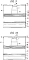
- a sixth embodiment of the present invention will be described with reference to Fig. 9.
- the surface of the sample was irradiated with molecular beams of Te for several tens min while keeping the sample temperature at the crystal growth temperature, and was then cooled to a temperature near room temperature.
- a p-type ZnSeTe alloy with a gradient composition was formed on the surface of the sample.
- an SiO2 film was formed on the sample by plasma CVD.
- the SiO2 film was made in the form of a stripe having a width of about 5 ⁇ m using the known photolithography.
- a reverse mesa structure having a depth of about 1.5 ⁇ m was then formed using a bromine based selective etching solution.
- the sample was then dipped in a (NH4)2Sx solution for several min and cleaned with an alcohol based solvent, and it was put in the metal-organic vapor deposition system.
- This sample was irradiated with hydrogen radicals while being heated at about 300°C to remove excessive sulfur.
- an SiO2 film 12 was formed on the buried layer by plasma CVD, and a striped hole having a width of about 5 ⁇ m was formed in the SiO2 film using the known photolithography.
- a Ti-Pt-Au multi-layer electrode 13 was deposited to a thickness of about 1 ⁇ m by vacuum vapor deposition.
- an AuGe-Ni-Au multi-layer electrode 14 was deposited on the rear surface of the GaAs substrate which was polished to a thickness of 100 ⁇ m, after which the sample was cleaved to form a laser structure having a length of 1000 ⁇ m.
- the device thus obtained was dipped in the (NH4)2Sx solution for several min and cleaned with alcohol based solvent, and an SiNx-SiO2 multi-layer reflection film was formed at the end surface of the resonator by sputtering.
- the semiconductor laser of this structure is capable of continuously oscillating at room temperature a marine blue laser of a single vertical mode having a characteristic of a threshold current of 2 mA, a drive voltage 4V, and an oscillation wavelength of 500 nm.
- a seventh embodiment of the present invention will be described with reference to Fig. 10.
- the surface of the sample was irradiated with molecular beams of Te for several tens min while keeping the sample temperature of at the crystal growth temperature, and was then cooled to a temperature near room temperature.
- a p-type ZnSeTe alloy with a gradient composition was formed on the surface of the sample.
- an SiO2 film was formed on the sample by plasma CVD.
- the SiO2 film was made in the form of a stripe having a width of about 5 ⁇ m using the known photolithography.
- a reverse mesa structure having a depth of about 1.5 ⁇ m was formed using a bromine based selective etching solution.
- This sample was then dipped in a (NH4)2Sx solution for several min and cleaned with an alcohol based solvent, and it was put in the metal-organic vapor deposition system.
- This sample was irradiated with hydrogen radicals while being heated at about 300°C to remove excessive sulfur.
- an SiO2 film 12 was formed on the buried layer by plasma CVD, and a striped hole having a width of about 5 ⁇ m was formed in the SiO2 film using the known photolithography.
- a Ti-Pt-Au multi-layer electrode 13 was deposited to a thickness of about 1 ⁇ m by vacuum vapor deposition.
- an AuGe-Ni-Au multi-layer electrode 14 was deposited on the rear surface of the GaAs substrate which was polished to a thickness of 100 ⁇ m, after which the sample was cleaved to form a laser structure with a length of 1000 ⁇ m.
- the device thus obtained was dipped in the (NH4)2Sx solution for several min and cleaned with alcohol based solvent, and an SiNx-SiO2 multi-layer reflection film was formed at the end surface of the resonator by sputtering.
- the semiconductor laser of this structure is capable of continuously oscillating at room temperature a marine blue of a single vertical mode having a characteristic of a threshold current of 2 mA, a drive voltage 4V, and an oscillation wavelength of 500 nm.
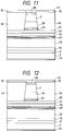
- a eighth embodiment of the present invention will be described with reference to Fig. 11.
- the surface of the sample was irradiated with molecular beams of Te for several tens min while keeping the sample temperature at the crystal growth temperature, and was then cooled to a temperature near room temperature.
- a p-type ZnSeTe alloy with a gradient composition was formed on the surface of the sample.
- an SiO2 film was formed on the above layers by plasma CVD.
- the SiO2 film was made in the form of a stripe having a width of about 5 ⁇ m using the known photolithography.
- a reverse mesa structure having a depth of about 1.5 ⁇ m was formed using a bromine based selective etching solution.
- This sample was then dipped in a (NH4)2Sx solution for several min and cleaned with an alcohol based solvent, and it was put in the metal-organic vapor deposition system.
- This sample was irradiated with hydrogen radicals while being heated at about 300°C to remove excessive sulfur.
- an SiO2 film 12 was formed on the buried layer by plasma CVD, and a striped hole having a width of about 5 ⁇ m was formed on the SiO2 film using the known photolithography.
- a Ti-Pt-Au multi-layer electrode 13 was deposited to a thickness of about 1 ⁇ m by vacuum vapor deposition.
- an AuGe-Ni-Au multi-layer electrode 14 was deposited on the rear surface of the GaAs substrate which was polished to a thickness of 100 ⁇ m, after which the sample was cleaved to form a laser structure with a length of 1000 ⁇ m.
- the device thus obtained was dipped in the (NH4)2Sx solution for several min and cleaned with alcohol based solvent, and an SiNx-SiO2 multi-layer reflection film was formed at the end surface of the resonator by sputtering.
- the semiconductor laser of this structure is capable of continuously oscillating at room temperature a marine blue laser of a single vertical mode having a characteristic of a threshold current of 2 mA, a drive voltage 4V, and an oscillation wavelength of 500 nm.
- a ninth embodiment of the present invention will be described with reference to Fig. 12.
- the surface of the sample was irradiated with molecular beams of Te for several tens min while keeping the sample temperature at the crystal growth temperature, and was then cooled to a temperature near room temperature.
- a p-type ZnSeTe alloy with a gradient composition was formed on the surface of the sample.
- an SiO2 film was formed on the sample by plasma CVD.
- the SiO2 film was made in the form of a stripe having a width of about 5 ⁇ m using the known photolithography.
- a reverse mesa structure having a depth of about 1.5 ⁇ m was formed using a bromine based selective etching solution.
- This sample was then dipped in a (NH4)2Sx solution for several min and cleaned by an alcohol based solvent, and it was put in the metal-organic vapor deposition system.
- the sample was irradiated with hydrogen radicals while being heated at about 300°C to remove excessive sulfur.
- an SiO2 film 12 was formed on the buried layer by plasma CVD, and a striped hole having a width of about 5 ⁇ m was formed in the SiO2 film using the known photolithography.
- a Ti-Pt-Au multi-layer electrode 13 was deposited to a thickness of about 1 ⁇ m by vacuum vapor deposition.
- an AuGe-Ni-Au multi-layer electrode 14 was deposited on the rear surface of the GaAs substrate which was polished to a thickness of 100 ⁇ m, after which the sample was cleaved to form a laser structure with a length of 1000 ⁇ m.
- the device thus obtained was dipped in the (NH4)2Sx solution for several min and cleaned with an alcohol based solvent, and an SiNx-SiO2 multi-layer reflection film was formed at the end surface of the resonator by sputtering.
- the semiconductor laser of this structure is capable of continuously oscillating at room temperature a marine blue laser of a single vertical mode having a characteristic of a threshold current of 2 mA, a drive voltage 4V, and an oscillation wavelength of 500 nm.
- a tenth embodiment of the present invention will be described with reference to Fig. 13.
- the surface of the sample was irradiated with molecular beams of Te for several tens min while keeping the sample temperature at the crystal growth temperature, and was then cooled to a temperature near room temperature.
- a p-type ZnSeTe alloy with a gradient composition was formed on the surface of the sample.
- An SiO2 film was formed on the sample by plasma CVD.
- the SiO2 film was made in the form of a stripe having a width of about 5 ⁇ m using the known photolithography.
- a reverse mesa structure having a depth of about 1.5 ⁇ m was formed using a bromine based selective etching solution.
- This sample was then dipped in a (NH4)2Sx solution for several min and cleaned by an alcohol based solvent, and it was put in the metal-organic vapor deposition system.
- This sample was irradiated with hydrogen radicals while being heated at about 300°C to remove excessive sulfur.
- an SiO2 film 12 was formed on the buried layer by plasma CVD, and a striped hole having a width of about 5 ⁇ m was formed on the SiO2 film using the known photolithography.
- a Ti-Pt-Au multi-layer electrode 13 was deposited to a thickness of about 1 ⁇ m by vacuum vapor deposition.
- an AuGe-Ni-Au multi-layer electrode 14 was deposited on the rear surface of the GaAs substrate which was polished to a thickness of 100 ⁇ m, after which the sample was cleaved to form a laser structure with a length of 1000 ⁇ m.
- the device thus obtained was dipped in the (NH4)2Sx solution for several min and cleaned with alcohol based solvent, and an SiNx-SiO2 multi-layer reflection film was formed at the end surface of the resonator by sputtering.
- the semiconductor laser of this structure is capable of continuously oscillating at room temperature a marine blue laser of a single vertical mode having a characteristic of a threshold current of 2 mA, a drive voltage 4V, and an oscillation wavelength of 500 nm.
- an eleventh embodiment of the present invention will be described with reference to Fig. 14.
- the surface of the sample was irradiated with molecular beams of Te for several tens min while keeping the sample temperature at the crystal growth temperature, and was then cooled to a temperature near room temperature.
- a p-type ZnSeTe alloy with a gradient composition was formed on the surface of the sample.
- An SiO2 film was formed on the sample by plasma CVD.
- the SiO2 film was made in the form of a stripe having a width of about 5 ⁇ m using the known photolithography.
- a reverse mesa structure having a depth of about 1.5 ⁇ m was formed using a bromine based selective etching solution.
- This sample was then dipped in a (NH4)2Sx solution for several min and cleaned by an alcohol based solvent, and it was put in the metal-organic vapor deposition system.
- This sample was irradiated with hydrogen radicals while being heated at about 300°C to remove excessive sulfur.
- an SiO2 film 12 was formed on the buried layer by plasma CVD, and a striped hole having a width of about 5 ⁇ m was formed on the SiO2 film using the known photolithography.
- a Ti-Pt-Au multi-layer electrode 13 was deposited to a thickness of about 1 ⁇ m by vacuum vapor deposition.
- an AuGe-Ni-Au multi-layer electrode 14 was deposited on the rear surface of the GaAs substrate which was polished to a thickness of 100 ⁇ m, after which the sample was cleaved to form a laser structure with a length of 1000 ⁇ m.
- the device thus obtained was dipped in the (NH4)2Sx solution for several min and cleaned with alcohol based solvent, and an SiNx-SiO2 multi-layer reflection film was formed at the end surface of the resonator by sputtering.
- the semiconductor laser of this structure is capable of continuously oscillating at room temperature a marine blue laser of a single vertical mode having a characteristic of a threshold current of 2 mA, a drive voltage 4V, and an oscillation wavelength of 500 nm.
- a twelfth embodiment of the present invention will be described with reference to Fig. 15.
- the surface of the sample was irradiated with molecular beams of Te for several tens min while keeping the sample temperature at the crystal growth temperature, and was then cooled to a temperature near room temperature.
- a p-type ZnSeTe alloy with a gradient composition was formed on the surface of the sample.
- An SiO2 film was formed on the sample by plasma CVD.
- the SiO2 film was made in the form of a stripe having a width of about 5 ⁇ m using the known photolithography.
- a reverse mesa structure having a depth of about 1.5 ⁇ m was formed using a bromine based selective etching solution.
- This sample was then dipped in a (NH4)2Sx solution for several min and cleaned by an alcohol based solvent, and it was put in the metal-organic vapor deposition system.
- This sample was irradiated with hydrogen radicals while being heated at about 300°C to remove excessive sulfur.
- an SiO2 film 12 was formed on the buried layer by plasma CVD, and a striped hole having a width of about 5 ⁇ m was formed on the SiO2 film using the known photolithography.
- a Ti-Pt-Au multi-layer electrode 13 was deposited to a thickness of about 1 ⁇ m by vacuum vapor deposition.
- an AuGe-Ni-Au multi-layer electrode 14 was deposited on the rear surface of the GaAs substrate which was polished to a thickness of 100 ⁇ m, after which the sample was cleaved to form a laser structure with a length of 1000 ⁇ m.
- the device thus obtained was dipped in the (NH4)2Sx solution for several min and cleaned with alcohol based solvent, and an SiNx-SiO2 multi-layer reflection film was formed at the end surface of the resonator by sputtering.
- the semiconductor laser of this structure is capable of continuously oscillating at room temperature a marine blue laser of a single vertical mode having a characteristic of a threshold current of 2 mA, a drive voltage 4V, and an oscillation wavelength of 500 nm.
- a thirteenth embodiment of the present invention will be described with reference to Fig. 16.
- the surface of the sample was irradiated with molecular beams of Te for several tens min while keeping the sample temperature at the crystal growth temperature, and was then cooled to a temperature near room temperature.
- a p-type ZnSeTe alloy with a gradient composition was formed on the surface of the sample.
- An SiO2 film was formed on the sample by plasma CVD.
- the SiO2 film was made in the form of a stripe having a width of about 5 ⁇ m using the known photolithography.
- a reverse mesa structure having a depth of about 1.5 ⁇ m was formed using a bromine based selective etching solution.
- This sample was then dipped in a (NH4)2Sx solution for several min and cleaned by an alcohol based solvent, and it was put in the metal-organic vapor deposition system.
- This sample was irradiated with hydrogen radicals while being heated at about 300°C to remove excessive sulfur.
- an SiO2 film 12 was formed on the buried layer by plasma CVD, and a striped hole having a width of about 5 ⁇ m was formed on the SiO2 film using the known photolithography.
- a Ti-Pt-Au multi-layer electrode 13 was deposited to a thickness of about 1 ⁇ m by vacuum vapor deposition.
- an AuGe-Ni-Au multi-layer electrode 14 was deposited on the rear surface of the GaAs substrate which was polished to a thickness of 100 ⁇ m, after which the sample was cleaved to form a laser structure with a length of 1000 ⁇ m.
- the device thus obtained was dipped in the (NH4)2Sx solution for several min and cleaned with alcohol based solvent, and an SiNx-SiO2 multi-layer reflection film was formed at the end surface of the resonator by sputtering.
- the semiconductor laser of this structure is capable of continuously oscillating at room temperature a marine blue laser of a single vertical mode having a characteristic of a threshold current of 2 mA, a drive voltage 4V, and an oscillation wavelength of 500 nm.
- a short wave II-VI compound semiconductor laser with a high reliability which is capable of reducing the threshold current, lowering the contact resistance of an electrode, and reducing the lattice strain due to thermal expansion; and which is capable of continuously oscillating a laser at room temperature by the improvement in the confinement of injected charge and light.
Abstract
Description
- The present invention relates to a semiconductor laser device, and particularly to a short wave semiconductor laser device composed of a II-VI compound semiconductor used for information processing terminal equipment such as an optical disk, laser beam printer or laser television, and a method of fabricating the laser device.
- A conventional semiconductor laser device using a II-VI compound semiconductor has a gain waveguiding type electrode stripe structure in which an alloy of ZnCdSSe or ZnMgSSe is grown on a GaAs substrate. The former structure using ZnCdSSe has been described, for example in Unexamined Japanese Patent Publication No. HEI 3-91270; and the latter structure using ZnMgSSe has been described, for example in Unexamined Japanese Patent Publication No. HEI 5-75217. In these structures, a continuous oscillation at low temperatures or a pulse oscillation at room temperature can be realized at an oscillation wavelength of about 500 nm (ZnCdSSe system) or about 450 nm (ZnMgSSe system).
- These structures, however, have the following disadvantages. The threshold current is relatively large because of the gain waveguiding type. It is difficult to form an ohmic contact with an electrode material because of the wide gap material. The thermal expansion strain remains in the device because a III-V compound semiconductor is used as a growth substrate. It is difficult to design a laser structure with a large band continuity between a clad layer and an active layer for the ZnCdSSe system being easy in the conducting control compared with the ZnMgSSe system, resulting in the insufficient confinement of injected charge and light. Because of these disadvantages, the above structures are difficult to achieve the continuous oscillation at room temperature and the operation with a high reliability.
- An object of the present invention is to provide a short wave semiconductor laser device composed of a II-VI compound semiconductor capable of solving the above-described problems.
- The present invention basically includes a buried type semiconductor laser structure using a II-VI compound semiconductor for reducing the threshold current and improving the reliability, wherein a multi-layer reflection film is provided for achieving the short wave oscillation. Concretely, in a buried type semiconductor laser device composed of a II-VI compound semiconductor, a buried layer is made of a II-VI compound semiconductor having a refraction factor lower than that of an active layer of the laser device. The buried layer has a forbidden band width larger than that of an active layer of the laser device. The buried layer has such a composition that the lattice constant thereof is substantially matched to that of a substrate on which the laser device is grown, and also it has an electric resistance high enough not to exert an effect on the operation of the laser composed of an n-type clad-active layer-a p-type clad. The buried layer is made of a II-VI compound semiconductor having a conducting type opposed to that of a clad layer being horizontally contacted with the surface of a substrate or to that of an active layer. The method of forming a buried layer includes the steps of: forming sulfur atoms or a layer of sulfur atoms on a II-VI compound semiconductor; introducing the II-VI compound semiconductor in a thin film deposition apparatus; removing the sulfur atoms or a layer of sulfur atoms by a suitable amount using electromagnetic wave, corpuscular beam, heat or solution; and growing or depositing a new material of a II-VI compound semiconductor, a III-V compound, a IV compound, a IV-VI compound, or a II-VII compound. At this time, the sulfur atoms or a layer of sulfur atoms formed on the II-VI compound semiconductor are removed at a temperature of 400°C or less, and a new material of a II-VI compound semiconductor, a III-V compound, a IV compound, a IV-VI compound, or a II-VII compound is grown or deposited on the exposed surface. A material, which is used for formation of a protection film or multi-layer reflection film at the end surface of a resonator, contains one kind or more of II-VI compounds having a forbidden band width larger than that of an active layer, such as ZnS or MgS; one kind or more of IV-VI compounds having a forbidden band width larger than that of an active layer, such as SiO₂ or TiO₂; one kind or more of II-VII compounds having a forbidden band width larger than that of an active layer, such as MgF₂ or CaF₂; or one kind or more of IV compounds having a forbidden band width larger than that of an active layer, such as C, SiCx or SiNx.
- To form an electrode having a small contact resistance on a p-type clad layer having a wide forbidden band width, a cap layer is made of a P-type CdSSe alloy having a small energy difference on the valency electron side to the clad layer and a relatively narrow forbidden band width. The cap layer made of an alloy with a gradient composition can be easily fabricated by exposing the surface of a clad layer to a molecular beam of Cd or Te. Namely, in forming an electrode to the II-VI compound semiconductor, a layer including an alloy of CdSSe is grown on the II-VI compound semiconductor as a cap layer, and then a metal film as an electrode is deposited on this layer. In this case, the II-VI compound semiconductor is exposed to a molecular beam or a gas containing Cd or Te in a crystal deposition apparatus, and a metal film as an electrode is deposited on the surface thereof.
- For reducing a strain generated in the device due to a large difference in a linear thermal expansion coefficient between a substrate of GaAs, that is, a III-V compound and a II-VI compound, a strain superlattice is introduced in the hetero-interface. Namely, in epitaxially growing a device composed of a II-VI compound semiconductor on a substrate made of a IV such as Si or a III-V compound semiconductor such as GaAs or InP, a strained supperlattice including at least one thin film of II-VI compound semiconductor is introduced in the hetero-interface as a region for reducing a strain caused by thermal expansion or contraction.
- To realize the sufficient confinement of injected charge in the ZnCdSSe based laser structure, there is provided an asymmetric double hetero structure in which the ZnSSe layer is used as the p-type clad layer and the ZnCdSSe layer is used as the n-type clad layer. Moreover, to sufficient confine a light, the ZnCdSSe based laser structure adopts a GRIN-SCH structure using a supperlattice with the film thickness gradually changed as a light confinement layer. Namely, a double hetero type semiconductor laser device using a II-VI compound semiconductor composed of an alloy of ZnMgCdSSe, includes an n-type clad layer, a p-type clad layer and an active layer, wherein each of said n-type and p-type clad layers has a lattice constant substantially matched to that of a substrate crystal or a buffer layer formed at the hetero-interface, and which has a forbidden band width larger than that of an active layer; said n-type and p-type clad layers are different in the alloy composition from each other; and the difference (


- In the present invention, a buried type laser structure enables the effective current constriction. Moreover, by provision of a refraction factor waveguiding type structure for waveguide of a light, it is possible to reduce the threshold current, and to improve the laser light characteristics. To fabricate the buried structure, the re-growth technique of the buried layer is required. However, by processing the surface of a II-VI compound forming the mesa structure with sulfur, it becomes possible to obtain the cleaned surface through heating at a temperature near the growth temperature of II-VI compound (400°C or less).
- Moreover, by forming a reflection multi-layer film or protection film not to absorb a short wave light on the end surface of the resonator, it is possible to reduce the threshold current, and to suppress the breakage of the end surface. In this case, by use of a thin film of ZnS or MgS excellent in adhesiveness, or a diamond based (poly-C, SiC) thin film having a high refraction factor and a resistance to deterioration, and by processing the end surface with sulfur prior to formation of these thin films, it becomes possible to obtain a high reliability.
- In the formation of an electrode on the p-type crystal, by coating the p-type crystal with the material of an alloy of CdSSe being small in the energy difference on the valency electron band side with respect to the p-type crystal, it becomes possible to effectively inject positive holes. On the other hand, when ZnTe being large in the energy difference on the valency electron band side and being easy to obtain the p-type conduction is used, an alloy with a gradient composition must be fabricated. According to the present invention, it becomes possible to easily fabricate such an alloy with a gradient composition.
- As a typical example, between a substrate of GaAs (III-V compound) and ZnSe or ZnS (II-VI compound), there is a mismatch in the thermal expansion coefficient of about 40%. Accordingly, even when the lattice constant of the ZnSSe alloy is matched to that of the GaAs substrate at the growth temperature of about 300°C, there is generated a lattice strain at room temperature where the device is used. To reduce the strain, by introducing, for example a ZnSe-ZnSSe strained superlattice in the hetero-interface, it becomes possible to suppress the propagation of the expansion or contraction of the substrate to the device, and hence to improve the reliability of the semiconductor laser.
- In a semiconductor laser of a ZnCdSSe system using clad layers having different alloy compositions, it is possible to achieve the lattice match to the substrate, and to effectively confine the injected charge. For example, when a ZnSSe alloy is used as the p-type clad layer, a ZnCdSe alloy is used as an active layer, and a ZnCdSSe alloy is used as an n-type clad layer, electrons can be confined by the electrical field formed in ZnSSe and positive holes can be confined by the electrical field formed in ZnCdSSe. Moreover, an asymmetric SCH structure is used to achieve the light confinement, wherein a ZnCdSSe n-type clad layer is used as a light guide layer, and an n-type ZnCdS alloy is used as a clad layer.
- On the other hand, in the recent structure including a clad layer of ZnSSe, an active layer of ZnCdSe, and a light guide layer of ZnSe, the film thickness of the light guide layer is required to be more than the critical film thickness of ZnSe for effectively confining a light. In this regard, lattice defects in ZnSe present a problem. To cope with this problem, a superlattice composed of ZnSe-ZnSSe with the film thickness gradually changed is used as the light guide layer. This makes it possible to obtain a film thickness enough to confine a light without any generation of lattice defects, and to easily fabricate a GRIN-SCH type semiconductor device using molecular beam epitaxy which is difficult to fabricate an alloy having a gradient composition.
-
- Fig. 1 is a semiconductor laser structure of a first embodiment of the present invention;
- Fig. 2 is a bad structure of the semiconductor laser of the first embodiment of the present invention;
- Fig. 3 is a semiconductor laser structure of a second embodiment of the present invention;
- Fig. 4 is a structure of a supperlattice light guide layer of the second embodiment of the present invention;
- Fig. 5 is a band structure of the semiconductor laser of the second embodiment of the present invention;
- Fig. 6 is a semiconductor laser structure of a third embodiment of the present invention;
- Fig. 7 is a semiconductor laser structure of a fourth embodiment of the present invention;
- Fig. 8 is a semiconductor laser structure of a fifth embodiment of the present invention;
- Fig. 9 is a semiconductor laser structure of a sixth embodiment of the present invention;
- Fig. 10 is a semiconductor laser structure of a seventh embodiment of the present invention;
- Fig. 11 is a semiconductor laser structure of an eighth embodiment of the present invention;
- Fig. 12 is a semiconductor laser structure of a ninth embodiment of the present invention;
- Fig. 13 is a semiconductor laser structure of a tenth embodiment of the present invention;
- Fig. 14 is a semiconductor laser structure of an eleventh embodiment of the present invention;
- Fig. 15 is a semiconductor laser structure of a twelfth embodiment; and
- Fig. 16 is a semiconductor laser structure of a thirteenth embodiment of the present invention.
- A first embodiment of the present invention will be described with reference to Fig. 1. On an n-
type GaAs substrate 1, there were sequentially grown by molecular beam epitaxy, an Se doped GaAs buffer layer 2 (n = 1El8, 0.5 µm), a Cℓ doped ZnSe-ZnS0.2Se0.8 strained superlattice 3 (n = 5El8, 0.5 µm), a Cℓ doped Zn0.5Cd0.5S0.9Se0.1 clad layer 4 (n = 5El8, 1.5 µm), a Cℓ doped Zn0.8Cd0.2S0.4Se0.6 light guide layer 5 (n = 5El7, 0.5 µm), an undoped Zn0.8Cd0.2S0.1Se0.9 active layer 6 (0.01 µm), an N₂ doped ZnS0.1Se0.9 clad layer 7 (p = 1El8, 1.0 µm), and an N₂ doped CdSe cap layer 8 (p = 1El9, 0.01 µm). - Next, an SiO₂ film was formed on the above layers by vacuum vapor deposition. The SiO₂ film was made in the form of a stripe having a width of about 5 µm using the known photolithography. A reverse mesa structure having a depth of about 2.5 µm was then formed using a phosphoric acid based etching solution. This sample was then dipped in a (NH₄)₂Sx solution for several min and cleaned by an alcohol based solvent, and it was put in the molecular beam epitaxy system again.
- This sample was heated at about 300°C to remove excessive sulfur. On this sample, there were sequentially grown, as buried layers, an N₂ doped Zn0.5Cd0.5S0.9Se0.1 block layer 9 (p = 1El6, 1.5 µm), a Cℓ doped ZnS0.1Se0.9 block layer 10 (n = 1El6, 1.0 µm), and an N₂ doped ZnS0.1Se0.9 block layer 11 (p = 1El6, 0.5 µm). The SiO₂ film was then removed using a fluoric acid based etching solution, and an
SiO₂ film 12 was formed on the sample by vacuum vapor deposition. - Next, a striped hole having a width of about 5 µm was opened in the
SiO₂ film 12 to the above stripe using the known photolithography. The sample was then dipped in the (NH₄)₂Sx solution for several min and cleaned with alcohol based solvent. After that, a Ti-Pt-Au multi-layer electrode 13 was deposited to a thickness of about 1 µm by vacuum vapor deposition. Moreover, an AuGe-Ni-Au multi-layer electrode 14 was deposited on the rear surface of the GaAs substrate which was polished to a thickness of 100 µm, after which the sample was cleaved to form a laser structure having a length of 400 µm. - The device thus obtained was dipped in the (NH₄)₂Sx solution for several min and cleaned with alcohol based solvent. A ZnS-SiO₂ multi-layer reflection film was then formed at the end surface of the resonator by sputtering.
- The band structure of this structure in the laser oscillation state is shown in Fig. 2.
Numeral 26 designates the Fermi level. Positive holes injected by the p-type semiconductor layer are confined by an electric potential formed on the valency electron band side by the p-n junction and the junction between the Zn0.8Cd0.2S0.4Se0.6 light guide layer and the Zn0.8Cd0.2S0.1Se0.9 active layer. On the other hand, electrons injected from the n-type semiconductor are confined by an electric potential formed on the conducting band side by the p-n junction and the junction between the ZnS0.1Se0.9 clad layer and the Zn0.8Cd0.2S0.1Se0.9 active layer. Thus, this structure enables the laser oscillation at a wavelength of 490 nm. - A second embodiment of the present invention will be described with reference to Fig. 3. On an n-
type GaAs substrate 1, there were sequentially grown by molecular beam epitaxy, an Se doped GaAs buffer layer 2 (n = 1El8, 0.5 µm), a Cℓ doped ZnSe-ZnS0.2Se0.8 strained superlattice 3 (n = 1El8, 0.5 µm), a Cℓ doped ZnS0.1Se0.9 clad layer 15 (n = 1El8, 1.5 µm), a Cℓ doped ZnSe-Zn0.8Cd0.2Se supperlattice light guide layer 16 (n = 5El7, 0.5 µm), an undoped Zn0.8Cd0.2Se active layer 17 (0.01 µm), an N₂ doped ZnSe-Zn0.8Cd0.2Se supperlattice light guide layer 18 (p = 5El7, 0.5 µm), and an N₂ doped ZnS0.1Se0.9 clad layer 7 (p = 1El8, 1.5 µm). The surface of the sample was then irradiated with molecular beams of Te for several tens min while keeping the sample temperature at the crystal growth temperature. By this processing, a p-type ZnSeTe alloy having a gradient composition was formed on the surface of the sample. - An SiO₂ film was formed on the sample by vacuum vapor deposition. The SiO₂ film was made in the form of a stripe having a width of about 5 µm using the known photolithography. A reverse mesa structure having a depth of about 3.0 µm was then formed using a phosphoric acid based etching solution. The sample was then dipped in a (NH₄)₂Sx solution for several min and cleaned by an alcohol based solvent, and it was put in the molecular beam epitaxy system again.
- The sample was heated at about 300°C to remove excessive sulfur. On the sample, there were sequentially grown, as buried layers, an N₂ doped ZnS0.1Se0.9 block layer 19 (p = 1El6, 1.0 µm), a Cℓ doped ZnS0.1Se0.9 block layer 10 (n = 1El6, 1.5 µm), an N₂ doped ZnS0.1Se0.9 block layer 11 (p = 1El6, 0.5 µm). The SiO₂ film was then removed using a fluoric acid based etching solution, and an
SiO₂ film 12 was formed on the surface of the sample by vacuum vapor deposition. - Next, a striped hole having a width of about 5 µm was opened in the
SiO₂ film 12 to the above stripe using the known photolithography. The sample was then dipped in a (NH₄)₂Sx solution for several min and cleaned with alcohol based solvent. After that, a Ti-Pt-Au multi-layer electrode 13 was deposited to a thickness of about 1 µm by vacuum vapor deposition. Moreover, an AuGe-Ni-Au multi-layer electrode 14 was deposited on the rear surface of the GaAs substrate which was polished to a thickness of 100 µm, after which the sample was cleaved to form a laser structure having a length of 400 µm. - The device thus obtained was dipped in the (NH₄)₂Sx solution for several min and cleaned with alcohol based solvent. An SiNx-SiCx multi-layer reflection film was then formed at the end surface of the resonator by plasma CVD.
- The ZnSe-Zn0.8Cd0.2Se supperlattice light guide layer used in this structure is shown in Fig. 4. In this figure, numeral 27 designates ZnSe, 28 is Zn0.8Cd0.2Se, 29 is the lower end of an apparent conducting band, and 30 is the upper end of an apparent valency electron band. As shown in the figure, the structure in which the film thickness is gradually changed has the same effect as that of the alloy having the gradient composition. The laser of this structure has a band structure shown in Fig. 5. In this figure, numeral 26 designates the Fermi level. By provision such a GRIN-SCH type semiconductor laser, it is possible to eliminate lattice defects of the light guide layer which has conventionally presented a problem, and hence to improve the reliability of the device.
- A third embodiment of the present invention will be described with reference to Fig. 6. On an n-
type ZnSe substrate 20, there were sequentially grown by molecular beam epitaxy, a Cℓ doped ZnSe buffer layer 21 (n = 1El8, 0.5 µm), a Cℓ doped Mg0.2Zn0.8S0.3Se0.7 clad layer 39 (n = 1El8, 1.0 µm), a Cℓ doped Zn0.9Cd0.1S0.2Se0.8 light guide layer 31 (n = 5El7, 0.5 µm), an undoped ZnSe active layer 23 (0.2 µm), an N₂ doped ZnS0.9Cd0.1S0.2Se0.8 light guide layer 32 (p = 5El7, 0.5 µm), an N₂ doped Mg0.2Zn0.8S0.3Se0.7 clad layer 40 (p = 1El8, 1.0 µm), and an N₂ doped CdSe cap layer 8 (p = 1El9, 0.01 µm). - An SiO₂ film was formed on the above layers by vacuum vapor deposition. The SiO₂ film was made in the form of a stripe having a width of about 5 µm using the known photolithography. A reverse mesa structure having a depth of about 2.0 µm was then formed using a sulfuric acid based etching solution. This sample was then dipped in a (NH₄)₂Sx solution for several min and cleaned by an alcohol based solvent, and it was put in the molecular beam epitaxy system again.
- This sample was heated at about 300°C to remove excessive sulfur. On this sample, an undoped MgS0.9Se0.1 block layer 33 (n/p < 1 El5, 2.0 µm) was grown as a buried layer. The SiO₂ film was then removed using a fluoric acid based etching solution, and an
SiO₂ film 12 was formed on the surface of the sample by vacuum vapor deposition. - Next, a striped hole having a width of about 5 µm was opened in the
SiO₂ film 12 to the above stripe using the known photolithography. The sample was then dipped in a (NH₄)₂Sx solution for several min and cleaned with alcohol based solvent. After that, a Ti-Pt-Au multi-layer electrode 13 was deposited to a thickness of about 1 µm by vacuum vapor deposition. Moreover, an AuGe-Ni-Au multi-layer electrode 25 was deposited on the rear surface of the GaAs substrate which was polished to a thickness of 100 µm, after which the sample was cleaved to form a laser structure having a length of 500 µm. - The device thus obtained was dipped in the (NH₄)₂Sx solution for several min and cleaned with alcohol based solvent, and a SiO₂-TiO₂ multi-layer reflection film was formed at the end surface of the resonator by vacuum vapor deposition.
- The semiconductor laser device of this structure is capable of continuously oscillating a blue laser of a single vertical mode with an oscillation wavelength of about 450 nm at room temperature.
- A fourth embodiment of the present invention will be described with reference to Fig. 7. On an n-
type GaAs substrate 1, there were sequentially grown by molecular beam epitaxy, an Se doped GaAs buffer layer 2 (n = 1El8, 0.5 µm), a Cℓ doped ZnSe-ZnS0.2Se0.8 strained superlattice 3 (n = 1El8, 0.5 µm), a Cℓ doped Mg0.1Zn0.9S0.2Se0.8 clad layer 22 (n = 1El8, 1.5 µm), a Cℓ doped ZnS0.1Se0.9 light guide layer 34 (n = 5El7, 0.3 µm), an undoped Zn0.8Cd0.2Se active layer 17 (0.01 µm), an N₂ doped ZnS0.1Se0.9 light guide layer 35 (p = 5El7, 0.3 µm), an N₂ doped Mg0.1Zn0.9S0.2Se0.8 clad layer 24 (p = 1El8, 1.0 µm), and an N₂ doped ZnSe cap layer 38 (p = 5El8, 0.1 µm). The surface of the sample was irradiated with molecular beams of Te for several tens min while keeping the sample temperature at the crystal growth temperature, and then was cooled to a temperature near room temperature. By this processing, a p-type ZnSeTe alloy having a gradient composition was formed on the surface of the sample. - Next, an SiO₂ film was formed on the sample by plasma CVD. The SiO₂ film was made in the form of a stripe having a width of about 5 µm using the known photolithography. A reverse mesa structure having a depth of about 2 µm was then formed using a sulfuric acid based etching solution. This sample was then dipped in a (NH₄)₂Sx solution for several min and cleaned by an alcohol based solvent, and it was put in the metal-organic vapor deposition system.
- This sample was irradiated with hydrogen radicals while being heated at about 300°C to remove excessive sulfur. On this sample, there were sequentially grown, as buried layers, an N₂ doped Mg0.2Zn0.8S0.3Se0.7 block layer 36 (p = 1El6, 1.0 µm), a Cℓ doped Mg0.2Zn0.8S0.3Se0.7 block layer 37 (n = 1El6, 1.0 µm), an N₂ doped Mg0.2Zn0.8S0.3Se0.7 block layer 42 (p = 1El6, 0.5 µm). The SiO₂ film was then removed using a fluoric acid based etching solution, and an
SiO₂ film 12 was formed on the sample by plasma CVD. - Next, a striped hole having a width of about 5 µm was opened in the
SiO₂ film 12 to the above stripe using the known photolithography. The sample was then dipped in a (NH₄)₂Sx solution for several min and cleaned with alcohol based solvent. After that, a Ti-Pt-Au multi-layer electrode 13 was deposited to a thickness of about 1 µm by vacuum vapor deposition. Moreover, an AuGe-Ni-Au multi-layer electrode 14 was deposited on the rear surface of the GaAs substrate which was polished to a thickness of 100 µm, after which the sample was cleaved to form a laser structure with a length of 400 µm. - The device thus obtained was dipped in the (NH₄)₂Sx solution for several min and cleaned with alcohol based solvent, and a CaF₂-SiO₂ multi-layer reflection film was formed at the end surface of the resonator by sputtering.
- The semiconductor laser of this structure is capable of continuously oscillating at room temperature a marine blue laser of a single vertical mode having a characteristic of a threshold current of 50 mA, a drive voltage 4V, and an oscillation wavelength of 510 nm.
- A fifth embodiment of the present invention will be described with reference to Fig. 8. On an n-
type GaAs substrate 1, there were sequentially grown by molecular beam epitaxy, an Se doped GaAs buffer layer 2 (n = 1El8, 0.5 µm), a Cℓ doped ZnSe-ZnS0.2Se0.8 strained superlattice 3 (n = 1El8, 0.5 µm), a Cℓ doped Mg0.2Zn0.8S0.3Se0.7 clad layer 39 (n=1El8, 1.5 µm), a Cℓ doped ZnS0.1Se0.9 light guide layer 34 (n = 5El7, 0.3 µm), an undoped ZnSe active layer 23 (0.1 µm), an N₂ doped ZnS0.1Se0.9 light guide layer 35 (p = 5El8, 0.3 µm), an N₂ doped Mg0.2Zn0.8S0.3Se0.7 clad layer 40 (p = 1El8, 1.0 µm), and an N₂ doped ZnSe cap layer 38 (p = 5El8, 0.05 µm). Next, an SiO₂ film was formed on the above layers by plasma CVD. The SiO₂ film was made in the form of a stripe having a width of about 5 µm using the known photolithography. A reverse mesa structure having a depth of about 1 µm was formed using a sulfuric acid based selective etching solution. This sample was then dipped in a (NH₄)₂Sx solution for several min and cleaned by an alcohol based solvent, and it was put in the metal-organic vapor deposition system. - The sample was irradiated with hydrogen radicals while being heated at about 300°C to remove excessive sulfur. On this sample, a Cℓ doped Mg0.3Zn0.7S0.4Se0.6 block layer 41 (n = 1El6, 1.0 µm) was grown as a buried layer. The SiO₂ film was then removed using a fluoric acid based etching solution, and the sample was dipped in a (NH₄)₂Sx solution for several minutes and cleaned using an alcohol solvent, and it was put in the molecular beam epitaxy system.
- The sample was irradiated with hydrogen radicals while being heated at about 300°C to remove excessive sulfur, and an N₂ doped ZnSe cap layer 38 (p = 5El8, 0.1 µm) was grown on the this sample. The surface of the sample was irradiated with molecular beams of Te for several tens min while keeping the sample temperature at the crystal growth temperature, and was then cooled to a temperature near room temperature. By this processing, a p-type ZnSeTe alloy having a gradient composition was formed on the surface of the sample.
- Next, a Ti-Pt-
Au multi-layer electrode 13 was deposited to a thickness of about 1 µm by vacuum vapor deposition. Moreover, an AuGe-Ni-Au multi-layer electrode 14 was deposited on the rear surface of the GaAs substrate which was polished to a thickness of 100 µm, after which the sample was cleaved to form a laser structure having a length of 400 µm. - The device thus obtained was dipped in the (NH₄)₂Sx solution for several min and cleaned with alcohol based solvent, and a ZnS-SiO₂ multi-layer reflection film was formed at the end surface of the resonator by sputtering.
- The semiconductor laser of this structure is capable of continuously oscillating at room temperature a marine blue laser of a single vertical mode having a characteristic of a threshold current of 60 mA, a drive voltage 5V, and an oscillation wavelength of 450 nm.
- A sixth embodiment of the present invention will be described with reference to Fig. 9. On an n-
type GaAs substrate 1, there were sequentially grown by molecular beam epitaxy, an Se doped GaAs buffer layer 2 (n = 1El8, 0.5 µm), a strained supperlattice 47 (n = 1El8, 0.03 µm) of five cycles of Cℓ doped ZnS0.1Se0.9 (5 nm) - Zn0.7Cd0.3S0.1Se0.9 (5 nm), a Cℓ doped Mg0.1Zn0.9S0.2Se0.8 clad layer 22 (n = 1El8, 1.5 µm), a supperlattice light guide layer 43 (n = 5El7, 0.1 µm) of seven cycles of Cℓ doped ZnS0.1Se0.9 (10 nm) - Zn0.7Cd0.3S0.1Se0.9 (3 nm), an undoped Zn0.7Cd0.3Se active layer 44 (0.01 µm), a supperlattice light guide layer 45 (p = 5El7, 0.1 µm) of seven cycles of N₂ doped ZnS0.1Se0.9 (10 nm) - Zn0.7Cd0.3S0.1Se0.9 (3 nm), an N₂ doped Mg0.1Zn0.9S0.2Se0.8 clad layer 24 (p = 1El7, 1.0 µm), an N₂ doped ZnS0.1Se0.9 clad layer 7 (p = 5El7, 0.5 µm), and a ZnSe cap layer 38 (p = 1El8, 0.1 µm). The surface of the sample was irradiated with molecular beams of Te for several tens min while keeping the sample temperature at the crystal growth temperature, and was then cooled to a temperature near room temperature. By this processing, a p-type ZnSeTe alloy with a gradient composition was formed on the surface of the sample. Next, an SiO₂ film was formed on the sample by plasma CVD. The SiO₂ film was made in the form of a stripe having a width of about 5 µm using the known photolithography. A reverse mesa structure having a depth of about 1.5 µm was then formed using a bromine based selective etching solution. The sample was then dipped in a (NH₄)₂Sx solution for several min and cleaned with an alcohol based solvent, and it was put in the metal-organic vapor deposition system. - This sample was irradiated with hydrogen radicals while being heated at about 300°C to remove excessive sulfur. On this sample, an undoped Mg0.2Zn0.7S0.3Se0.7 block layer 46 (n = 1El4, 1.5 µm) was grown as a buried layer. Next, an
SiO₂ film 12 was formed on the buried layer by plasma CVD, and a striped hole having a width of about 5 µm was formed in the SiO₂ film using the known photolithography. - Next, a Ti-Pt-
Au multi-layer electrode 13 was deposited to a thickness of about 1 µm by vacuum vapor deposition. Moreover, an AuGe-Ni-Au multi-layer electrode 14 was deposited on the rear surface of the GaAs substrate which was polished to a thickness of 100 µm, after which the sample was cleaved to form a laser structure having a length of 1000 µm. - The device thus obtained was dipped in the (NH₄)₂Sx solution for several min and cleaned with alcohol based solvent, and an SiNx-SiO₂ multi-layer reflection film was formed at the end surface of the resonator by sputtering.
- The semiconductor laser of this structure is capable of continuously oscillating at room temperature a marine blue laser of a single vertical mode having a characteristic of a threshold current of 2 mA, a drive voltage 4V, and an oscillation wavelength of 500 nm.
- A seventh embodiment of the present invention will be described with reference to Fig. 10. On an n-
type GaAs substrate 1, there were sequentially grown by molecular beam epitaxy, an Se doped GaAs buffer layer 2 (n = 1 El8, 0.5 µm), a strained supperlattice 3 (n = 1El8, 0.03 µm) of five cycles of Cℓ doped ZnS0.1Se0.9 (5 nm) - ZnSe (5 nm), a Cℓ doped Mg0.1Zn0.9S0.2Se0.8 clad layer 22 (n = 1El8, 1.5 µm), a supperlattice light guide layer 48 (n = 5El7, 0.1 µm) of ten cycles of Cℓ doped ZnS0.1Se0.9 (5 nm) - ZnSe (5 nm), an undoped Zn0.7Cd0.3Se active layer 44 (0.01 µm), a supperlattice light guide layer 49 (p = 5El7, 0.1 µm) of ten cycles of N₂ doped ZnS0.1Se0.9 (5 nm) - ZnSe (5 nm), an N₂ doped Mg0.1Zn0.9S0.2Se0.8 clad layer 24 (p = 1El7, 1.0 µm), an N₂ doped ZnS0.1S0.9 clad layer 7 (p = 5El7, 0.5 µm), and a ZnSe cap layer 38 (p = 1El8, 0.1 µm). The surface of the sample was irradiated with molecular beams of Te for several tens min while keeping the sample temperature of at the crystal growth temperature, and was then cooled to a temperature near room temperature. By this processing, a p-type ZnSeTe alloy with a gradient composition was formed on the surface of the sample. Next, an SiO₂ film was formed on the sample by plasma CVD. The SiO₂ film was made in the form of a stripe having a width of about 5 µm using the known photolithography. A reverse mesa structure having a depth of about 1.5 µm was formed using a bromine based selective etching solution. This sample was then dipped in a (NH₄)₂Sx solution for several min and cleaned with an alcohol based solvent, and it was put in the metal-organic vapor deposition system. - This sample was irradiated with hydrogen radicals while being heated at about 300°C to remove excessive sulfur. On this sample, an undoped Mg0.2Zn0.7S0.3Se0.7 block layer 46 (n = 1El4, 1.5 µm) was grown as a buried layer. Next, an
SiO₂ film 12 was formed on the buried layer by plasma CVD, and a striped hole having a width of about 5 µm was formed in the SiO₂ film using the known photolithography. - Next, a Ti-Pt-
Au multi-layer electrode 13 was deposited to a thickness of about 1 µm by vacuum vapor deposition. Moreover, an AuGe-Ni-Au multi-layer electrode 14 was deposited on the rear surface of the GaAs substrate which was polished to a thickness of 100 µm, after which the sample was cleaved to form a laser structure with a length of 1000 µm. - The device thus obtained was dipped in the (NH₄)₂Sx solution for several min and cleaned with alcohol based solvent, and an SiNx-SiO₂ multi-layer reflection film was formed at the end surface of the resonator by sputtering.
- The semiconductor laser of this structure is capable of continuously oscillating at room temperature a marine blue of a single vertical mode having a characteristic of a threshold current of 2 mA, a drive voltage 4V, and an oscillation wavelength of 500 nm.
- A eighth embodiment of the present invention will be described with reference to Fig. 11. On an n-
type GaAs substrate 1, there were sequentially grown by molecular beam epitaxy, an Se doped GaAs buffer layer 2 (n = 1El8, 0.5 µm), a Cℓ doped ZnS0.1Se0.9 clad layer 15 (n = 1 El8, 0.1 µm), a Cℓ doped Mg0.1Zn0.9S0.2Se0.8 clad layer 22 (n = 1El8, 1.5 µm), a supperlattice light guide layer 43 (n = 5El7, 0.1 µm) of seven cycles of Cℓ doped ZnS0.1Se0.9 (10 nm) - Zn0.7Cd0.3S0.1Se0.9 (3 nm), a Cℓ doped ZnS0.1Se0.9 light guide layer 34 (n = 5El7, 0.1 µm), an undoped Zn0.7Cd0.3Se active layer 44 (0.01 µm), an N₂ doped ZnS0.1Se0.9 light guide layer 35 (p = 5El7, 0.1 µm), a supperlattice light guide layer 45 (n = 5El7, 0.1 µm) of seven cycles of N₂ doped ZnS0.1Se0.9 (10 nm) - Zn0.7Cd0.3S0.1Se0.9 (3 nm), an N₂ doped Mg0.1Zn0.9S0.2Se0.8 clad layer 24 (p = 1El7, 1.0 µm), an N₂ doped ZnS0.1Se0.9 clad layer 7 (p = 5El7, 0.5 µm), and a ZnSe cap layer 38 (p = 1El8, 0.1 µm). The surface of the sample was irradiated with molecular beams of Te for several tens min while keeping the sample temperature at the crystal growth temperature, and was then cooled to a temperature near room temperature. By this processing, a p-type ZnSeTe alloy with a gradient composition was formed on the surface of the sample. Next, an SiO₂ film was formed on the above layers by plasma CVD. The SiO₂ film was made in the form of a stripe having a width of about 5 µm using the known photolithography. A reverse mesa structure having a depth of about 1.5 µm was formed using a bromine based selective etching solution. This sample was then dipped in a (NH₄)₂Sx solution for several min and cleaned with an alcohol based solvent, and it was put in the metal-organic vapor deposition system. - This sample was irradiated with hydrogen radicals while being heated at about 300°C to remove excessive sulfur. On this sample, an undoped Mg0.2Zn0.7S0.3Se0.7 block layer 46 (n = 1El4, 1.5 µm) was grown as a buried layer. Next, an
SiO₂ film 12 was formed on the buried layer by plasma CVD, and a striped hole having a width of about 5 µm was formed on the SiO₂ film using the known photolithography. - Next, a Ti-Pt-
Au multi-layer electrode 13 was deposited to a thickness of about 1 µm by vacuum vapor deposition. Moreover, an AuGe-Ni-Au multi-layer electrode 14 was deposited on the rear surface of the GaAs substrate which was polished to a thickness of 100 µm, after which the sample was cleaved to form a laser structure with a length of 1000 µm. - The device thus obtained was dipped in the (NH₄)₂Sx solution for several min and cleaned with alcohol based solvent, and an SiNx-SiO₂ multi-layer reflection film was formed at the end surface of the resonator by sputtering.
- The semiconductor laser of this structure is capable of continuously oscillating at room temperature a marine blue laser of a single vertical mode having a characteristic of a threshold current of 2 mA, a drive voltage 4V, and an oscillation wavelength of 500 nm.
- A ninth embodiment of the present invention will be described with reference to Fig. 12. On an n-
type GaAs substrate 1, there were sequentially grown by molecular beam epitaxy, an Se doped GaAs buffer layer 2 (n = 1El8, 0.5 µm), a Cℓ doped ZnS0.1Se0.9 clad layer 15 (n = 1El8, 0.1 µm), a Cℓ doped Mg0.1Zn0.9S0.2Se0.8 clad layer 22 (n = 1El8, 1.5 µm), a strained supperlattice light guide layer 48 (n = 5El7, 0.1 µm) of ten cycles of Cℓ doped ZnS0.1Se0.9 (5 nm) - ZnSe (5 nm), a Cℓ doped ZnS0.1Se0.9 light guide layer 34 (n = 5El7, 0.1 µm), an undoped Zn0.7Cd0.3Se active layer 44 (0.01 µm), an N₂ doped ZnS0.1Se0.9 light guide layer 43 (p = 5El7, 0.1 µm), a supperlattice light guide layer 49 (p = 5El7, 0.1 µm) of ten cycles of N₂ doped ZnS0.1Se0.9 (5 nm) - ZnSe (5 nm), an N₂ doped Mg0.1Zn0.9S0.2Se0.8 clad layer 24 (p = 1El7, 1.0 µm), an N₂ doped ZnS0.1Se0.9 clad layer 7 (p = 5El7, 0.5 µm), and a ZnSe cap layer 38 (p = 1El8, 0.1 µm). The surface of the sample was irradiated with molecular beams of Te for several tens min while keeping the sample temperature at the crystal growth temperature, and was then cooled to a temperature near room temperature. By this processing, a p-type ZnSeTe alloy with a gradient composition was formed on the surface of the sample. Next, an SiO₂ film was formed on the sample by plasma CVD. The SiO₂ film was made in the form of a stripe having a width of about 5 µm using the known photolithography. A reverse mesa structure having a depth of about 1.5 µm was formed using a bromine based selective etching solution. This sample was then dipped in a (NH₄)₂Sx solution for several min and cleaned by an alcohol based solvent, and it was put in the metal-organic vapor deposition system. - The sample was irradiated with hydrogen radicals while being heated at about 300°C to remove excessive sulfur. On this sample, an undoped Mg0.2Zn0.7S0.3Se0.7 block layer 46 (n = 1El4, 1.5 µm) was grown as a buried layer. Next, an
SiO₂ film 12 was formed on the buried layer by plasma CVD, and a striped hole having a width of about 5 µm was formed in the SiO₂ film using the known photolithography. - Next, a Ti-Pt-
Au multi-layer electrode 13 was deposited to a thickness of about 1 µm by vacuum vapor deposition. Moreover, an AuGe-Ni-Au multi-layer electrode 14 was deposited on the rear surface of the GaAs substrate which was polished to a thickness of 100 µm, after which the sample was cleaved to form a laser structure with a length of 1000 µm. - The device thus obtained was dipped in the (NH₄)₂Sx solution for several min and cleaned with an alcohol based solvent, and an SiNx-SiO₂ multi-layer reflection film was formed at the end surface of the resonator by sputtering.
- The semiconductor laser of this structure is capable of continuously oscillating at room temperature a marine blue laser of a single vertical mode having a characteristic of a threshold current of 2 mA, a drive voltage 4V, and an oscillation wavelength of 500 nm.
- A tenth embodiment of the present invention will be described with reference to Fig. 13. On an n-
type GaAs substrate 1, there were sequentially grown by molecular beam epitaxy, an Se doped GaAs buffer layer 2 (n = 1El8, 0.5 µm), a Cℓ doped ZnS0.1Se0.9 clad layer 15 (n = 1El8, 0.1 µm), a Cℓ doped Mg0.1Zn0.9S0.2Se0.8 clad layer 22 (n = 1El8, 0.5 µm), a strained supperlattice 47 (n = 5El7, 0.07 µm) of five cycles of Cℓ doped ZnS0.1Se0.9 (10 nm) - Zn0.7Cd0.3S0.1Se0.9 (3 nm), a Cℓ doped Mg0.1Zn0.9S0.2Se0.8 clad layer 22 (n = 1El8, 1.0 µm), a Cℓ doped ZnS0.1Se0.9 light guide layer 34 (n = 5 El7, 0.1 µm), an undoped Zn0.7Cd0.3Se active layer 44 (0.01 µm), an N₂ doped ZnS0.1Se0.9 light guide layer 35 (p = 5El7, 0.1 µm), an undoped Mg0.1Zn0.9S0.2Se0.8 clad layer 24 (p = 1El7, 1.0 µm), an N₂ doped ZnS0.1Se0.9 cladlayer 7, and a ZnSe cap layer 38 (p = 1El8, 0.1 µm). The surface of the sample was irradiated with molecular beams of Te for several tens min while keeping the sample temperature at the crystal growth temperature, and was then cooled to a temperature near room temperature. By this processing, a p-type ZnSeTe alloy with a gradient composition was formed on the surface of the sample. An SiO₂ film was formed on the sample by plasma CVD. The SiO₂ film was made in the form of a stripe having a width of about 5 µm using the known photolithography. A reverse mesa structure having a depth of about 1.5 µm was formed using a bromine based selective etching solution. This sample was then dipped in a (NH₄)₂Sx solution for several min and cleaned by an alcohol based solvent, and it was put in the metal-organic vapor deposition system. - This sample was irradiated with hydrogen radicals while being heated at about 300°C to remove excessive sulfur. On the sample, an undoped Mg0.2Zn0.7S0.3Se0.7 block layer 46 (n = 1El4, 1.5 µm) was grown as a buried layer. Next, an
SiO₂ film 12 was formed on the buried layer by plasma CVD, and a striped hole having a width of about 5 µm was formed on the SiO₂ film using the known photolithography. - Next, a Ti-Pt-
Au multi-layer electrode 13 was deposited to a thickness of about 1 µm by vacuum vapor deposition. Moreover, an AuGe-Ni-Au multi-layer electrode 14 was deposited on the rear surface of the GaAs substrate which was polished to a thickness of 100 µm, after which the sample was cleaved to form a laser structure with a length of 1000 µm. - The device thus obtained was dipped in the (NH₄)₂Sx solution for several min and cleaned with alcohol based solvent, and an SiNx-SiO₂ multi-layer reflection film was formed at the end surface of the resonator by sputtering.
- The semiconductor laser of this structure is capable of continuously oscillating at room temperature a marine blue laser of a single vertical mode having a characteristic of a threshold current of 2 mA, a drive voltage 4V, and an oscillation wavelength of 500 nm.
- An eleventh embodiment of the present invention will be described with reference to Fig. 14. On an n-
type GaAs substrate 1, there were sequentially grown by molecular beam epitaxy, an Se doped GaAs buffer layer 2 (n = 1El8, 0.5 µm), a Cℓ doped ZnS0.1Se0.9 clad layer 15 (n = 1El8, 0.1 µm), a Cℓ doped Mg0.1Zn0.9S0.2Se0.8 clad layer 22 (n = 1El8, 0.5 µm), a strained supperlattice 3 (n = 5El7, 0.05 µm) of five cycles of Cℓ doped ZnS0.1Se0.9 (5 nm) - ZnSe (5 nm), a Cℓ doped Mg0.1Zn0.9S0.2Se0.8 clad layer 22 (n = 1El8, 0.5 µm), a Cℓ doped ZnS0.1Se0.9 light guide layer 34 (n = 5El7, 0.1 µm), an undoped Zn0.7Cd0.3Se active layer 44 (0.01 µm), an N₂ doped ZnS0.1Se0.9 light guide layer 43 (p = 5El7, 0.1 µm), an undoped Mg0.1Zn0.9S0.2Se0.8 clad layer 24 (p = 1El7, 1.0 µm), an N₂ doped ZnS0.1Se0.9 clad layer 7 (p = 5El7, 0.5 µm) and a ZnSe cap layer 38 (p = 1El8, 0.1 µm). The surface of the sample was irradiated with molecular beams of Te for several tens min while keeping the sample temperature at the crystal growth temperature, and was then cooled to a temperature near room temperature. By this processing, a p-type ZnSeTe alloy with a gradient composition was formed on the surface of the sample. An SiO₂ film was formed on the sample by plasma CVD. The SiO₂ film was made in the form of a stripe having a width of about 5 µm using the known photolithography. A reverse mesa structure having a depth of about 1.5 µm was formed using a bromine based selective etching solution. This sample was then dipped in a (NH₄)₂Sx solution for several min and cleaned by an alcohol based solvent, and it was put in the metal-organic vapor deposition system. - This sample was irradiated with hydrogen radicals while being heated at about 300°C to remove excessive sulfur. On the sample, an undoped Mg0.2Zn0.7S0.3Se0.7 block layer 46 (n = 1El4, 1.5 µm) was grown as a buried layer. Next, an
SiO₂ film 12 was formed on the buried layer by plasma CVD, and a striped hole having a width of about 5 µm was formed on the SiO₂ film using the known photolithography. - Next, a Ti-Pt-
Au multi-layer electrode 13 was deposited to a thickness of about 1 µm by vacuum vapor deposition. Moreover, an AuGe-Ni-Au multi-layer electrode 14 was deposited on the rear surface of the GaAs substrate which was polished to a thickness of 100 µm, after which the sample was cleaved to form a laser structure with a length of 1000 µm. - The device thus obtained was dipped in the (NH₄)₂Sx solution for several min and cleaned with alcohol based solvent, and an SiNx-SiO₂ multi-layer reflection film was formed at the end surface of the resonator by sputtering.
- The semiconductor laser of this structure is capable of continuously oscillating at room temperature a marine blue laser of a single vertical mode having a characteristic of a threshold current of 2 mA, a drive voltage 4V, and an oscillation wavelength of 500 nm.
- A twelfth embodiment of the present invention will be described with reference to Fig. 15. On an n-type GaAs substrate 1, there were sequentially grown by molecular beam epitaxy, an Se doped GaAs buffer layer 2 (n = 1El8, 0.5 µm), a Cℓ doped ZnS0.1Se0.9 clad layer 15 (n = 1El8, 0.1 µm), a Cℓ doped Mg0.1Zn0.9S0.2Se0.8 clad layer 22 (n = 1El8, 1.5 µm), a Cℓ doped ZnS0.1Se0.9 light guide layer 34 (n = 5El7, 0.5 µm), a supperlattice light guide 43 (n = 5El7, 0.01 µm) of Cℓ doped ZnS0.1Se0.9 (10 nm) - Zn0.7Cd0.3S0.1Se0.9 (3 nm), a Cℓ doped ZnS0.1Se0.9 light guide layer 34 (n = 5El7, 0.5 µm), an undoped Zn0.7Cd0.3Se active layer 44 (0.01 µm), an N₂ doped ZnS0.1Se0.9 light guide layer 35 (p = 5El7, 0.05 µm), a supperlattice light guide 45 (n = 5El7, 0.01 µm) of N₂ doped ZnS0.1Se0.9 (10 nm) - Zn0.7Cd0.3S0.1Se0.9 (3 nm), an N₂ doped ZnS0.1Se0.9 light guide layer 35 (p = 5El7, 0.05 µm), an N₂ doped Mg0.1Zn0.9S0.2Se0.8 clad layer 24 (p = 1El7, 1.0 µm), an N₂ doped ZnS0.1Se0.9 clad layer 7 (p = 5El7, 0.5 µm) and a ZnSe cap layer 38 (p = 1El8, 0.1 µm). The surface of the sample was irradiated with molecular beams of Te for several tens min while keeping the sample temperature at the crystal growth temperature, and was then cooled to a temperature near room temperature. By this processing, a p-type ZnSeTe alloy with a gradient composition was formed on the surface of the sample. An SiO₂ film was formed on the sample by plasma CVD. The SiO₂ film was made in the form of a stripe having a width of about 5 µm using the known photolithography. A reverse mesa structure having a depth of about 1.5 µm was formed using a bromine based selective etching solution. This sample was then dipped in a (NH₄)₂Sx solution for several min and cleaned by an alcohol based solvent, and it was put in the metal-organic vapor deposition system.
- This sample was irradiated with hydrogen radicals while being heated at about 300°C to remove excessive sulfur. On the sample, an undoped Mg0.2Zn0.7S0.3Se0.7 block layer 46 (n = 1El4, 1.5 µm) was grown as a buried layer. Next, an
SiO₂ film 12 was formed on the buried layer by plasma CVD, and a striped hole having a width of about 5 µm was formed on the SiO₂ film using the known photolithography. - Next, a Ti-Pt-
Au multi-layer electrode 13 was deposited to a thickness of about 1 µm by vacuum vapor deposition. Moreover, an AuGe-Ni-Au multi-layer electrode 14 was deposited on the rear surface of the GaAs substrate which was polished to a thickness of 100 µm, after which the sample was cleaved to form a laser structure with a length of 1000 µm. - The device thus obtained was dipped in the (NH₄)₂Sx solution for several min and cleaned with alcohol based solvent, and an SiNx-SiO₂ multi-layer reflection film was formed at the end surface of the resonator by sputtering.
- The semiconductor laser of this structure is capable of continuously oscillating at room temperature a marine blue laser of a single vertical mode having a characteristic of a threshold current of 2 mA, a drive voltage 4V, and an oscillation wavelength of 500 nm.
- A thirteenth embodiment of the present invention will be described with reference to Fig. 16. On an n-type GaAs substrate 1, there were sequentially grown by molecular beam epitaxy, an Se doped GaAs buffer layer 2 (n = 1El8, 0.5 µm), a Cℓ doped ZnS0.1Se0.9 clad layer 15 (n = 1El8, 0.1 µm), a Cℓ doped Mg0.1Zn0.9S0.2Se0.8 clad layer 22 (n = 1El8, 1.5 µm), a Cℓ doped ZnS0.1Se0.9 light guide layer 34 (n = 5El7, 0.5 µm), a supperlattice light guide 48 (n = 5El7, 0.01 µm) of Cℓ doped ZnS0.1Se0.9 (5 nm) - ZnSe (5 nm), a Cℓ doped ZnS0.1Se0.9 light guide layer 34 (n = 5El7, 0.5 µm), an undoped Zn0.7Cd0.3Se active layer 44 (0.01 µm), an N₂ doped ZnS0.1Se0.9 light guide layer 35 (p = 5El7, 0.05 µm), a supperlattice light guide 49 (p = 5El7, 0.01 µm) of N₂ doped ZnS0.1Se0.9 (5 nm) - ZnSe (5 nm), an N₂ doped ZnS0.1Se0.9 light guide layer 35 (p = 5El7, 0.05 µm), an N₂ doped Mg0.1Zn0.9S0.2Se0.8 clad layer 24 (p = 1El7, 1.0 µm), an N₂ doped ZnS0.1Se0.9 clad layer 7 (p = 5El7, 0.5 µm) and a ZnSe cap layer 38 (p = 1El8, 0.1 µm). The surface of the sample was irradiated with molecular beams of Te for several tens min while keeping the sample temperature at the crystal growth temperature, and was then cooled to a temperature near room temperature. By this processing, a p-type ZnSeTe alloy with a gradient composition was formed on the surface of the sample. An SiO₂ film was formed on the sample by plasma CVD. The SiO₂ film was made in the form of a stripe having a width of about 5 µm using the known photolithography. A reverse mesa structure having a depth of about 1.5 µm was formed using a bromine based selective etching solution. This sample was then dipped in a (NH₄)₂Sx solution for several min and cleaned by an alcohol based solvent, and it was put in the metal-organic vapor deposition system.
- This sample was irradiated with hydrogen radicals while being heated at about 300°C to remove excessive sulfur. On the sample, an undoped Mg0.2Zn0.7S0.3Se0.7 block layer 46 (n = 1El4, 1.5 µm) was grown as a buried layer. Next, an
SiO₂ film 12 was formed on the buried layer by plasma CVD, and a striped hole having a width of about 5 µm was formed on the SiO₂ film using the known photolithography. - Next, a Ti-Pt-
Au multi-layer electrode 13 was deposited to a thickness of about 1 µm by vacuum vapor deposition. Moreover, an AuGe-Ni-Au multi-layer electrode 14 was deposited on the rear surface of the GaAs substrate which was polished to a thickness of 100 µm, after which the sample was cleaved to form a laser structure with a length of 1000 µm. - The device thus obtained was dipped in the (NH₄)₂Sx solution for several min and cleaned with alcohol based solvent, and an SiNx-SiO₂ multi-layer reflection film was formed at the end surface of the resonator by sputtering.
- The semiconductor laser of this structure is capable of continuously oscillating at room temperature a marine blue laser of a single vertical mode having a characteristic of a threshold current of 2 mA, a drive voltage 4V, and an oscillation wavelength of 500 nm.
- According to the present invention, there can be provided a short wave II-VI compound semiconductor laser with a high reliability, which is capable of reducing the threshold current, lowering the contact resistance of an electrode, and reducing the lattice strain due to thermal expansion; and which is capable of continuously oscillating a laser at room temperature by the improvement in the confinement of injected charge and light.
Claims (30)
- A buried type semiconductor laser device comprising a II-VI compound semiconductor, wherein a buried layer (9 to 11, 19, 33, 37, 41, 42, 46) is made of a II-VI compound semiconductor having a refraction factor lower than that of an active layer (6, 17, 23, 44) of said laser device.
- A semiconductor laser device according to claim 1, wherein said buried layer is made of a II-VI compound semiconductor having a forbidden band width larger than that of an active layer of said laser device.
- A semiconductor laser device according to claim 1, wherein said buried layer is made of a II-VI compound semiconductor having such a composition that the lattice constant thereof is substantially matched to that of a substrate (1) on which said laser device is grown.
- A semiconductor laser device according to claim 1, wherein said buried layer is made of a II-VI compound semiconductor having an electric resistance high enough not to exert an effect on the operation of the laser composed of an n-type clad-active layer-a p-type clad (4-6-7, 15-17-18, 39-23-40, 22-17-24).
- A semiconductor laser device according to claim 1, wherein said buried layer is made of a II-VI compound semiconductor (9, 10) having a conducting type opposed to that of a clad layer (4, 7) being horizontally contacted with the surface of a substrate or to that of an active layer.
- A method of forming a thin film comprising the steps of:
forming sulfur atoms or a layer of sulfur atoms on a II-VI compound semiconductor;
introducing said II-VI compound semiconductor in a thin film deposition apparatus;
removing said sulfur atoms or a layer of sulfur atoms by a suitable amount using electromagnetic wave, corpuscular beam, heat or solution; and
growing or depositing a new material such as a II-VI compound semiconductor, a III-V compound, a IV compound, a IV-VI compound, or a II-VII compound. - A method of forming a thin film according to claim 6, wherein said sulfur atoms or a layer of sulfur atoms formed on said II-VI compound semiconductor are removed at a temperature of 400°C or less, and a new material such as a II-VI compound semiconductor, a III-V compound, a IV compound, a IV-VI compound, or a II-VII compound is grown or deposited on the exposed surface.
- A method of fabricating a buried type semiconductor laser device composed of a II-VI compound semiconductor, comprising the steps of:
forming a mesa structure by etching; and
forming a buried layer according to said thin film forming method described in claim 6. - A semiconductor laser device composed of a II-VI compound semiconductor, wherein a material, which is used for formation of a protection film or multi-layer reflection film at the end surface of a resonator, contains at least one kind or more of II-VI compounds having a forbidden band width larger than that of an active layer, such as ZnS or MgS.
- A semiconductor laser device composed of a II-VI compound semiconductor, wherein a material, which is used for formation of a protection film or multi-layer reflection film at the end surface of a resonator, contains at least one kind or more of IV-VI compounds having a forbidden band width larger than that of an active layer, such as SiO₂ or TiO₂.
- A semiconductor laser device composed of a II-VI compound semiconductor, wherein a material, which is used for formation of a protection film or multi-layer reflection film at the end surface of a resonator, contains at least one kind or more of II-VII compounds having a forbidden band width larger than that of an active layer, such as MgF₂ or CaF₂.
- A semiconductor laser device composed of a II-VI compound semiconductor, wherein a material, which is used for formation of a protection film or multi-layer reflection film at the end surface of a resonator, contains at least one kind or more of IV compounds having a forbidden band width larger than that of an active layer, such as C, SiCx or SiNx.
- A method of fabricating a semiconductor laser device composed of a II-VI compound semiconductor, comprising the steps of;
forming a film to the end surface of a resonator of said laser device according to said thin film forming method described in claim 6; and
forming a protection film or multi-layer reflection film. - A method of forming an electrode to a II-VI compound semiconductor, comprising the steps of:
growing a layer including a CdSSe alloy on said II-VI compound semiconductor as a cap layer (8); and
depositing a metal film (13) as an electrode on said layer. - A method of forming an electrode to a II-VI compound semiconductor, comprising the steps of:
exposing said II-VI compound semiconductor to a molecular beam or a gas containing Cd or Te in a crystal growth apparatus; and
depositing a metal film (13) as an electrode on the processed surface. - A method of forming an electrode according to claim 14, wherein a thin film is formed on the surface of said II-VI compound semiconductor according to said thin film forming method described in claim 6 or 7, before deposition of a metal film as an electrode.
- A semiconductor device composed of a II-VI compound semiconductor, which is epitaxially grown on a substrate(1) made of a IV such as Si or a III-V compound semiconductor such as GaAs or InP, said device having a structure that a strained superlattice (3, 47) including at least one thin film of II-VI compound semiconductor is introduced in the hetero-interface as a region for reducing a strain caused by thermal expansion or contraction.
- A semiconductor laser device composed of a II-VI compound semiconductor fabricated on a IV or a III-V compound semiconductor substrate (1), which has said structure described in claim 17 at the hetero-interface.
- A double hetero type semiconductor laser device using a II-VI compound semiconductor composed of an alloy of ZnMgCdSSe, comprising an n-type clad layer, a p-type clad layer and an active layer,
wherein each of said n-type and p-type clad layers has a lattice constant substantially matched to that of a substrate crystal or a buffer layer formed at the hetero-interface, and which has a forbidden band width larger than that of an active layer;
said n-type and p-type clad layers are different in the alloy composition from each other; and
the difference (

- A semiconductor laser device having a GRIN-SCH structure using a II-VI compound semiconductor, wherein a light guide layer (16, 18) is made of a superlattice.
- A semiconductor laser device composed of a II-VI compound semiconductor fabricated on a IV or a III-V compound semiconductor substrate (1), which has at the hetero-interface a superlattice structure (47) composed of an alloy layer of ZnSxSe1-x (0≦x≦1) having a thickness of 10 nm or less and an alloy layer of ZnyCd1-ySx'Se1-x' (0≦x'≦1, 0≦y≦1) having a thickness of 10 nm or less.
- A semiconductor laser device composed of a II-VI compound semiconductor fabricated on a IV or a III-V compound semiconductor substrate (1) which has at the hetero-interface a superlattice structure (3) composed of an alloy layer of ZnSxSe1-x (0≦x≦1) having a thickness of 10 nm or less and an alloy layer of ZnSe having a thickness of 10 nm or less.
- A semiconductor laser device composed of a II-VI compound semiconductor fabricated on a IV or a III-V compound semiconductor substrate (1), which has at a portion adjacent to the active layer (44), a superlattice structure (43, 45) composed of an alloy layer of ZnSxSe1-x (0≦x≦1) having a thickness of 10 nm or less and an alloy layer of ZnyCd1-ySx'Se1-x' (0≦x'≦1, 0≦y≦1) having a thickness of 10 nm or less.
- A semiconductor laser device composed of a II-VI compound semiconductor fabricated on a IV or a III-V compound semiconductor substrate (1), which has at a portion adjacent to an active layer (44) a superlattice structure (48, 49) composed of an alloy layer of ZnSxSe1-x (0≦x≦1) having a thickness of 10 nm or less and an alloy layer of ZnSe having a thickness of 10 nm or less.
- A semiconductor laser device composed of a II-VI compound semiconductor fabricated on a IV or a III-V compound semiconductor substrate (1) which has at the heterointerface between a clad layer (22, 24) and a light guide layer (34, 35), a superlattice structure (43, 45) composed of an alloy layer of ZnSxSe1-x (0≦x≦1) having a thickness of 10 nm or less and an alloy layer of ZnyCd1-ySx'Se1-x' (0≦x'≦1, 0≦y≦1) having a thickness of 10 nm or less.
- A semiconductor laser device composed of a II-VI compound semiconductor fabricated on a IV or a III-V compound semiconductor substrate, which has at the hetero-interface between a clad layer (22, 24) and a light guide layer (34, 35), a superlattice structure (48, 49) composed of an alloy layer of ZnSxSe1-x (0≦x≦1) having a thickness of 10 nm or less and an alloy layer of ZnSe having a thickness of 10 nm or less.
- A semiconductor laser device composed of a II-VI compound semiconductor fabricated on a IV or a III-V compound semiconductor substrate (1), which has in a light guide layer a superlattice structure (43, 45) composed of an alloy layer of ZnSxSe1-x (0≦x≦1) having a thickness of 10 nm or less and an alloy layer of ZnyCd1-ySx'Se1-x' (0≦x'≦1, 0≦y≦1) having a thickness of 10 nm or less.
- A semiconductor laser device composed of a II-VI compound semiconductor fabricated on a IV or a III-V compound semiconductor substrate (1) which has in a light guide layer a superlattice structure (48, 49) composed of an alloy layer of ZnSxSe1-x (0≦x≦1) having a thickness of 10 nm or less and an alloy layer of ZnSe having a thickness of 10 nm or less.
- A semiconductor laser device composed of a II-VI compound semiconductor fabricated on a IV or a III-V compound semiconductor substrate (1), which has in a clad layer a superlattice structure (47) composed of an alloy layer of ZnSxSe1-x (0≦x≦1) having a thickness of 10 nm or less and an alloy layer of ZnyCd1-ySx'Se1-x' (0≦x'≦1, 0≦y≦1) having a thickness of 10 nm or less.
- A semiconductor laser device composed of a II-VI compound semiconductor fabricated on a IV or a III-V compound semiconductor substrate (1), which has in a clad layer a superlattice structure (47) composed of an alloy layer of ZnSxSe1-x (0≦x≦1) having a thickness of 10 nm or less and an alloy layer of ZnSe having a thickness of 10 nm or less.
Applications Claiming Priority (4)
| Application Number | Priority Date | Filing Date | Title |
|---|---|---|---|
| JP19447193 | 1993-08-05 | ||
| JP194471/93 | 1993-08-05 | ||
| JP62384/94 | 1994-03-31 | ||
| JP6238494 | 1994-03-31 |
Publications (2)
| Publication Number | Publication Date |
|---|---|
| EP0637862A2 true EP0637862A2 (en) | 1995-02-08 |
| EP0637862A3 EP0637862A3 (en) | 1995-05-24 |
Family
ID=26403435
Family Applications (1)
| Application Number | Title | Priority Date | Filing Date |
|---|---|---|---|
| EP94111892A Ceased EP0637862A3 (en) | 1993-08-05 | 1994-07-29 | Semiconductor laser device and method of fabricating the laser device. |
Country Status (2)
| Country | Link |
|---|---|
| EP (1) | EP0637862A3 (en) |
| KR (1) | KR950007215A (en) |
Cited By (6)
| Publication number | Priority date | Publication date | Assignee | Title |
|---|---|---|---|---|
| EP0661784A2 (en) * | 1993-12-27 | 1995-07-05 | Mitsubishi Chemical Corporation | Semiconductor laser diode |
| WO1997007536A2 (en) * | 1995-08-16 | 1997-02-27 | Philips Electronics N.V. | Ridge-shaped laser in a channel |
| WO1999039413A2 (en) * | 1998-01-28 | 1999-08-05 | Koninklijke Philips Electronics N.V. | Ii-iv lasers having index-guided structures |
| WO2003096498A2 (en) * | 2002-05-13 | 2003-11-20 | Forschungsverbund Berlin E.V. | Method for the passivation of the mirror-type surfaces of optical semi-conductor elements |
| EP1622207A1 (en) * | 2003-04-23 | 2006-02-01 | Hoya Corporation | Light-emitting diode |
| EP2290766A3 (en) * | 2009-08-28 | 2015-04-22 | m2k-laser GmbH | High performance diode laser and method of producing the same |
Citations (7)
| Publication number | Priority date | Publication date | Assignee | Title |
|---|---|---|---|---|
| EP0284031A2 (en) * | 1987-03-25 | 1988-09-28 | Hitachi, Ltd. | Opto-electronic device |
| US4866489A (en) * | 1986-07-22 | 1989-09-12 | Matsushita Electric Industrial Co., Ltd. | Semiconductor device |
| FR2651605A1 (en) * | 1989-09-01 | 1991-03-08 | Kokusai Denshin Denwa Co Ltd | SEMICONDUCTOR LIGHT EMITTING DEVICE. |
| EP0469900A2 (en) * | 1990-08-01 | 1992-02-05 | Sharp Kabushiki Kaisha | A method for the production of a semiconductor laser device |
| JPH04363086A (en) * | 1990-10-11 | 1992-12-15 | Hitachi Ltd | Semiconductor light emitting device |
| WO1993003524A1 (en) * | 1991-08-01 | 1993-02-18 | Optronics Ireland | A laser structure |
| WO1994018730A1 (en) * | 1993-02-12 | 1994-08-18 | Minnesota Mining And Manufacturing Company | Buried-ridge ii-vi laser diode and method of fabrication |
Family Cites Families (1)
| Publication number | Priority date | Publication date | Assignee | Title |
|---|---|---|---|---|
| JPH04370920A (en) * | 1991-06-20 | 1992-12-24 | Matsushita Electric Ind Co Ltd | Method of epitaxial growth of compound semiconductor |
-
1994
- 1994-07-29 EP EP94111892A patent/EP0637862A3/en not_active Ceased
- 1994-08-01 KR KR1019940018977A patent/KR950007215A/en not_active Application Discontinuation
Patent Citations (7)
| Publication number | Priority date | Publication date | Assignee | Title |
|---|---|---|---|---|
| US4866489A (en) * | 1986-07-22 | 1989-09-12 | Matsushita Electric Industrial Co., Ltd. | Semiconductor device |
| EP0284031A2 (en) * | 1987-03-25 | 1988-09-28 | Hitachi, Ltd. | Opto-electronic device |
| FR2651605A1 (en) * | 1989-09-01 | 1991-03-08 | Kokusai Denshin Denwa Co Ltd | SEMICONDUCTOR LIGHT EMITTING DEVICE. |
| EP0469900A2 (en) * | 1990-08-01 | 1992-02-05 | Sharp Kabushiki Kaisha | A method for the production of a semiconductor laser device |
| JPH04363086A (en) * | 1990-10-11 | 1992-12-15 | Hitachi Ltd | Semiconductor light emitting device |
| WO1993003524A1 (en) * | 1991-08-01 | 1993-02-18 | Optronics Ireland | A laser structure |
| WO1994018730A1 (en) * | 1993-02-12 | 1994-08-18 | Minnesota Mining And Manufacturing Company | Buried-ridge ii-vi laser diode and method of fabrication |
Non-Patent Citations (10)
| Title |
|---|
| APPLIED PHYSICS LETTERS., vol.63, no.17, 25 October 1993, NEW YORK US pages 2315 - 2317 M.A: HAASE ET AL 'Low threshold buried ridge II-VI laser diode' * |
| IEEE 51TH ANNUAL DEVICE RESEARCH CONFERENCE , SANTA BARBARA, CA. USA 21-23 JUNE 1993, PAPER IIB-8 M.A. HAASE ET AL 'Blue-green buried ridge laser diodes' & IEEE TRANSACTIONS ON ELECTRON DEVICES, vol.40, no.11, November 1993, NEW YORK US page 2110 M.A. HAASE ET AL 'Blue green buried ridge laser diodes' * |
| IEEE PHOTONICS TECHNOLOGY LETTERS, vol.1, no.1, 1 January 1989, NEW YORK US pages 8 - 10 K. IMANAKA ET AL 'High efficiency AlGaAs/GaAs single quantum well semiconductor laser with strained superlattice bufferlayer' * |
| JAPANESE JOURNAL OF APPLIED PHYSICS, SUPPLEMENTS. EXTENDED ABSTRACTS OF THE 1993 INTERNATIONAL CONFERENCE ON SOLID STATE DEVICES AND MATERIALS, MAKUHARI AUGUST 29- SEPT 1, TOKYO JA pages 65 - 67 Y. FUJI ET AL 'Comparison of electrical and optical properties of nii an pn ZnSSe hetrostructure diodes' * |
| JAPANESE JOURNAL OF APPLIED PHYSICS., vol.28, no.11, November 1989, TOKYO JP pages L2085 - L2088 Y. TSUNEKAWA 'High power operation of AlGaAs/GaAs large optical cavity laser diode with ZnSSe layer grown by adduct source metalorganic chemical vapor deposition method' * |
| JAPANESE JOURNAL OF APPLIED PHYSICS., vol.30, no.8A, August 1991, TOKYO JP pages L1399 - L1401 K. NAKANISHI ET AL 'High power and high quantum efficiency in a photopumped ZnSe/ZnSSe blue laser operating at room temperature' * |
| JOURNAL OF CRYSTAL GROWTH., vol.127, no.1/4, February 1993, AMSTERDAM NL pages 371 - 374 G. FEUILLET ET AL 'CdTe/CdMnTe GRINSCH structures for compact lasers in the visible region' * |
| MATERIALS SCIENCE AND ENGINEERING B, vol.B16, 1993, LAUSANNE CH pages 279 - 282 J. CIBERT ET AL 'Compact visible microgun pumped CdTE-CdMnTe laser' * |
| PATENT ABSTRACTS OF JAPAN vol. 17, no. 234 (E-1362) 12 May 1993 & JP-A-04 363 086 (HITACHI LTD) * |
| PATENT ABSTRACTS OF JAPAN vol. 17, no. 249 (E-1366) 18 May 1993 & JP-A-04 370 920 (MATSUSHITA ELECTRIC IND CO) * |
Cited By (13)
| Publication number | Priority date | Publication date | Assignee | Title |
|---|---|---|---|---|
| EP0661784A2 (en) * | 1993-12-27 | 1995-07-05 | Mitsubishi Chemical Corporation | Semiconductor laser diode |
| EP0661784A3 (en) * | 1993-12-27 | 1995-12-27 | Mitsubishi Chem Corp | Semiconductor laser diode. |
| US5619518A (en) * | 1993-12-27 | 1997-04-08 | Mitsubishi Chemical Corporation | Semiconductor laser diode |
| WO1997007536A2 (en) * | 1995-08-16 | 1997-02-27 | Philips Electronics N.V. | Ridge-shaped laser in a channel |
| WO1997007536A3 (en) * | 1995-08-16 | 1997-04-03 | Philips Electronics Nv | Ridge-shaped laser in a channel |
| WO1999039413A3 (en) * | 1998-01-28 | 1999-09-16 | Koninkl Philips Electronics Nv | Ii-iv lasers having index-guided structures |
| WO1999039413A2 (en) * | 1998-01-28 | 1999-08-05 | Koninklijke Philips Electronics N.V. | Ii-iv lasers having index-guided structures |
| WO2003096498A2 (en) * | 2002-05-13 | 2003-11-20 | Forschungsverbund Berlin E.V. | Method for the passivation of the mirror-type surfaces of optical semi-conductor elements |
| WO2003096498A3 (en) * | 2002-05-13 | 2004-07-29 | Forschungsverbund Berlin Ev | Method for the passivation of the mirror-type surfaces of optical semi-conductor elements |
| EP1622207A1 (en) * | 2003-04-23 | 2006-02-01 | Hoya Corporation | Light-emitting diode |
| EP1622207A4 (en) * | 2003-04-23 | 2007-08-08 | Hoya Corp | Light-emitting diode |
| EP2290766A3 (en) * | 2009-08-28 | 2015-04-22 | m2k-laser GmbH | High performance diode laser and method of producing the same |
| US9450375B2 (en) | 2009-08-28 | 2016-09-20 | M2K-Laser Gmbh | High-power diode laser and method for producing a high-power diode laser |
Also Published As
| Publication number | Publication date |
|---|---|
| EP0637862A3 (en) | 1995-05-24 |
| KR950007215A (en) | 1995-03-21 |
Similar Documents
| Publication | Publication Date | Title |
|---|---|---|
| EP0038085B1 (en) | Buried heterostructure laser diode and method for making the same | |
| EP0683924B1 (en) | Method for fabricating a p-type graded composition ohmic contact for p-type II-VI semiconductors | |
| EP1400835B1 (en) | Semiconductor optical modulator and laser with such optical modulator | |
| US4607369A (en) | Semiconductor laser having a burying layer of a II-VI compound | |
| US5751753A (en) | Semiconductor laser with lattice mismatch | |
| US6865202B2 (en) | Semiconductor laser element | |
| US5665977A (en) | Semiconductor light emitting device with defect decomposing and blocking layers | |
| EP0637862A2 (en) | Semiconductor laser device and method of fabricating the laser device | |
| EP1016175B1 (en) | Be-CONTAINING II-VI BLUE-GREEN LASER DIODES | |
| US4815082A (en) | Semiconductor laser device | |
| US5742629A (en) | Semiconductor laser and production method thereof | |
| EP3375056B1 (en) | Alingan alloy based laser diode | |
| EP0632554B1 (en) | Semiconductor light emitting device | |
| JP3062510B2 (en) | Semiconductor optical device | |
| Kaneko et al. | Lattice mismatched LPE growth of InGaP on patterned InP substrate | |
| JPH07321419A (en) | Semiconductor laser device and its manufacture | |
| KR100459579B1 (en) | Be-containing ⅱ-ⅵ blue-green laser diodes | |
| JPH08288587A (en) | Semiconductor laser | |
| JPH09289353A (en) | Semiconductor light emitting device and manufacture thereof | |
| JPH08222811A (en) | Semiconductor light-emitting element | |
| JPH08213410A (en) | Semiconductor device and manufacture thereof | |
| JP2000058971A (en) | Semiconductor laser element and its manufacture | |
| JPH08264905A (en) | Semiconductor laser and its manufacture | |
| JPH01236668A (en) | Semiconductor laser device | |
| JPH07122815A (en) | Semiconductor laser |
Legal Events
| Date | Code | Title | Description |
|---|---|---|---|
| PUAI | Public reference made under article 153(3) epc to a published international application that has entered the european phase |
Free format text: ORIGINAL CODE: 0009012 |
|
| AK | Designated contracting states |
Kind code of ref document: A2 Designated state(s): DE GB NL |
|
| PUAL | Search report despatched |
Free format text: ORIGINAL CODE: 0009013 |
|
| AK | Designated contracting states |
Kind code of ref document: A3 Designated state(s): DE GB NL |
|
| 17P | Request for examination filed |
Effective date: 19951109 |
|
| 17Q | First examination report despatched |
Effective date: 19960605 |
|
| GRAG | Despatch of communication of intention to grant |
Free format text: ORIGINAL CODE: EPIDOS AGRA |
|
| STAA | Information on the status of an ep patent application or granted ep patent |
Free format text: STATUS: THE APPLICATION HAS BEEN REFUSED |
|
| 18R | Application refused |
Effective date: 19980822 |