EP0637843B1 - Circuit de protection contre des surtensions - Google Patents
Circuit de protection contre des surtensions Download PDFInfo
- Publication number
- EP0637843B1 EP0637843B1 EP94410062A EP94410062A EP0637843B1 EP 0637843 B1 EP0637843 B1 EP 0637843B1 EP 94410062 A EP94410062 A EP 94410062A EP 94410062 A EP94410062 A EP 94410062A EP 0637843 B1 EP0637843 B1 EP 0637843B1
- Authority
- EP
- European Patent Office
- Prior art keywords
- pads
- vss
- vdd
- integrated circuit
- circuit
- Prior art date
- Legal status (The legal status is an assumption and is not a legal conclusion. Google has not performed a legal analysis and makes no representation as to the accuracy of the status listed.)
- Expired - Lifetime
Links
- 208000019300 CLIPPERS Diseases 0.000 description 10
- 208000021930 chronic lymphocytic inflammation with pontine perivascular enhancement responsive to steroids Diseases 0.000 description 10
- 230000001681 protective effect Effects 0.000 description 4
- 238000002955 isolation Methods 0.000 description 3
- 230000008094 contradictory effect Effects 0.000 description 1
- 230000001419 dependent effect Effects 0.000 description 1
- 230000001066 destructive effect Effects 0.000 description 1
- 238000010586 diagram Methods 0.000 description 1
- 230000001939 inductive effect Effects 0.000 description 1
- 238000004519 manufacturing process Methods 0.000 description 1
- 238000001465 metallisation Methods 0.000 description 1
Images

Classifications
-
- H—ELECTRICITY
- H10—SEMICONDUCTOR DEVICES; ELECTRIC SOLID-STATE DEVICES NOT OTHERWISE PROVIDED FOR
- H10D—INORGANIC ELECTRIC SEMICONDUCTOR DEVICES
- H10D89/00—Aspects of integrated devices not covered by groups H10D84/00 - H10D88/00
- H10D89/60—Integrated devices comprising arrangements for electrical or thermal protection, e.g. protection circuits against electrostatic discharge [ESD]
-
- H—ELECTRICITY
- H10—SEMICONDUCTOR DEVICES; ELECTRIC SOLID-STATE DEVICES NOT OTHERWISE PROVIDED FOR
- H10D—INORGANIC ELECTRIC SEMICONDUCTOR DEVICES
- H10D89/00—Aspects of integrated devices not covered by groups H10D84/00 - H10D88/00
- H10D89/60—Integrated devices comprising arrangements for electrical or thermal protection, e.g. protection circuits against electrostatic discharge [ESD]
- H10D89/601—Integrated devices comprising arrangements for electrical or thermal protection, e.g. protection circuits against electrostatic discharge [ESD] for devices having insulated gate electrodes, e.g. for IGFETs or IGBTs
- H10D89/611—Integrated devices comprising arrangements for electrical or thermal protection, e.g. protection circuits against electrostatic discharge [ESD] for devices having insulated gate electrodes, e.g. for IGFETs or IGBTs using diodes as protective elements
Definitions
- Integrated circuits include various components which are liable to be destroyed by the appearance of overvoltages.
- a particular problem is the protection of terminals of an integrated circuit during its final manufacturing stages or handling before mounting against overloads electrostatic. These electrostatic overloads are for example caused by contact with two studs or pins of the integrated circuit of a manipulation tool or fingers of a operator.
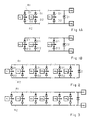
- FIG. 1A which corresponds to the state of the art described in EP-A-0 148 577, represents a conventional diagram of protection against electrostatic discharges of an integrated circuit comprising a single power source connected between a pad d VDD 1 high power supply and a VSS 1 low power supply pad.
- Each of the input / output pads P1 to Pn of the circuit is connected to a conductive rail R1 connected to the high supply pad VDD 1 via an isolation diode D1 whose anode is connected to the pad and the cathode to the rail R1.
- Each of the pads P1 to Pn is also connected to a rail R2 connected to the pad VSS 1 via an isolation diode D2 whose cathode is connected to the pad and the anode to the rail R2.
- Rail R1 is connected to rail R2 by a clipping device symbolized in the form of an avalanche diode Z1, the cathode of which is connected to rail R1 and the anode to rail R2.
- a clipping device symbolized in the form of an avalanche diode Z1, the cathode of which is connected to rail R1 and the anode to rail R2.
- Any conventional unidirectional clipping system can be used as the Z1 clipping device.
- This clipper has an avalanche threshold voltage greater than VDD 1 -VSS 1 but of course less than the value of the overvoltage against which the elements of the integrated circuit are to be protected.
- the diodes D1, D2 and the clipper Z1 are made inside of the integrated circuit and the rails R1 and R2 are metallizations formed on this integrated circuit. Note that the elements corresponding to diodes D1 and D2 are relatively weak surface but that, on the other hand, the realization of the Z1 clipper requires the occupation of a relatively large area of the integrated circuit.
- the circuit of FIG. 1A gives satisfaction as to protection against electrostatic discharge when the integrated circuit has a single power source external.
- this circuit has a drawback during the operation of the integrated circuit, namely that since each of the pads is connected to the high supply voltage by a direct diode and to the low supply voltage by a reverse diode, each of the studs cannot go up to more than 0.6 volt above the high voltage or go down to more than -0.6 volt below the low voltage VSS (commonly ground).
- VSS commonly ground
- output amplifiers can be connected to inductive loads; if overvoltages occur, they will be clipped by the connection to the upper power terminal, which may not be desirable.
- Modern integrated circuits often include several power sources (up to 7 for certain circuits). Each of these power sources includes a high power supply terminal VDDi and a low power supply terminal VSS i .
- the circuit of FIG. 1A has simply been extended by duplicating it by circuits such as that of FIG. 1B, as described for example US-A-5,034 845.
- the pads P1 to Pn being part of circuit portions connected to a first power source VDD 1 -VSS 1 , are connected by the circuit of FIG. 1A; and the pads P n + 1 to P n + k , being part of circuit portions connected to a second supply source VDD 2 -VSS 2 , are connected by a circuit similar to that of FIG. 1A, illustrated in FIG. 1B .
- This type of circuit is repeated as many times as there are power sources.
- a first drawback is that this structure requires as many Zi clippers as there are power sources. As noted earlier, these clippers occupy a relatively large area of the integrated circuit and this is contradictory with the desire to reduce surface area which is essential to any designer of integrated circuit.
- a second even more significant drawback of the simultaneous use of circuits such as those of FIGS. 1A and 1B in the same integrated circuit is that this type of protection is ineffective when an electrostatic discharge is caused between a pad P1 to Pn associated with a first power source and a pad P n + 1 to P n + k associated with a second power source. There is then no longer a path passing through a clipper to short-circuit the overload. This then propagates inside the integrated circuit and can have a destructive effect.
- an object of the present invention is to provide for an integrated circuit with several power supplies, a protective structure against electrostatic discharges between studs or pins which is perfectly effective while this integrated circuit is not connected.
- Another object of the present invention is to provide such a protective structure which further allows pads to mount at a voltage higher than the supply voltage the highest or go down to a voltage below the lowest supply voltage.
- Another object of the present invention is to provide such a protective structure which occupies a surface scaled down.
- the present invention provides a protection circuit according to claim 1. Specific embodiments of the present invention are described in the dependent claims.
- FIG. 2 schematically represents a circuit for protection against electrostatic overloads according to the present invention of an integrated circuit associated with several power supplies. These supplies are each applied between high VDD 1 , VDD 2 ... and low VSS 1 , VSS 2 ... supply terminals.
- the integrated circuit also includes conventional input / output pads P1, P2 ...
- the protection circuit according to the present invention comprises, as previously, rails R1 and R2 respectively connected to the cathode and to the anode of a clipper Z. As previously, each of the pads P1, P2 ... is connected to the rail R1 by a diode D1 polarized in direct and to the rail R2 by a diode D2 polarized in reverse.
- each of the high and low power supply pads VDD 1 , VDD 2 ..., VSS 1 , VSS 2 ... is also connected to these rails R1 and R2 by diodes D1 and D2 respectively forward and reverse polarized.
- the rails R1 and R2 are kept floating.
- any discharge between any one of the pads P1, P2 ..., and any other of these pads or any of the supply pads high or low will go through a diode D1, the clipping device Z and a diode D2.
- This type of protection therefore provides protection complete against electrostatic discharges between two pads any of the integrated circuit.
- An advantage of the protective structure according to the present invention is that it comprises a single Z clipper which whatever the number of power supplies in the circuit. This results in a surface reduction.
- one any of the pads P1, P2 ... may, during the operation of the integrated circuit, switch to a higher voltage than that of the upper or lower supply terminal higher or lower than that lowest power supply terminal. Indeed, the difference in voltage between two pads is always limited by the clipping voltage of the Z clipper (plus two direct voltage drops from diodes).
- FIG. 3 illustrates an alternative embodiment of the present invention in which there is substantially the same structure as that of FIG. 2 but in which the stud to be connected to the high voltage of highest value VDD i is connected to the rail R1 and the pad to be connected to the low voltage with the lowest value VSS j is connected to the rail R2.
- This variant also provides protection against all overvoltage configurations. It allows compared to the previous embodiment to save four isolation diodes which would be associated in the embodiment of Figure 2 with the pads VDD i and VSS j . However, it has the disadvantage of no longer allowing one of the pads P1, P2 ... to rise significantly above the highest voltage or to descend significantly below the lowest voltage.
- Figure 4 is a very schematic top view a portion of an integrated circuit where we have represented pads P1 to P8 which can also be input pads / output only supply pads. Typically, these pads are arranged on the periphery of the integrated circuit. Preferably, the rails R1 and R2 are also arranged at the periphery of the integrated circuit chip, in the vicinity of the pads, respectively below and beyond these compared to the center of the chip. The studs will be connected to these rails by the diodes integrated into the circuit in a conventional manner.
- each of high power pads can be connected to the rail connected to the cathode of the protection device via a pair of anti-parallel diodes and each of the power supply pads bass can be connected to the rail connected to the anode of the clipper also through a pair of diodes in anti-parallel.
Landscapes
- Semiconductor Integrated Circuits (AREA)
- Emergency Protection Circuit Devices (AREA)
- Protection Of Static Devices (AREA)
Description
Claims (4)
- Circuit de protection contre des surtensions électrostatiques des plots de connexion d'un circuit intégré à alimentations multiples, chaque alimentation étant connectée entre un plot de connexion à potentiel haut et un plot de connexion à potentiel bas, le circuit de protection comprenant :le circuit de protection étant de plus tel que :une pluralité de plots de connexion d'un circuit intégré à alimentations multiples se répartissant en une pluralité de plots d'entrée/sortie (P1, P2 ...), et en une pluralité de plots d'alimentation consistant en une pluralité de plots de connexion à potentiel haut (VDD1, VDD2..., .., VDDi, ...) et une pluralité de plots de connexion à potentiel bas (VSS1, VSS2, ..., VSSj, ...),une pluralité de premières diodes (D1),une pluralité de deuxièmes diodes (D2),un composant écrêteur unidirectionnel (Z),un premier rail conducteur (R1),un deuxième rail conducteur (R2) ;dans l'ensemble formé par tous les plots d'entrée-sortie (P1, P2, ...) et certains des plots d'alimentation (VDD1, VDD2, ..., VSS1, VSS2, ..., chaque plot est connecté à l'anode d'une des premières diodes (D1) dont la cathode est reliée au premier rail conducteur (R1) et à la cathode d'une des deuxièmes diodes (D2) dont l'anode est reliée au deuxième rail conducteur (R2), etle composant écrêteur unidirectionnel (Z) est connecté par sa cathode au premier rail conducteur (R1) et par son anode au deuxième rail (R2).
- Circuit de protection selon la revendication 1, caractérisé en ce que tous les plots d'alimentation sont connectés aux premières et deuxièmes diodes de la façon indiquée en revendication 1 pour lesdits certains des plots d'alimentation.
- Circuit de protection selon la revendication 1, caractérisé en ce que le plot (VDDi) au potentiel haut de l'alimentation la plus positive est connecté au premier rail et le plot (VSSj) à potentiel bas de l'alimentation la plus négative est connecté au deuxième rail.
- Circuit de protection selon la revendication 1, caractérisé en ce que les rails (R1, R2) sont constitués de pistes conductrices formées à la périphérie du circuit intégré, respectivement en-deçà et au-delà des plots de connexion.
Applications Claiming Priority (2)
| Application Number | Priority Date | Filing Date | Title |
|---|---|---|---|
| FR9309928 | 1993-08-06 | ||
| FR9309928A FR2708788B1 (fr) | 1993-08-06 | 1993-08-06 | Protection d'un circuit intégré à l'encontre de surcharges électrostatiques. |
Publications (2)
| Publication Number | Publication Date |
|---|---|
| EP0637843A1 EP0637843A1 (fr) | 1995-02-08 |
| EP0637843B1 true EP0637843B1 (fr) | 1999-10-13 |
Family
ID=9450167
Family Applications (1)
| Application Number | Title | Priority Date | Filing Date |
|---|---|---|---|
| EP94410062A Expired - Lifetime EP0637843B1 (fr) | 1993-08-06 | 1994-08-03 | Circuit de protection contre des surtensions |
Country Status (5)
| Country | Link |
|---|---|
| US (1) | US5515225A (fr) |
| EP (1) | EP0637843B1 (fr) |
| JP (1) | JPH07170655A (fr) |
| DE (1) | DE69421134T2 (fr) |
| FR (1) | FR2708788B1 (fr) |
Families Citing this family (19)
| Publication number | Priority date | Publication date | Assignee | Title |
|---|---|---|---|---|
| FR2685817B1 (fr) | 1991-12-31 | 1994-03-11 | Sgs Thomson Microelectronics Sa | Protection generale d'un circuit integre contre les surcharges permanentes et decharges electrostatiques. |
| US5675809A (en) * | 1995-02-10 | 1997-10-07 | Ncr Corporation | Voltage control circuit for a dual voltage bus computer system |
| US5708550A (en) * | 1995-10-25 | 1998-01-13 | David Sarnoff Research Center, Inc. | ESD protection for overvoltage friendly input/output circuits |
| US5715127A (en) * | 1996-05-06 | 1998-02-03 | Winbond Electronics Corp. | Method for preventing electrostatic discharge failure in an integrated circuit package |
| US5712753A (en) * | 1996-05-06 | 1998-01-27 | Winbond Electronics Corp. | Method for preventing electrostatic discharge failure in an integrated circuit package |
| JP3144308B2 (ja) | 1996-08-01 | 2001-03-12 | 日本電気株式会社 | 半導体装置 |
| US5740000A (en) * | 1996-09-30 | 1998-04-14 | Hewlett-Packard Co. | ESD protection system for an integrated circuit with multiple power supply networks |
| US5708549A (en) * | 1996-10-04 | 1998-01-13 | Harris Corporation | Integrated circuit having enhanced transient voltage protection and associated methods |
| DE19709716A1 (de) * | 1997-03-10 | 1998-05-14 | Siemens Ag | Ansteuerschaltung für wenigstens ein kapazitives Stellglied |
| GB2334633B (en) * | 1998-02-21 | 2002-09-25 | Mitel Corp | Low leakage electrostatic discharge protection system |
| US6977420B2 (en) | 1998-09-30 | 2005-12-20 | National Semiconductor Corporation | ESD protection circuit utilizing floating lateral clamp diodes |
| US6118640A (en) * | 1999-02-17 | 2000-09-12 | Pericom Semiconductor Corp. | Actively-driven thin-oxide MOS transistor shunt for ESD protection of multiple independent supply busses in a mixed-signal chip |
| US6421215B1 (en) * | 1999-10-08 | 2002-07-16 | Sun Microsystems, Inc. | Power overload protection for a system unit |
| US6456472B1 (en) * | 2000-04-07 | 2002-09-24 | Philsar Semiconductor Inc. | ESD protection in mixed signal ICs |
| US6580591B2 (en) * | 2000-12-21 | 2003-06-17 | Intersil Americas, Inc. | Switched electrostatic discharge ring for integrated circuits with multiple power inputs |
| US6801416B2 (en) | 2001-08-23 | 2004-10-05 | Institute Of Microelectronics | ESD protection system for high frequency applications |
| US7362555B2 (en) * | 2006-08-26 | 2008-04-22 | Taiwan Semiconductor Manufacturing Co., Ltd. | ESD protection circuit for a mixed-voltage semiconductor device |
| US8018002B2 (en) | 2009-06-24 | 2011-09-13 | Globalfoundries Inc. | Field effect resistor for ESD protection |
| JP5719126B2 (ja) * | 2010-06-16 | 2015-05-13 | ルネサスエレクトロニクス株式会社 | 内部回路と静電保護回路を具備する半導体集積回路 |
Family Cites Families (6)
| Publication number | Priority date | Publication date | Assignee | Title |
|---|---|---|---|---|
| JPS59191371A (ja) * | 1983-04-14 | 1984-10-30 | Nec Corp | 相補型mos電界効果装置 |
| EP0148577A1 (fr) * | 1983-11-14 | 1985-07-17 | General Semiconductor Industries Inc. | Protection de surtension |
| US4819047A (en) * | 1987-05-15 | 1989-04-04 | Advanced Micro Devices, Inc. | Protection system for CMOS integrated circuits |
| US4996626A (en) * | 1988-10-14 | 1991-02-26 | National Semiconductor Corp. | Resistorless electrostatic discharge protection device for high speed integrated circuits |
| JPH02113623A (ja) * | 1988-10-21 | 1990-04-25 | Sharp Corp | 集積回路の静電気保護回路 |
| EP0435047A3 (en) * | 1989-12-19 | 1992-07-15 | National Semiconductor Corporation | Electrostatic discharge protection for integrated circuits |
-
1993
- 1993-08-06 FR FR9309928A patent/FR2708788B1/fr not_active Expired - Fee Related
-
1994
- 1994-08-03 EP EP94410062A patent/EP0637843B1/fr not_active Expired - Lifetime
- 1994-08-03 DE DE69421134T patent/DE69421134T2/de not_active Expired - Fee Related
- 1994-08-04 JP JP6201559A patent/JPH07170655A/ja active Pending
- 1994-08-04 US US08/286,490 patent/US5515225A/en not_active Expired - Lifetime
Also Published As
| Publication number | Publication date |
|---|---|
| FR2708788A1 (fr) | 1995-02-10 |
| US5515225A (en) | 1996-05-07 |
| DE69421134D1 (de) | 1999-11-18 |
| DE69421134T2 (de) | 2000-02-03 |
| FR2708788B1 (fr) | 1995-10-27 |
| EP0637843A1 (fr) | 1995-02-08 |
| JPH07170655A (ja) | 1995-07-04 |
Similar Documents
| Publication | Publication Date | Title |
|---|---|---|
| EP0637843A1 (fr) | Protection d'un circuit intégré à l'encontre de surcharges électrostatiques | |
| EP0576375B1 (fr) | Structure de diodes de protection de plot | |
| KR100200057B1 (ko) | 집적 회로용 정전방전 보호회로 | |
| US7920366B2 (en) | ESD configuration for low parasitic capacitance I/O | |
| EP0562982B1 (fr) | Circuit intégré constituant un réseau de diodes de protection | |
| EP0551038A1 (fr) | Protection générale d'un circuit intégré contre les surcharges permanentes et décharges électrostatiques | |
| WO2017203187A1 (fr) | Circuit intégré comprenant une pluralité de puces formées d'un transistor à haute tension et comprenant une puce formée d'un transistor à basse tension | |
| US5805009A (en) | Method for operating an electrostatic discharge protection circuit | |
| EP0543745B1 (fr) | Transistor MOS à zener de protection intégrée | |
| FR2670340A1 (fr) | Circuit de protection a faible capacite. | |
| FR2775392A1 (fr) | Systeme de protection vis-a-vis d'une decharge electrostatique a fuite faible | |
| FR2713400A1 (fr) | Composant de protection triangle. | |
| US20020093775A1 (en) | Esd protection in mixed signal ics | |
| EP0738038B1 (fr) | Amplificateur de courant | |
| EP0619637B1 (fr) | Protection d'un alternateur triphasé automobile | |
| EP4037125A1 (fr) | Dispositif de protection contre les décharges électrostatiques | |
| JP2870514B2 (ja) | 半導体装置 | |
| EP0450245A2 (fr) | Détecteur de variation rapide d'alimentation de circuit intégré | |
| EP1309005B1 (fr) | Protection d'un circuit intégré contre des décharges électrostatiques et autres surtensions | |
| EP2246886A1 (fr) | Circuit intégré muni d'une protection de grande surface contre les décharges électrostatiques | |
| EP0895331B1 (fr) | Dispositif de protection d'une charge électrique et circuit d'alimentation comportant un tel dispositif | |
| EP0881681B1 (fr) | Composant de protection d'un transitor MOS intégré contre des gradients de tension | |
| FR2664759A1 (fr) | Dispositif de protection contre des surtensions. | |
| JPH03503944A (ja) | 静電放電現象によるjfetの損傷を減少するための手段 | |
| EP0554195A1 (fr) | Composant de protection semiconducteur auto-protégé |
Legal Events
| Date | Code | Title | Description |
|---|---|---|---|
| PUAI | Public reference made under article 153(3) epc to a published international application that has entered the european phase |
Free format text: ORIGINAL CODE: 0009012 |
|
| AK | Designated contracting states |
Kind code of ref document: A1 Designated state(s): DE FR GB IT |
|
| 17P | Request for examination filed |
Effective date: 19950717 |
|
| 17Q | First examination report despatched |
Effective date: 19970923 |
|
| GRAG | Despatch of communication of intention to grant |
Free format text: ORIGINAL CODE: EPIDOS AGRA |
|
| RAP3 | Party data changed (applicant data changed or rights of an application transferred) |
Owner name: STMICROELECTRONICS S.A. |
|
| GRAG | Despatch of communication of intention to grant |
Free format text: ORIGINAL CODE: EPIDOS AGRA |
|
| GRAH | Despatch of communication of intention to grant a patent |
Free format text: ORIGINAL CODE: EPIDOS IGRA |
|
| GRAH | Despatch of communication of intention to grant a patent |
Free format text: ORIGINAL CODE: EPIDOS IGRA |
|
| GRAA | (expected) grant |
Free format text: ORIGINAL CODE: 0009210 |
|
| AK | Designated contracting states |
Kind code of ref document: B1 Designated state(s): DE FR GB IT |
|
| REF | Corresponds to: |
Ref document number: 69421134 Country of ref document: DE Date of ref document: 19991118 |
|
| GBT | Gb: translation of ep patent filed (gb section 77(6)(a)/1977) |
Effective date: 19991111 |
|
| ITF | It: translation for a ep patent filed | ||
| PLBE | No opposition filed within time limit |
Free format text: ORIGINAL CODE: 0009261 |
|
| STAA | Information on the status of an ep patent application or granted ep patent |
Free format text: STATUS: NO OPPOSITION FILED WITHIN TIME LIMIT |
|
| 26N | No opposition filed | ||
| REG | Reference to a national code |
Ref country code: GB Ref legal event code: IF02 |
|
| PGFP | Annual fee paid to national office [announced via postgrant information from national office to epo] |
Ref country code: DE Payment date: 20030814 Year of fee payment: 10 |
|
| PG25 | Lapsed in a contracting state [announced via postgrant information from national office to epo] |
Ref country code: DE Free format text: LAPSE BECAUSE OF NON-PAYMENT OF DUE FEES Effective date: 20050301 |
|
| PG25 | Lapsed in a contracting state [announced via postgrant information from national office to epo] |
Ref country code: IT Free format text: LAPSE BECAUSE OF NON-PAYMENT OF DUE FEES;WARNING: LAPSES OF ITALIAN PATENTS WITH EFFECTIVE DATE BEFORE 2007 MAY HAVE OCCURRED AT ANY TIME BEFORE 2007. THE CORRECT EFFECTIVE DATE MAY BE DIFFERENT FROM THE ONE RECORDED. Effective date: 20050803 |
|
| PGFP | Annual fee paid to national office [announced via postgrant information from national office to epo] |
Ref country code: GB Payment date: 20060802 Year of fee payment: 13 |
|
| PGFP | Annual fee paid to national office [announced via postgrant information from national office to epo] |
Ref country code: FR Payment date: 20060808 Year of fee payment: 13 |
|
| GBPC | Gb: european patent ceased through non-payment of renewal fee |
Effective date: 20070803 |
|
| REG | Reference to a national code |
Ref country code: FR Ref legal event code: ST Effective date: 20080430 |
|
| PG25 | Lapsed in a contracting state [announced via postgrant information from national office to epo] |
Ref country code: FR Free format text: LAPSE BECAUSE OF NON-PAYMENT OF DUE FEES Effective date: 20070831 |
|
| PG25 | Lapsed in a contracting state [announced via postgrant information from national office to epo] |
Ref country code: GB Free format text: LAPSE BECAUSE OF NON-PAYMENT OF DUE FEES Effective date: 20070803 |