EP0637186B1 - Systèmes et multiplexeurs pour l'allocation d'intervalle de temps - Google Patents
Systèmes et multiplexeurs pour l'allocation d'intervalle de temps Download PDFInfo
- Publication number
- EP0637186B1 EP0637186B1 EP94460022A EP94460022A EP0637186B1 EP 0637186 B1 EP0637186 B1 EP 0637186B1 EP 94460022 A EP94460022 A EP 94460022A EP 94460022 A EP94460022 A EP 94460022A EP 0637186 B1 EP0637186 B1 EP 0637186B1
- Authority
- EP
- European Patent Office
- Prior art keywords
- input
- time interval
- output
- circuit
- cell
- Prior art date
- Legal status (The legal status is an assumption and is not a legal conclusion. Google has not performed a legal analysis and makes no representation as to the accuracy of the status listed.)
- Expired - Lifetime
Links
Images



Classifications
-
- H—ELECTRICITY
- H04—ELECTRIC COMMUNICATION TECHNIQUE
- H04J—MULTIPLEX COMMUNICATION
- H04J3/00—Time-division multiplex systems
- H04J3/24—Time-division multiplex systems in which the allocation is indicated by an address the different channels being transmitted sequentially
- H04J3/247—ATM or packet multiplexing
-
- H—ELECTRICITY
- H04—ELECTRIC COMMUNICATION TECHNIQUE
- H04Q—SELECTING
- H04Q11/00—Selecting arrangements for multiplex systems
- H04Q11/04—Selecting arrangements for multiplex systems for time-division multiplexing
- H04Q11/0428—Integrated services digital network, i.e. systems for transmission of different types of digitised signals, e.g. speech, data, telecentral, television signals
- H04Q11/0478—Provisions for broadband connections
-
- H—ELECTRICITY
- H04—ELECTRIC COMMUNICATION TECHNIQUE
- H04L—TRANSMISSION OF DIGITAL INFORMATION, e.g. TELEGRAPHIC COMMUNICATION
- H04L12/00—Data switching networks
- H04L12/54—Store-and-forward switching systems
- H04L12/56—Packet switching systems
- H04L12/5601—Transfer mode dependent, e.g. ATM
- H04L2012/5603—Access techniques
- H04L2012/5609—Topology
- H04L2012/5612—Ring
-
- H—ELECTRICITY
- H04—ELECTRIC COMMUNICATION TECHNIQUE
- H04L—TRANSMISSION OF DIGITAL INFORMATION, e.g. TELEGRAPHIC COMMUNICATION
- H04L12/00—Data switching networks
- H04L12/54—Store-and-forward switching systems
- H04L12/56—Packet switching systems
- H04L12/5601—Transfer mode dependent, e.g. ATM
- H04L2012/5614—User Network Interface
- H04L2012/5616—Terminal equipment, e.g. codecs, synch.
-
- H—ELECTRICITY
- H04—ELECTRIC COMMUNICATION TECHNIQUE
- H04L—TRANSMISSION OF DIGITAL INFORMATION, e.g. TELEGRAPHIC COMMUNICATION
- H04L12/00—Data switching networks
- H04L12/54—Store-and-forward switching systems
- H04L12/56—Packet switching systems
- H04L12/5601—Transfer mode dependent, e.g. ATM
- H04L2012/5672—Multiplexing, e.g. coding, scrambling
Definitions
- the present invention relates to allocation systems time interval and multiplexers with one of these time interval allocation systems.
- Each cell in the system of transmission is associated with a virtual communication circuit.
- Each cell consists, on the one hand, of a so-called header part in which information relating to systems is stored, in particular the number of the virtual circuit to which it belongs and, on the other hand, from a part where messages are present to transmit.
- n can be equal to eight for a global switched speed of around 155 Mbits / s.
- access to the bus poses allocation problems time interval in order to avoid in particular the collision of cells or the overflow of the output queues.
- the object of the invention is to propose allocation systems time interval that can solve the problems mentioned above when these systems are applied to multiplexers. These systems are not limited to these particular applications.
- Another object of the invention is also to propose multiplexers with n inputs and one output which make it possible to solve the problems of access to the bus.
- Another object of the invention is also to propose multiplexers which also make it possible to integrate means of control and spacing of emissions from cells belonging to the same virtual circuit.
- a time slot allocation system is characterized in that it includes a time interval management unit delivering, at each time interval, the last interval of time that has been allocated and a plurality of counters linked together in series so that the input of a counter is connected to the exit of the previous counter in the series, entry of the first counter being connected to the output of the interval management unit of time, each counter being associated with an entry carrying a time slot allocation request signal and being provided a control input intended to receive said request signal allocation and delivering either the time interval value present on its input if said allocation request signal is inactive, i.e.
- each counter being connected to the input of a register of which the control input is provided to receive said request signal corresponding, each register then delivering, if said signal corresponding request is active, a time interval signal allocated.
- the present invention relates to a time slot allocation system intended to allocate a time interval to a cell of a communication system present on the input of an input circuit of a multiplexer, said multiplexer comprising several input circuits grouped together as a group forming a plurality of input circuit groups.
- This system is then characterized in that it comprises a time interval management unit delivering, at each time interval, the last time slot that was allocated, said groups of input circuits being connected together in series so that the input of a group is connected to the output of the previous group in the series, the input of the first group being linked to the output of the time interval management unit, each group comprising several adders respectively associated with allocation request signals time interval emanating respectively from said input circuits of said group corresponding, said adders having a first input connected to the input of said group, each row adder (j) having its second input connected to the calculation to receive a signal representative of the number of demand signals active allocation present on inputs associated with adders of the same group but of lower rank as well as on the entry with which it is associated, and its output which is connected to the input of a register whose command input is intended for receive said associated allocation request signal, each register then delivering, if said corresponding request signal is active, a time interval signal which is allocated to the cell which is present on the input of the corresponding input circuit, the output of
- the unit of time interval management receives time interval value which is present on the output of the last counter or the last group and delivers it to the first counter or first group as as the value of the last allocated time interval.
- the time interval management unit when the difference between the time interval value of the signal received by the time interval management unit and the interval value of current time is zero, the time interval management unit delivers a signal whose value corresponds to the value of the current time interval plus one.
- each counter is provided so that when the difference between the value of time interval of the signal present on its input and the value of the current time interval exceeds a threshold value predetermined, it no longer increments the time interval value on its entry, even if a cell is present on the entry corresponding.
- the invention therefore also relates to a multiplexer of the type which comprises n inputs intended to receive communication cells in cell time intervals and an output intended to supply, during a determined cell time interval, one of said cells.
- a counter or an adder and a calculation circuit, the cell memory partner, the associated register and the associated request means together form a single circuit called the input circuit.
- a memory of cell and the associated register together form a single circuit called input circuit, the adders and the calculation circuit of a group being brought together to form a single control circuit for group.
- said means request used to generate an allocation request signal assets consist of a translation memory whose entry addressing address is intended to receive the circuit number virtual of a cell on the corresponding input.
- the invention also relates to a multiplexer which is also of the type allowing the emission of cells belonging to the same virtual circuit at substantially regular time intervals temporally spaced.
- each unit of determination of the estimated cell emission time is made up a translation memory, each of the boxes of which is addressed in read by the virtual circuit number to which the cell belongs present on the corresponding entry, each box of said memory with a field in which a period is stored assigned to said corresponding virtual circuit and a field containing the theoretical emission time of the last emitted cell belonging to said virtual circuit, the read outputs of said memory corresponding respectively to said fields being respectively connected to the inputs of a calculation unit intended to deliver on its output of said theoretical transmission time signal or estimated time to send it to the write addressing input of said corresponding address memory, said signal also being supplied to the write input of the translation memory for its writing in the corresponding field.
- it comprises in addition to an address availability circuit which, depending on the availability of the address memory box sent by the theoretical transmission time signal, determines a time signal estimated emission.
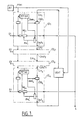
- the multiplexer shown in FIG. 1 includes four inputs E 1 to E 4 and an output S.
- the inputs E 1 to E 4 are respectively connected to the inputs of input circuits CE 1 to CE 4 , the outputs of which are connected to the output S.
- It also includes a UGIT time interval management unit designed to deliver, at each time interval, a signal representative of the last interval that has been allocated. It also comprises a time base BT whose output which delivers a local time signal Hloc is connected to each of the corresponding inputs of the input circuits CE 1 to CE 4 and also to an input of the unit UGIT.
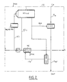
- FIG. 2 There is shown in FIG. 2 the block diagram of a circuit CE entry.
- the CE circuit shown essentially comprises a multi-wire input E, a RegAdMtr register, a memory of Mtrad translation, MC cell memory, delay circuit RET, a RegAd register and a CSO counter.
- the Mtrad memory is a memory of the random access memory type, the storage boxes of which are respectively associated with the virtual circuits which the system can process. In each of its boxes, are stored, at the initialization of the system, the virtual circuit number VCI t corresponding to the virtual circuit associated with said box as well as a dem bit, said subsequently allocation allocation bit time interval.
- the memory MC is a memory comprising a certain number of boxes each of which is designed to store a cell.
- the wires which carry the virtual circuit number VCI to which the cell present on the input E belongs are connected to the input of the register RegAdMtr, the output of which is linked to the address for read address of the translation memory Mtrad. In reading, the latter delivers a translated virtual circuit number VCI t which is then supplied to the input of the memory MC, as well as said allocation request bit dem.
- the other wires are connected, via a RET delay circuit, to the MC memory entry.
- the RET delay circuit is provided for compensate for the time delays introduced by the Mtrad memory.
- MC memory has its reading output which is connected to the output S of the CE circuit.
- Each cell of the MC memory is read by the local time signal Hloc delivered by the time base BT of the multiplexer and is addressed in writing by the interval signal ITa time allocation issued by the RegAd register.
- the CSO counter has its input which is connected to the so-called input time interval Cin of the input circuit CE and its output which is connected to the Cout time interval output of the CE circuit. he further includes a control input which is connected to an output of Mtrad memory to receive the allocation request signal dem.
- the CSO counter receives on its input an interval value of ITin time present on the Cin input of the CE input circuit. If the dem allocation request signal on its command input is not active, this time interval value is delivered on its output and therefore on the time interval output Cout of the circuit CE entry. However, if the dem allocation request signal is active, i.e. when a cell is present on input E of the input circuit CE, the time interval value ITin on the CSO counter input is incremented by one and the value incremented is delivered on its output and therefore on the Cout output of the CE input circuit.
- the RegAd register has its input which is connected to the output of the CSO counter. It has a control input which is connected to the output of the Mtrad memory which carries the request for allocation request request.
- the dem allocation request signal When the dem allocation request signal is active, the value ITout time interval present on the RegAd registry entry is transferred to its output and forms the time interval signal allocated ITa.
- the dem signal When the dem signal is not active, the value ITa on the output of the RegAd register is not modified whatever the time interval value ITout present on its input.
- Fig. 1 the time interval output Cout n of the input circuit CE n of rank n is connected to the time interval input Cin n + 1 of the input circuit CE n + 1 of rank n + 1 It can also be seen that the time interval input of the first input circuit CE 1 is connected to the output of the unit UGIT and that the input of the latter is connected to the time interval output Cout 4 of the last CE input circuit 4 .
- the multiplexer shown in FIG. 1 comprises four inputs E 1 to E 4 and an output S but the invention also relates to multiplexers with n inputs and an output S.
- the time interval management unit UGIT Upon initialization of the multiplexer, the time interval management unit UGIT delivers on its output a signal whose time interval value is equal to the current time interval Hloc plus one. This value is supplied on the Cin 1 input of the first CE 1 input circuit.
- the time interval value which is present on the Cin 1 input is found on the Cout 1 output and, consequently, on the Cin 2 input of the CE 2 input circuit.
- the absence of cells on the input E 1 implies that the allocation request signal dem 1 which is delivered by the memory Mtrad 1 on the control input of the counter CSO 1 is not active.
- the account value present on the input Cin 2 of the input circuit CE 2 is found on the output Cout 2 and therefore on the input Cin 3 of the input circuit CE 3 . If no cell is present on any of the inputs of circuits CE 1 to CE 4 , the time interval value at the output of the last input circuit CE 4 is found on the input of the management unit UGIT.
- the management unit UGIT is provided so that when the difference between the time interval value of the signal on the output of the last counter CSO 4 and the value of the current time interval Hloc as delivered by the time base BT is zero, it delivers, on its output and therefore on the input Cin 1 of the first input circuit CE 1 , a time interval signal whose value corresponds to the value of the interval of current time Hloc plus one.
- each counter CSO i is provided so that, when the difference between the time interval value of the signal IT in present on its input and the value of the current time interval Hloc exceeds a predetermined threshold value, it no longer increments the time interval value IT in on its input, even if a cell is present on the corresponding input E i .
- a cell is present on an input Ei of an input circuit CEi, its header, containing the number of VCI to which it belongs, is supplied, via the register RegAdMtr, to the addressing input of the Mtrad memory.
- the latter then delivers, on the one hand, a header containing the translated VCI number t and, on the other hand, the allocation request signal dem i .
- the information part of the cell as well as its translated header VCI t are then present on the write input of the cell memory MC i .
- the request signal dem i is supplied to the command input of the counter CSO i as well as to the command input of the register RegAd i .
- the counter CSO i increments the time interval value which is present on its input Cin i by one and delivers the incremented value on its output as the new allocated time interval value.
- This new time interval value can be found on the entry of the RegAd register and also on its exit. She addresses write MC memory.
- the cell on the input of the memory MC is therefore stored at the address whose value is equal to the new interval value ITa time.
- each time interval value flowing from input circuit to input circuit represents the value of the last time interval that was allocated for the emission of a cell.
- the MC memory is read in by the time signal local Hloc delivered by the BT time base.
- the cell which is stored at the address corresponding to the value of this Hloc signal is thus delivered on the output of the memory MC and is found on the output S of the multiplexer.
- each CSO counter must present a propagation time of the time interval value not negligible compared to the elementary duration of an interval of time.
- each time interval delivered by the time base BT is subdivided into a number of micro intervals t 1 to t m and one of these micro time intervals is assigned to each input circuit THIS i .
- Unassigned time slots are supported by the UGIT unit.
- all of the input circuits CE 1 to CE 4 operate in a strictly synchronous manner.
- the CSO counters of these input circuits are no longer linked to the BT time base.
- the propagation time of the account value from one input circuit to the next is equal not to a division of the duration of a time interval but to the propagation time in the CSO counter of an input circuit CE .
- each CSO counter can then be replaced by an adder which adds one to the time interval value ITin present on its input only if the request signal allocation allowance is active.
- the Mtrad memory of each input circuit constitutes a means to generate a dem request signal when a cell is present on a corresponding input E of the multiplexer.
- FIG. 3 There is shown in FIG. 3 a GRCE group of four input circuits CE 1 to CE 2 connected to a CGG group management circuit. As will be understood below, such a group of input circuits makes it possible to increase the number of inputs E i processed without increasing the processing speed.
- the input circuit CE 1 is shown with its cell memory MC, its means for generating a time slot allocation request GD and its register RegAd.
- the means GD deliver the request signal dem 1 which is supplied to an input of the management circuit CGG
- the output of the memory MC is connected to the output S of the group GRCE
- the input of the register RegAd is connected to an output Cost 1 of the CGG management circuit.
- the other input circuits CE 2 to CE 4 constituted and connected in a completely similar way to the input circuit CE 1 .
- the group management circuit CGG has an input which is connected to the input Cin of the group GRCE to receive there the value of the last allocated time interval ITin.
- the GRCE group Cout time interval output consists of the signal delivered by the CGG group management circuit on its Cout 4 output.
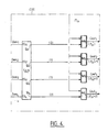
- FIG. 4 There is shown in FIG. 4 a CGG management circuit. It consists of a Som calculation circuit which is provided with four inputs ES 1 to ES 4 which receive the allocation request signals dem 1 to dem 4 generated by the input circuits CE 1 to CE 4 of the GRCE group. (Fig. 3). It has four outputs SS 1 to SS 4 , the first of which carries the value 1 or 0 depending on whether the first request request signal dem 1 is active or not, the second of which carries the value of the number of request signals dem 1 and dem 2 active, the third of which carries the value of the number of signals dem 1 , dem 2 and dem 3 active and the fourth output of which carries the value of the number of signals dem 1 to dem 4 active.
- Each output SS i of the Som circuit is connected to a first input of an adder Add i , the second input of which is intended to receive the time interval value ITin present on the input Cin of the GRCE group.
- the output of each Add i adder constitutes the Cout i output of the CGG group management circuit.
- the operation of such a group of input circuits is as follows. For example, if cells E 2 and E 4 of the GRCE group are present respectively, the allocation request signals dem 2 and dem 4 are active. It follows that the first SS 1 output of the Som circuit of the CGG group management circuit carries the value 0, the second SS 2 carries the value 1, the third SS 3 also carries the value 1 and the last SS 4 carries the value 2.
- time interval values in this example are in parentheses in Fig. 4. Only the registers of the input circuits CE 2 and CE 4 will store the time interval values ITin + 1 and ITin + 2 present on their inputs. The others will not be changed. In addition, the value ITin + 2 is supplied to another group of four input circuits.
- a CE input circuit like the one shown in Fig. 5.
- Fig. 6 a group of four input circuits according to Fig. 5.
- the input circuit CE of FIG. 5 further comprises a summing circuit Somm with four inputs ES 1 to ES 4 intended to receive respectively allocation request signals Dem 1 to dem 4 as will be explained below in relation to FIG. 6.
- the summation circuit Somm delivers on its output a signal SS representative of the number of its inputs ES 1 to ES 4 which carry an active dem allocation request signal and supplies it to a first input of an addition circuit Add whose other input is intended to receive the time interval value ITin present on the input Cin of the input circuit CE.
- the output of the addition circuit Add constitutes the output Cout of the input circuit CE and the signal ITout which it carries is supplied to the input of the register RegAd.
- the dem allocation request signal is found on the output Cdem of the input circuit CE.
- the four input circuits CE 1 to CE 4 are interconnected as shown in FIG. 6.
- the input circuits CE 1 to CE 4 are represented by mixed dotted lines and by their circuits Somm 1 to Somm 4 and by their circuits Add 1 to Add 4 . It can be seen that the inputs ES 1 of the summing circuits Somm 1 to Somm 4 respectively receive the allocation request signals dem 1 to dem 4 .
- the three inputs ES 2 to ES 4 of the summing circuit Somm 1 of the first input circuit CE 1 are connected to zero, that the input ES 2 of the circuit Somm 2 of the input circuit CE 2 is connected at the output Cdem 1 of the first circuit CE 1 while the other inputs ES 3 and ES 4 of the circuit Somm 2 are connected to zero.
- the input ES 2 of the summing circuit Somm 3 of the third input circuit CE 3 is connected to the output Cdem 1 of the first circuit CE 1 , its input ES 3 is connected to the output Cdem 2 of the second circuit CE 2 while its input ES 4 is connected to zero.
- the input ES 2 of the summing circuit Somm 4 of the fourth input circuit CE 4 is connected to the output Cdem 1 of the first input circuit CE 1 , the input ES 3 to the output Cdem 2 of the second circuit CE 2 and the ES 4 input at the Cdem 3 output of the third circuit.
- the Cout 4 output of the fourth input circuit CE 4 constitutes the Cout time interval output of the GRCE group.
- the Cin input of all the input circuits CE 1 to CE 4 is connected to the interval input Cin of the GRCE group.
- the operation of such a GRCE group is as follows. Suppose, as in the previous example, that the inputs E 2 and E 4 of a group comprising the inputs E 1 to E 4 have made a request, that is to say that the allocation request signals dem 2 and dem 4 are active.
- the output of the first circuit Somm 1 carries the value 0 so that the value of IT 1 is equal to ITin on the input Cin of the GRCE group.
- the output Cdem 1 of the first input circuit CE 1 carries the value zero.
- the output of the second circuit Somm 2 carries the value one insofar as the request signal dem 2 is active.
- the value IT 2 is therefore equal to the value ITin + 1. Since the signal dem 2 is active, the cell present on the input E 2 is therefore stored in the memory MC of the input circuit CE 2 at the address corresponding to ITin + 1.
- the Cdem 2 value of the second CE 2 circuit is equal to one .
- the output of the third circuit Somm 3 carries the value one insofar as only the input ES 3 of the circuit Somm 3 carries the value one , the others being at zero.
- the value IT 3 is equal to the value ITin + 1 but it is not used in the input circuit CE 3 .
- the Cdem 3 output carries the value one .
- the output of the fourth circuit Somm 4 carries the value two insofar as the allocation request signal dem 4 is active and the input ES 3 of the circuit Somm 4 carries a value equal to one .
- the value IT 4 is equal to ITin + 2 and the cell on the input E4 is stored at the address of the memory MC of the input circuit CE 4 .
- the Cout 4 output therefore carries the value ITin + 2. This value corresponds, in the system, to the last IT time interval for which a cell transmission has been scheduled.
- FIG. 7 a time interval allocation system according to the invention. It comprises a time interval management unit UGIT and a plurality of counters CSO 1 to CSO n linked together in series so that the input of a counter CSO i is connected to the output of the previous counter CSO i - 1 in the series, so that the input of the first CSO counter 1 is connected to the output of the time interval management unit UGIT and that the output of the last CSO counter n is connected to an input of the UGIT unit.
- Each counter CSO i is associated with an input carrying an allocation request signal dem i and is provided with a control input provided for receiving said signal dem i .
- Each CSO counter i is designed to deliver either the time interval value present on its input if said corresponding allocation request signal dem i is inactive, or the time interval value present on its input incremented by a unit if said corresponding request signal dem i is active.
- the output of each counter CSO i is connected to the input of a register RegAd i whose command input is provided to receive said corresponding request signal dem i
- Each register RegAd i is designed to deliver, if said corresponding request signal dem i is active, an allocated time interval signal IT i .
- the operation of the UGIT unit is the same as that of the UGIT unit of the multiplexer of FIG. 1. The same applies to CSO counters.
- the multiplexer of FIG. 1 can be considered to be made up of a plurality of cell memories MC each associated with an input E i of the multiplexer, a plurality of request means Mtrad and a time slot allocation system such as that which is shown in Fig. 7.
- Each memory MC is addressed in writing by the time interval signal IT i delivered by the register RegAd i of the allocation system.
- the operation of the allocation system of FIG. 7 can therefore deduce from the operation of the multiplexer according to FIG. 1.
- the multiplexers of FIG. 3 and from Fig. 5 can be considered to be provided with means allocation of time intervals, of a plurality of memories of cell and a plurality of signal generation means allowance request.
- each input circuit CE i can be equipped with a device for temporally spacing two transmissions of cells belonging to the same virtual circuit such as one of the devices which are notably described in the patent documents FR- A-2 668 324 and FR-A-2 686 205.
- FIG. 8 there is shown an input circuit CE which is provided with means for spacing the cells present on its input E.
- the aim of such a system is the emission of cells belonging to a same virtual circuit at substantially time intervals regularly spaced in time, for example by a period T.
- This CE input circuit includes a CSO counter which has an input Cin and a Cout outlet.
- the CSO counter is controlled by a signal request for allocation of time interval present on its entry control. It also includes a RegAd register whose entry is connected to the output of the CSO counter and whose command input is scheduled to receive the request for allocation request request. he delivers on its output an allocated time interval signal ITa.
- the multiplexer according to FIG. 8 still has a memory of MCel cells whose writing input is connected, via a circuit delay R, at the input E of the input circuit CE. Leaving the memory MCel is connected to the output S of the CE circuit. MCel memory is planned to be able to store the cells which are present on input E of the CE circuit.
- each box of which is addressed by a VCI virtual circuit number contains, in addition to a circuit number virtual translates VCIt and a validation signal En, part, called of context, containing the theoretical time of Hted emission of the last cell sent having the associated VCI virtual circuit number to the cell as well as the time period T assigned to the cells which belong to this VCI virtual circuit.
- Cells that are stored in MCel memory are stored with their virtual circuit number translated VCIt as delivered by Mtrad memory.
- Time reading outputs from Mtrad memory theoretical Hted, period T and validation bit En are linked to the corresponding inputs of a VSA time calculation circuit theoretical Hte emission of the current cell present on the input E.
- the output of the VSA calculation circuit is connected to the input writing in the Hted field of the Mtrad memory. She is also connected to the input of an available address calculation circuit GDR whose output is connected to the write addressing input of a address memory MAd.
- the function of the GDR calculation circuit is to calculate the first unoccupied address of the memory MAd of value Hee corresponding to a estimated emission time, starting from the address which corresponds to the theoretical time Hte delivered by the VSA calculation circuit.
- Such circuit is for example constituted by the circuit described in the document FR-A-2 617 302 under the reference MAD.
- An available write address calculation circuit CAd has its output which is connected to the write addressing input of the MCel cell memory to deliver an available address Adre in order to memorize, at this address Adre, the current cell present on input E.
- the CAd circuit can consist of a counter whose the output increments by one each time a cell arrives on entrance E.
- the output of the CAd circuit is also connected to the input writing memory MAd. So the address Adre, that is to say the address where the current cell is stored is stored in the MAd memory at an address which corresponds to the estimated time of transmission Hee delivered by the GDR circuit.
- the addressing address for reading from the memory MAd is connected to the time base to receive the local time signal Hloc there.
- the memory read output MAd is connected to an input writing a transmission memory MEm whose reading output is connected to the addressing address in read memory MCel for y issue an Adrl reading address. While reading the MAd memory, its output delivers the allocation request signal time interval at the CSO counter command input.
- the memory MEm has its write addressing input which is linked to the output of the RegAd register.
- the memory MEm has its read addressing input which is connected to the BT time base to receive the local time signal there Hloc.
- the Hted time, the period T and the validation signal En are delivered to the VSA calculation circuit which delivers the theoretical time Hte transmission from the cell present on input E. This time is for example calculated by adding the Hted hour and the T period. It is issued to a write entry in the Mtrad memory for its storage in place of the Hted value.
- the high time is delivered to the GDR calculation circuit which delivers the estimated Hee emission time and provides it to the addressing input in writing of the memory MAd.
- the calculation circuit CAd delivers the address signal Adre corresponding to an unoccupied address in the MCel memory.
- This signal Adre is delivered to the write addressing address of the memory MCel so that it stores there the cell which is present on input E of the CE circuit.
- This address signal is also supplied to the write input of the memory MAd.
- the address at which is stored, in memory MCel, the cell on input E is therefore stored in MAd memory at an address that corresponds to the time Hee emission estimate calculated by the GDR circuit.
- a new value ITin time interval is found on entry Cin. She corresponds to the last cell time interval which has already been allocated.
- the memory MAd is read in by the local time signal Hloc delivered by the time base BT.
- the memory MAd then delivers an address signal Adr corresponding to the address in MCel memory of a cell whose emission time estimated is equal to local time Hloc. It also delivers a active dem allocation request signal which then controls the CSO counter. This therefore increments the interval value by ITin time which is on its Cin input and delivers this value incremented on the Cout output.
- the register RegAdr also delivers ITa allocated time interval signal on the write addressing input of the memory MEm.
- the value of address Adr delivered by the memory MAd is therefore stored in the memory MEm at an address which corresponds to the interval of ITa.
- the memory MEm is also addressed in reading by the local time signal Hloc delivered by the base of time.
- the memory MEm then delivers an address signal Adrl which is supplied to MCel memory.
- Adrl which is supplied to MCel memory.
- the cell stored at the address Adrl corresponding to this signal is then transmitted. We will understand that she is issued during the cell time allocated to it at the time of storage of its address in the memory MEm.
Landscapes
- Engineering & Computer Science (AREA)
- Computer Networks & Wireless Communication (AREA)
- Computer Hardware Design (AREA)
- Signal Processing (AREA)
- Time-Division Multiplex Systems (AREA)
- Data Exchanges In Wide-Area Networks (AREA)
Description
- un système d'allocation d'un intervalle de temps selon l'un des modes de réalisation précédemment décrits, dont les entrées de demande d'allocation d'intervalle de temps sont respectivement associées aux entrées dudit multiplexeur,
- une pluralité de mémoires de cellule dont les entrées d'écriture sont respectivement reliées aux entrées dudit multiplexeur et dont les sorties de lecture sont reliées à la sortie dudit multiplexeur, l'entrée d'adressage en écriture d'une mémoire étant reliée à la sortie du registre correspondant dudit système d'allocation et l'entrée d'adressage en lecture de ladite mémoire étant reliée à la sortie d'heure locale d'une base de temps,
- une pluralité de moyens de demande engendrant respectivement des signaux de demande d'allocation d'intervalle de temps, chacun desdits signaux étant rendu actif si une cellule est présente sur l'entrée correspondante dudit multiplexeur.
- un système d'allocation d'un intervalle de temps selon l'un des modes de réalisation précédemment décrits, dont les entrées de demande d'allocation d'intervalle de temps sont respectivement associées aux entrées dudit multiplexeur,
- une pluralité de mémoires de cellule dont les entrées d'écriture sont respectivement reliées aux entrées dudit multiplexeur et dont les sorties de lecture sont reliées à la sortie dudit multiplexeur, l'entrée d'adressage en écriture de chacune desdites mémoires de cellule étant reliée à la sortie d'un circuit de détermination d'adresse d'écriture associé,
- - une pluralité de mémoires d'adresse dont l'entrée d'écriture de chacune est reliée audit circuit de détermination d'adresse d'écriture correspondant et dont l'entrée d'adressage en écriture de chacune est reliée à la sortie d'une unité de détermination de l'heure estimée d'émission de cellule associée, les entrées d'adressage en lecture desdites mémoires d'adresse étant reliées à la sortie d'heure locale d'une base de temps,
- une pluralité de mémoires d'émission dont l'entrée d'écriture de chacune est reliée à la sortie de lecture de la mémoire d'adresse correspondante, dont la sortie de lecture de chacune est reliée à l'entrée d'adressage en lecture de la mémoire de cellule correspondante, l'entrée d'adressage en écriture d'une mémoire d'émission étant reliée à la sortie du registre dudit système d'allocation correspondant et l'entrée d'adressage en lecture de ladite mémoire étant reliée à la sortie d'heure locale de ladite base de temps, chaque signal de demande d'allocation étant rendu actif au moment de la lecture de la mémoire d'adresse correspondante.
Claims (13)
- Système d'allocation d'un intervalle de temps, caractérisé en ce qu'il comporte une unité de gestion d'intervalles de temps (UGIT) délivrant, à chaque intervalle de temps, le dernier intervalle de temps qui a été alloué et une pluralité de compteurs (CSO1 à CSOn) reliés entre eux en série de manière que l'entrée d'un compteur (CSOi) soit reliée à la sortie du compteur précédent (CSOi - 1) dans la série, l'entrée du premier compteur (CSO1) étant reliée à la sortie de l'unité de gestion d'intervalles de temps (UGIT), chaque compteur (CSOi) étant associé à une entrée portant un signal de demande d'allocation d'intervalle de temps (demi) et étant pourvu d'une entrée de commande prévue pour recevoir ledit signal de demande d'allocation (demi) et délivrant, soit la valeur d'intervalle de temps (ITin) présente sur son entrée si ledit signal de demande d'allocation (demi) est inactif, soit la valeur d'intervalle de temps présente sur son entrée incrémentée d'une unité (ITin + 1) si ledit signal de demande (demi) est actif, la sortie de chaque compteur (CSOi) étant reliée à l'entrée d'un registre (RegAdi) dont l'entrée de commande est prévue pour recevoir ledit signal de demande (demi) correspondant, chaque registre (RegAdi) délivrant alors, si ledit signal de demande correspondant (demi) est actif, un signal d'intervalle de temps alloué (ITa).
- Système d'allocation d'un intervalle de temps à une cellule d'un système de communication présente sur l'entrée d'un circuit d'entrée (CEi) d'un multiplexeur, ledit multiplexeur comportant plusieurs circuits d'entrée regroupés en groupe formant une pluralité de groupes (GRCE1 à GRCEn) de circuits d'entrée, caractérisé en ce qu'il comporte une unité de gestion d'intervalles de temps (UGIT) délivrant, à chaque intervalle de temps, le dernier intervalle de temps qui a été alloué, lesdits groupes (GRCE1 à GRCEn) de circuits d'entrée étant reliés entre eux en série de manière que l'entrée d'un groupe (GRCEi) soit reliée à la sortie du groupe précédent (GRCEi-1) dans la série, l'entrée du premier groupe étant reliée à la sortie de l'unité de gestion d'intervalles de temps (UGIT), chaque groupe (GRCE) comportant plusieurs additionneurs (Addi) respectivement associés à des signaux de demande d'allocation d'intervalle de temps (demi) émanant respectivement desdits circuits d'entrée (CEi) dudit groupe (GRCE) correspondant, lesdits additionneurs (Addi) ayant une première entrée reliée à l'entrée (Cin) dudit groupe (GRCEi), chaque additionneur (Addj) de rang (j) ayant sa seconde entrée reliée à circuit de calcul (Som, Sommj) pour y recevoir un signal représentatif du nombre de signaux de demande d'allocation actifs (dem1 à demj-1) présents sur les entrées associées aux additionneurs du même groupe mais de rang inférieur ainsi que sur l'entrée avec laquelle il est associé, et sa sortie qui est reliée à l'entrée d'un registre (RegAdj) dont l'entrée de commande est prévue pour recevoir ledit signal de demande d'allocation (demj) associé, chaque registre (RegAdj) délivrant alors, si ledit signal de demande (demj) correspondant est actif, un signal d'intervalle de temps (ITj) qui est alloué à la cellule qui est présente sur l'entrée du circuit d'entrée correspondant, la sortie du dernier additionneur (Addj) d'un groupe (GRCEi) formant en outre la sortie dudit groupe (GRCEi).
- Système d'allocation d'intervalles de temps selon la revendication 1 ou 3, caractérisé en ce que l'unité de gestion d'intervalle de temps (UGIT) reçoit la valeur d'intervalle de temps qui est présente sur la sortie du dernier compteur (CSOn) ou du dernier groupe (GRCEn) et la délivre au premier compteur (CSO1) ou premier groupe (GRCE1) en tant que valeur du dernier intervalle de temps alloué.
- Système d'allocation d'intervalles de temps selon une des revendications précédentes, caractérisé en ce que, lorsque la différence entre la valeur d'intervalle de temps du signal reçu par l'unité de gestion d'intervalle de temps (UGIT) et la valeur de l'intervalle de temps courant (Hloc) est nulle, l'unité de gestion l'intervalle de temps (UGIT) délivre un signal dont la valeur correspond à la valeur de l'intervalle de temps courant plus un (Hloc + 1).
- Système d'allocation d'intervalles de temps selon une des revendications précédentes, caractérisé en ce que chaque compteur (CSOi) est prévu pour que, lorsque la différence entre la valeur d'intervalle de temps du signal (ITin) présent sur son entrée et la valeur de l'intervalle de temps courant (Hloc) dépasse une valeur de seuil prédéterminée, il n'incréments plus la valeur d'intervalle de temps (ITin) sur son entrée, même si une cellule est présente sur l'entrée (Ei) correspondante.
- Multiplexeur du type qui correspond n entrées (E1 à En) destinées à recevoir des cellules de communication dans des intervalles de temps cellule et une sortie (S) destinés à fournir, pendant un intervalle de temps cellule déterminé, une desdites cellules, caractérisé en ce qu'il est essentiellement constitué de:un système d'allocation d'un intervalle de temps selon l'une des revendications 1 à 5, dont les entrées de demande d'allocation sont respectivement associées aux entrées (E1 à En) dudit multiplexeur,- une pluralité de mémoires de cellule (MC1 à MCn) dont les entrées d'écriture sont respectivement reliées aux entrées (E1 à En) dudit multiplexeur et dont les sorties de lecture sont reliées à la sortie (S) dudit multiplexeur, l'entrée d'adressage en écriture d'une mémoire (MCi) étant reliée à la sortie du registre correspondant (RegAdi) dudit système d'allocation et l'entrée d'adressage en lecture de ladite mémoire étant reliée à la sortie d'heure locale (Hloc) d'une base de temps,une pluralité de moyens de demande (Mtrad1 à Mtradn) engendrant respectivement des signaux de demande d'allocation d'intervalle de temps(dem1 à dem2), chacun desdits signaux étant rendu actif si une cellule est présente sur l'entrée correspondante dudit multiplexeur.
- Multiplexeur selon la revendication 6, caractérisé en ce qu'un compteur (CSOi) ou un additionneur (Addi) et un circuit de calcul (Som, Sommi), la mémoire de cellule associée (MCi), le registre (RegAdi) associé et les moyens de demande (Mtradi) associés forment ensemble un unique circuit dit circuit d'entrée (CEi).
- Multiplexeur selon la revendication 6, caractérisé en ce qu'une mémoire de cellule (MCi) et le registre (RegAdi) associé forment ensemble un unique circuit dit circuit d'entrée (CEi), les additionneurs (Add) et le circuit de calcul (Somm) d'un groupe (GRCE) étant réunis pour former un unique circuit de commande de groupe (CGG).
- Multiplexeur selon une des revendications 6, 7 ou 8, caractérisé en ce que lesdits moyens de demande servant à engendrer un signal de demande d'allocation actif (dem) sont constitués d'une mémoire de traduction (Mtrad) dont l'entrée d'adressage en lecture est destinée à recevoir le numéro de circuit virtuel d'une cellule sur l'entrée correspondante.
- Multiplexeur du type qui comprend n entrées (E1 à En) destinées à recevoir des cellules de communication dans des intervalles de temps cellule et une sortie (S) destinée à fournir, pendant un intervalle de temps cellule déterminé, une desdites cellules, ledit multiplexeur étant également du type permettant l'émission des cellules appartenant à un même circuit virtuel à des intervalles de temps sensiblement régulièrement espacés temporellement, caractérisé en ce qu'il est essentiellement constitué de:un système d'allocation d'un intervalle de temps selon l'une des revendications 1 à 5, dont les entrées de demande d'allocation d'intervalle de temps sont respectivement associées aux entrées (E1 à En) dudit multiplexeur,une pluralité de mémoires de cellule (MCel1 à MCeln) dont les entrées d'écriture sont respectivement reliées aux entrées (E1 à En) dudit multiplexeur et dont les sorties de lecture sont reliées à la sortie (S) dudit multiplexeur, l'entrée d'adressage en écriture de chacune desdites mémoires de cellule (MCel) étant reliée à la sortie d'un circuit de détermination d'adresse d'écriture associé (CAd),une pluralité de mémoires d'adresse (MAd1 à MAdn) dont l'entrée d'écriture de chacune est reliée audit circuit de détermination d'adresse d'écriture correspondant (CAd) et dont l'entrée d'adressage en écriture de chacune est reliée à la sortie d'une unité de détermination de l'heure estimée d'émission de cellule associée (Mtrad, VSA, GDR), les entrées d'adressage en lecture desdites mémoires d'adresse (MAd1 à MAdn) étant reliées à la sortie d'heure locale (Hloc) d'une base de temps,une pluralité de mémoires d'émission (MEm) dont l'entrée d'écriture de chacune est reliée à la sortie de lecture de la mémoire d'adresse correspondante (MAd), dont la sortie de lecture de chacune est reliée à l'entrée d'adressage en lecture de la mémoire de cellule correspondante (MCel), l'entrée d'adressage en écriture d'une mémoire d'émission (MEmi) étant reliée à la sortie du registre (RegAdi) dudit système d'allocation correspondant et l'entrée d'adressage en lecture de ladite mémoire étant reliée à la sortie d'heure locale (Hloc) de ladite base de temps, chaque signal de demande d'allocation (demi) étant rendu actif au moment de la lecture de la mémoire d'adresse correspondante.
- Multiplexeur selon la revendication 10, caractérisé en ce que chaque unité de détermination de l'heure estimée d'émission de cellule est constituée d'une mémoire de traduction (Mtrad) dont chacune des cases est adressée en lecture par le numéro de circuit virtuel (VCI) auquel appartient la cellule présente sur l'entrée correspondante, chaque case d'une mémoire de traduction (Mtrad) comportant un champ dans lequel est stockée une période (T) affectée audit circuit virtuel correspondant et un champ contenant l'heure théorique d'émission (Hted) de la dernière cellule émise appartenant audit circuit virtuel, les sorties de lecture de ladite mémoire (Mtrad) correspondant respectivement auxdits champs étant respectivement reliées aux entrées d'une unité de calcul (VSA) prévue pour délivrer sur sa sortie ledit signal d'heure théorique d'émission (Hte) ou d'heure estimée d'émission (Hee) et pour le fournir à l'entrée d'adressage en écriture de ladite mémoire d'adresse correspondante (MAd), ledit signal étant également fourni à l'entrée en écriture de la mémoire de traduction (Mtrad) pour son écriture dans le champ correspondant (Hted).
- Multiplexeur selon la revendication 11, caractérisé en ce qu'il comporte en outre un circuit de disponibilité d'adresses (GDR) qui, en fonction de la disponibilité de la case de la mémoire d'adresse (MAd) adressée par le signal d'heure théorique d'émission (Hte), détermine un signal d'heure estimée d'émission (Hee).
- Multiplexeur selon une des revendications 10 à 12, caractérisé en ce que chaque circuit de détermination d'adresse d'écriture associé (CAd) est constitué d'un compteur qui s'incrémente d'une unité à chaque arrivée d'une cellule sur l'entrée (E) correspondante.
Applications Claiming Priority (2)
| Application Number | Priority Date | Filing Date | Title |
|---|---|---|---|
| FR9309645 | 1993-07-30 | ||
| FR9309645A FR2708817B1 (fr) | 1993-07-30 | 1993-07-30 | Systèmes d'allocation d'intervalle de temps et multiplexeurs pourvus d'un de ces systèmes d'allocation d'intervalle de temps. |
Publications (2)
| Publication Number | Publication Date |
|---|---|
| EP0637186A1 EP0637186A1 (fr) | 1995-02-01 |
| EP0637186B1 true EP0637186B1 (fr) | 2001-10-31 |
Family
ID=9449965
Family Applications (1)
| Application Number | Title | Priority Date | Filing Date |
|---|---|---|---|
| EP94460022A Expired - Lifetime EP0637186B1 (fr) | 1993-07-30 | 1994-07-06 | Systèmes et multiplexeurs pour l'allocation d'intervalle de temps |
Country Status (6)
| Country | Link |
|---|---|
| US (1) | US5493567A (fr) |
| EP (1) | EP0637186B1 (fr) |
| JP (1) | JPH07177119A (fr) |
| DE (1) | DE69428843T2 (fr) |
| ES (1) | ES2162851T3 (fr) |
| FR (1) | FR2708817B1 (fr) |
Families Citing this family (2)
| Publication number | Priority date | Publication date | Assignee | Title |
|---|---|---|---|---|
| JP3125682B2 (ja) * | 1996-06-21 | 2001-01-22 | 日本電気株式会社 | クロック供給方式及びクロック供給システム |
| JP3097677B2 (ja) | 1998-10-08 | 2000-10-10 | 三菱電機株式会社 | 通信装置および通信方法 |
Family Cites Families (8)
| Publication number | Priority date | Publication date | Assignee | Title |
|---|---|---|---|---|
| US5268896A (en) * | 1988-03-26 | 1993-12-07 | Alcatel N.V. | Communication switching element |
| GB8810094D0 (en) * | 1988-04-28 | 1988-06-02 | Plessey Co Plc | Asychronous time division network |
| DE3823878A1 (de) * | 1988-07-14 | 1990-01-18 | Philips Patentverwaltung | Koppelfeld fuer ein vermittlungssystem |
| NL9000765A (nl) * | 1990-04-02 | 1991-11-01 | Apt Nederland | Digitale schakelmodule voor datapakketten voor het toewijzen van lege pakketten aan kruispuntschakelaar. |
| DE4012768A1 (de) * | 1990-04-21 | 1991-10-24 | Philips Patentverwaltung | Koppelelement |
| FR2666948A1 (fr) * | 1990-09-19 | 1992-03-20 | Met | Multiplexeur asynchrone. |
| JP2947628B2 (ja) * | 1991-03-11 | 1999-09-13 | 富士通株式会社 | スイッチ制御装置 |
| US5357512A (en) * | 1992-12-30 | 1994-10-18 | Intel Corporation | Conditional carry scheduler for round robin scheduling |
-
1993
- 1993-07-30 FR FR9309645A patent/FR2708817B1/fr not_active Expired - Lifetime
-
1994
- 1994-07-06 US US08/271,040 patent/US5493567A/en not_active Expired - Lifetime
- 1994-07-06 DE DE69428843T patent/DE69428843T2/de not_active Expired - Lifetime
- 1994-07-06 EP EP94460022A patent/EP0637186B1/fr not_active Expired - Lifetime
- 1994-07-06 ES ES94460022T patent/ES2162851T3/es not_active Expired - Lifetime
- 1994-07-29 JP JP6178731A patent/JPH07177119A/ja active Pending
Also Published As
| Publication number | Publication date |
|---|---|
| FR2708817B1 (fr) | 1995-09-08 |
| ES2162851T3 (es) | 2002-01-16 |
| DE69428843D1 (de) | 2001-12-06 |
| DE69428843T2 (de) | 2002-05-16 |
| EP0637186A1 (fr) | 1995-02-01 |
| FR2708817A1 (fr) | 1995-02-10 |
| US5493567A (en) | 1996-02-20 |
| JPH07177119A (ja) | 1995-07-14 |
Similar Documents
| Publication | Publication Date | Title |
|---|---|---|
| EP0293315B1 (fr) | Système et méthode de contrôle de flux de paquets | |
| CA2050405C (fr) | Systeme de memorisation temporaire d'information comprenant une memoire tampon enregistrant des donnees structurees en blocs de donnees de longueur fixe ou variable | |
| EP0293314B1 (fr) | Méthode et système de contrôle de flux de paquets | |
| FR2703540A1 (fr) | Dispositif de multiplexage d'informations pour réseau A.T.M.. | |
| CA2108812C (fr) | Dispositif de resequencement pour un noeud d'un systeme de commutation de cellules | |
| FR2736779A1 (fr) | Appareil de commutation de donnees ,par exemple dans des reseaux a mode de transport asynchrone | |
| EP0451513B1 (fr) | Elément de commutation de type ATM à plusieurs modes de fonctionnement et réseau de commutation le comprenant | |
| EP0920157A1 (fr) | Dispositif de gestion de mémoire tampon partagée | |
| EP3217290A1 (fr) | Systeme sur puce et procede d'echange de donnees entre noeuds de calculs d'un tel systeme sur puce | |
| FR2824434A1 (fr) | Procede de diffusion d'un paquet de donnees au sein d'un reseau commute, base sur un calcul optimise de l'arbre de recouvrement | |
| EP0406077B1 (fr) | Système complémentaire de communication en mode sans-connexion pour réseau temporel asynchrone | |
| EP0632622B1 (fr) | Procédé pour espacer temporellement les émissions de cellules appartenant à des messages ainsi que des dispositifs pour la mise en oeuvre d'un tel procédé | |
| EP0637186A1 (fr) | Systèmes et multiplexeurs pour l'allocation d'intervalle de temps | |
| EP0652662B1 (fr) | Système de files d'attente en entrée prévu notamment pour être relié aux entrées d'une matrice de commutation de type spatial sans blocage | |
| EP0782815B1 (fr) | Dispositif de gestion de relations entre des objets | |
| EP0776143B1 (fr) | Système de régulation de trains d'information pour commutateur paquet | |
| EP0504082B1 (fr) | Dispositif de déclenchement de temporisations multiples | |
| EP0618748A1 (fr) | Dispositif et système de multiplexage d'informations pour réseau ATM | |
| FR2472245A1 (fr) | Operateur autonome de gestion de files d'attente ou de memoire | |
| FR2648298A1 (fr) | Procede et systeme de commutation de cellules appliques a la commutation temporelle asynchrone | |
| FR2707022A1 (en) | Associative memory as well as a multiple timing device forming application of the said associative memory | |
| EP1404087B1 (fr) | Dispositif ordonnanceur pour un système à ressources partagées asymétriquement | |
| WO2009053318A1 (fr) | Structure et procede de sauvegarde et de restitution de donnees | |
| EP0489885A1 (fr) | Systeme de calcul neuronal | |
| FR2732530A1 (fr) | Systeme de communication comportant un reseau et dispositif de multiplexage convenant a un tel systeme |
Legal Events
| Date | Code | Title | Description |
|---|---|---|---|
| PUAI | Public reference made under article 153(3) epc to a published international application that has entered the european phase |
Free format text: ORIGINAL CODE: 0009012 |
|
| AK | Designated contracting states |
Kind code of ref document: A1 Designated state(s): DE ES GB IT |
|
| 17P | Request for examination filed |
Effective date: 19950322 |
|
| 17Q | First examination report despatched |
Effective date: 19991230 |
|
| GRAG | Despatch of communication of intention to grant |
Free format text: ORIGINAL CODE: EPIDOS AGRA |
|
| GRAG | Despatch of communication of intention to grant |
Free format text: ORIGINAL CODE: EPIDOS AGRA |
|
| GRAH | Despatch of communication of intention to grant a patent |
Free format text: ORIGINAL CODE: EPIDOS IGRA |
|
| GRAG | Despatch of communication of intention to grant |
Free format text: ORIGINAL CODE: EPIDOS AGRA |
|
| GRAH | Despatch of communication of intention to grant a patent |
Free format text: ORIGINAL CODE: EPIDOS IGRA |
|
| GRAA | (expected) grant |
Free format text: ORIGINAL CODE: 0009210 |
|
| AK | Designated contracting states |
Kind code of ref document: B1 Designated state(s): DE ES GB IT |
|
| REF | Corresponds to: |
Ref document number: 69428843 Country of ref document: DE Date of ref document: 20011206 |
|
| REG | Reference to a national code |
Ref country code: GB Ref legal event code: IF02 |
|
| REG | Reference to a national code |
Ref country code: ES Ref legal event code: FG2A Ref document number: 2162851 Country of ref document: ES Kind code of ref document: T3 |
|
| GBT | Gb: translation of ep patent filed (gb section 77(6)(a)/1977) |
Effective date: 20020106 |
|
| PLBE | No opposition filed within time limit |
Free format text: ORIGINAL CODE: 0009261 |
|
| STAA | Information on the status of an ep patent application or granted ep patent |
Free format text: STATUS: NO OPPOSITION FILED WITHIN TIME LIMIT |
|
| 26N | No opposition filed | ||
| PGFP | Annual fee paid to national office [announced via postgrant information from national office to epo] |
Ref country code: ES Payment date: 20070706 Year of fee payment: 14 |
|
| PGFP | Annual fee paid to national office [announced via postgrant information from national office to epo] |
Ref country code: IT Payment date: 20080717 Year of fee payment: 15 |
|
| REG | Reference to a national code |
Ref country code: ES Ref legal event code: FD2A Effective date: 20080707 |
|
| PG25 | Lapsed in a contracting state [announced via postgrant information from national office to epo] |
Ref country code: ES Free format text: LAPSE BECAUSE OF NON-PAYMENT OF DUE FEES Effective date: 20080707 |
|
| PG25 | Lapsed in a contracting state [announced via postgrant information from national office to epo] |
Ref country code: IT Free format text: LAPSE BECAUSE OF NON-PAYMENT OF DUE FEES Effective date: 20090706 |
|
| PGFP | Annual fee paid to national office [announced via postgrant information from national office to epo] |
Ref country code: DE Payment date: 20110729 Year of fee payment: 18 |
|
| PGFP | Annual fee paid to national office [announced via postgrant information from national office to epo] |
Ref country code: GB Payment date: 20120625 Year of fee payment: 19 |
|
| PG25 | Lapsed in a contracting state [announced via postgrant information from national office to epo] |
Ref country code: DE Free format text: LAPSE BECAUSE OF NON-PAYMENT OF DUE FEES Effective date: 20130201 |
|
| REG | Reference to a national code |
Ref country code: DE Ref legal event code: R119 Ref document number: 69428843 Country of ref document: DE Effective date: 20130201 |
|
| GBPC | Gb: european patent ceased through non-payment of renewal fee |
Effective date: 20130706 |
|
| PG25 | Lapsed in a contracting state [announced via postgrant information from national office to epo] |
Ref country code: GB Free format text: LAPSE BECAUSE OF NON-PAYMENT OF DUE FEES Effective date: 20130706 |