EP0635995B1 - Flexible Schaltung zur Verbindung von Leiterplatten - Google Patents
Flexible Schaltung zur Verbindung von Leiterplatten Download PDFInfo
- Publication number
- EP0635995B1 EP0635995B1 EP19940401675 EP94401675A EP0635995B1 EP 0635995 B1 EP0635995 B1 EP 0635995B1 EP 19940401675 EP19940401675 EP 19940401675 EP 94401675 A EP94401675 A EP 94401675A EP 0635995 B1 EP0635995 B1 EP 0635995B1
- Authority
- EP
- European Patent Office
- Prior art keywords
- flexible
- conductor
- pin
- pins
- area
- Prior art date
- Legal status (The legal status is an assumption and is not a legal conclusion. Google has not performed a legal analysis and makes no representation as to the accuracy of the status listed.)
- Expired - Lifetime
Links
Images
Classifications
-
- H—ELECTRICITY
- H05—ELECTRIC TECHNIQUES NOT OTHERWISE PROVIDED FOR
- H05K—PRINTED CIRCUITS; CASINGS OR CONSTRUCTIONAL DETAILS OF ELECTRIC APPARATUS; MANUFACTURE OF ASSEMBLAGES OF ELECTRICAL COMPONENTS
- H05K1/00—Printed circuits
- H05K1/02—Details
- H05K1/11—Printed elements for providing electric connections to or between printed circuits
- H05K1/118—Printed elements for providing electric connections to or between printed circuits specially for flexible printed circuits, e.g. using folded portions
-
- H—ELECTRICITY
- H05—ELECTRIC TECHNIQUES NOT OTHERWISE PROVIDED FOR
- H05K—PRINTED CIRCUITS; CASINGS OR CONSTRUCTIONAL DETAILS OF ELECTRIC APPARATUS; MANUFACTURE OF ASSEMBLAGES OF ELECTRICAL COMPONENTS
- H05K1/00—Printed circuits
- H05K1/02—Details
- H05K1/0277—Bendability or stretchability details
- H05K1/028—Bending or folding regions of flexible printed circuits
- H05K1/0281—Reinforcement details thereof
-
- H—ELECTRICITY
- H05—ELECTRIC TECHNIQUES NOT OTHERWISE PROVIDED FOR
- H05K—PRINTED CIRCUITS; CASINGS OR CONSTRUCTIONAL DETAILS OF ELECTRIC APPARATUS; MANUFACTURE OF ASSEMBLAGES OF ELECTRICAL COMPONENTS
- H05K2201/00—Indexing scheme relating to printed circuits covered by H05K1/00
- H05K2201/05—Flexible printed circuits [FPCs]
- H05K2201/053—Tails
-
- H—ELECTRICITY
- H05—ELECTRIC TECHNIQUES NOT OTHERWISE PROVIDED FOR
- H05K—PRINTED CIRCUITS; CASINGS OR CONSTRUCTIONAL DETAILS OF ELECTRIC APPARATUS; MANUFACTURE OF ASSEMBLAGES OF ELECTRICAL COMPONENTS
- H05K2201/00—Indexing scheme relating to printed circuits covered by H05K1/00
- H05K2201/09—Shape and layout
- H05K2201/09209—Shape and layout details of conductors
- H05K2201/09218—Conductive traces
- H05K2201/09263—Meander
-
- H—ELECTRICITY
- H05—ELECTRIC TECHNIQUES NOT OTHERWISE PROVIDED FOR
- H05K—PRINTED CIRCUITS; CASINGS OR CONSTRUCTIONAL DETAILS OF ELECTRIC APPARATUS; MANUFACTURE OF ASSEMBLAGES OF ELECTRICAL COMPONENTS
- H05K2201/00—Indexing scheme relating to printed circuits covered by H05K1/00
- H05K2201/09—Shape and layout
- H05K2201/09209—Shape and layout details of conductors
- H05K2201/09654—Shape and layout details of conductors covering at least two types of conductors provided for in H05K2201/09218 - H05K2201/095
- H05K2201/09709—Staggered pads, lands or terminals; Parallel conductors in different planes
-
- H—ELECTRICITY
- H05—ELECTRIC TECHNIQUES NOT OTHERWISE PROVIDED FOR
- H05K—PRINTED CIRCUITS; CASINGS OR CONSTRUCTIONAL DETAILS OF ELECTRIC APPARATUS; MANUFACTURE OF ASSEMBLAGES OF ELECTRICAL COMPONENTS
- H05K2201/00—Indexing scheme relating to printed circuits covered by H05K1/00
- H05K2201/10—Details of components or other objects attached to or integrated in a printed circuit board
- H05K2201/10007—Types of components
- H05K2201/10189—Non-printed connector
-
- H—ELECTRICITY
- H05—ELECTRIC TECHNIQUES NOT OTHERWISE PROVIDED FOR
- H05K—PRINTED CIRCUITS; CASINGS OR CONSTRUCTIONAL DETAILS OF ELECTRIC APPARATUS; MANUFACTURE OF ASSEMBLAGES OF ELECTRICAL COMPONENTS
- H05K2201/00—Indexing scheme relating to printed circuits covered by H05K1/00
- H05K2201/10—Details of components or other objects attached to or integrated in a printed circuit board
- H05K2201/10431—Details of mounted components
- H05K2201/10439—Position of a single component
- H05K2201/10446—Mounted on an edge
-
- H—ELECTRICITY
- H05—ELECTRIC TECHNIQUES NOT OTHERWISE PROVIDED FOR
- H05K—PRINTED CIRCUITS; CASINGS OR CONSTRUCTIONAL DETAILS OF ELECTRIC APPARATUS; MANUFACTURE OF ASSEMBLAGES OF ELECTRICAL COMPONENTS
- H05K2201/00—Indexing scheme relating to printed circuits covered by H05K1/00
- H05K2201/20—Details of printed circuits not provided for in H05K2201/01 - H05K2201/10
- H05K2201/2009—Reinforced areas, e.g. for a specific part of a flexible printed circuit
-
- H—ELECTRICITY
- H05—ELECTRIC TECHNIQUES NOT OTHERWISE PROVIDED FOR
- H05K—PRINTED CIRCUITS; CASINGS OR CONSTRUCTIONAL DETAILS OF ELECTRIC APPARATUS; MANUFACTURE OF ASSEMBLAGES OF ELECTRICAL COMPONENTS
- H05K3/00—Apparatus or processes for manufacturing printed circuits
- H05K3/0058—Laminating printed circuit boards onto other substrates, e.g. metallic substrates
-
- H—ELECTRICITY
- H05—ELECTRIC TECHNIQUES NOT OTHERWISE PROVIDED FOR
- H05K—PRINTED CIRCUITS; CASINGS OR CONSTRUCTIONAL DETAILS OF ELECTRIC APPARATUS; MANUFACTURE OF ASSEMBLAGES OF ELECTRICAL COMPONENTS
- H05K3/00—Apparatus or processes for manufacturing printed circuits
- H05K3/30—Assembling printed circuits with electric components, e.g. with resistors
- H05K3/32—Assembling printed circuits with electric components, e.g. with resistors electrically connecting electric components or wires to printed circuits
- H05K3/34—Assembling printed circuits with electric components, e.g. with resistors electrically connecting electric components or wires to printed circuits by soldering
- H05K3/3447—Lead-in-hole components
Definitions
- a flexible circuit for connecting a printed circuit is used to connect a printed circuit board to other cards or electrical components. It may be a sheet of conductors, deposited on a flexible support and integral with pins of a connector of a receiver box. This is the case, for example, with printed circuit boards on board motor vehicles.
- the pins avoid the use of mobile contacts, sensitive to pollution and, due to the flexibility of the support, beyond these pins, the card can be inspected by pivoting it out of its housing while keeping it in operation.
- the flexible circuit For its connection to the card, at its other end, the flexible circuit can be attached to the end of the card or constitute an extension of a flexible card.
- An electrical connector for connecting a flexible circuit is known from FR-A-2 673 772.
- the present invention aims to overcome these drawbacks.
- a flexible circuit for connecting a printed circuit comprising a support flexible with at least one connection conductor provided with a terminal conductive pad for connection to a connection pin, means for receiving means for stiffening a portion of the flexible support, the conductor portion adjacent to the terminal pad s' extending over said portion of the flexible support, characterized in that the receiving means are arranged to receive a stiffening pin.
- the stiffening of the flexible support portion can be carried out very simply, for example by plugging the stiffening pin into a hole in the flexible support and wave welding.
- connection pin being a pin for stiffening said portion of the flexible support
- the conductor extends to the range of connection and reception of the pin by at least one portion of bent conductor.
- a stiffening pin received on an isolated pad, the portion of the conductor adjacent to the connection pad being able to be rectilinear.
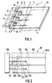
- the flexible electrical connection circuit is, in this example, an electronic card housed in a car.
- the card 1 of the first variant comprises components, not shown, cooled by a radiator 2 fixed on the face of the card 1 opposite to these and which, therefore, stiffens the corresponding part 1A of the card 1.
- Another part 3 of the card 1, comprising an insulating layer, projects beyond the radiator 2 and carries copper tracks on the surface 4 connecting the components above to the pins 5, here aligned, of a connector 6 secured to a housing 7, shown diagrammatically, containing the card 1.
- the pins 5 pass through holes in the center of the welding pads 8 situated on the surface of the flexible part 3 and are welded to these areas 8, themselves connected to the tracks 4 by junction zones 9.
- the flexible part 3 can pivot around an axis 10 tangent to the edges of the pads 8 facing the rigid part 1A of the card 1.
- a bending or twisting of the flexible part 3 can also take place along other axes possibly parallel to axis 10, or else along axes not parallel to axis 10, such as axes 11, 12, tangent to the plane of the flexible part 3 at the level of one either of the two tracks 8 at the end of the row of pins 5.
- the flexible part 3 comprises, at its end opposite to the rigid part 1A of the card 1, a sector 13, substantially limited by the row of pads 8 and the axes 11, 12, not liable to be subjected to stresses originating from the rigidified part of the card 1, since the pins 5, welded to the pads 8, have a mechanical inertia preventing any deformation at their level and on the side opposite to that from which the stresses due to the movement of the rigid part 1A originate.
- the tracks 4 are connected to the pads 8 in the sector 13, by bent portions 14 and folded back on themselves in this example, so that the discontinuity of mechanical inertia to bending, between the tracks 8, with pins 5, and the junction zones 9, has no destructive effect, for lack of bending at this point.
- the second variant embodiment differs from the first variant in that the connector has two parallel rows of pins, here in staggered rows, 105 and 115.
- the elements corresponding to those of FIG. 1 bear the same references as these, preceded by the hundred 1.
- the pins 115 are closest to the rigid part 101A of the card 101, while the pins 105, which are closer to the connector 106, are connected, by pads 108, to rectilinear portions 124 of tracks 104 passing between the pins 115
- the pins 115 are welded into metallized holes 118 in the flexible part 103 isolated from the rest of the card 101 and they prevent the propagation towards the connector 106, in the flexible portion 103, of deformations coming from the rigid part 101A of the card. 101.
- the pins 105, 115 surround a reduced portion 123 of the card 101 which is not liable to be subjected to stresses, whatever direction they come from, and effectively stiffen it.
- the double row of pins 105, 115 provides a bending resistant torque which is increased by increasing the lever arm, i.e. the distance separating them, whereas it was limited to the diameter of the pads 8 in the first variant.
- pins 115 could also, like pins 5, be connected to tracks 104. Likewise, mechanical and electrical connections other than solders could be used to connect tracks 4, 104 to pins 5, 105.
Landscapes
- Engineering & Computer Science (AREA)
- Microelectronics & Electronic Packaging (AREA)
- Coupling Device And Connection With Printed Circuit (AREA)
- Multi-Conductor Connections (AREA)
- Combinations Of Printed Boards (AREA)
Claims (5)
- Flexible Schaltung zum Anschließen einer gedruckten Schaltung, die folgendes aufweist: einen flexiblen Träger (3; 103) mit mindestens einem Verbindungsleiter (4; 104), der mit einem leitenden Endbereich (8; 108) zur Verbindung mit einem Verbindungsstift (5; 105) versehen ist, und Aufnahmeeinrichtungen (8; 108; 118) für Versteifungseinrichtungen (5; 105; 115) eines Bereiches (13; 113) des flexiblen Trägers (3; 103), wobei der an den Endbereich (8; 108) angrenzende Leiterbereich (9) sich auf diesem Bereich (13; 113) des flexiblen Trägers (3; 103) erstreckt,
dadurch gekennzeichnet,
daß die Aufnahmeeinrichtungen (8; 108; 118) dafür ausgelegt sind, einen Versteifungsstift (5; 105; 115) aufzunehmen. - Schaltung nach Anspruch 1,
bei der dann, wenn der Verbindungsstift (5) ein Stift zur Versteifung dieses Bereiches (13) des flexiblen Trägers (3) ist, der Leiter (4) sich über mindestens einen gebogenen Leiterabschnitt (14) bis zu dem Bereich (8) zur Verbindung und zur Aufnahme des Stifts (5) erstreckt. - Schaltung nach einem der Ansprüche 1 und 2,
bei der der an den Verbindungsbereich (8) angrenzende Bereich (14) des Leiters (4) auf sich selbst umgebogen ist. - Schaltung nach Anspruch 1,
bei der ein Versteifungsstift (115) vorgesehen ist, der von einem isolierten Bereich (118) aufgenommen ist. - Schaltung nach einem der Ansprüche 1 und 4,
bei der der an den Verbindungsbereich (108) angrenzende Bereich (124) des Leiters (104) geradlinig ist.
Applications Claiming Priority (2)
| Application Number | Priority Date | Filing Date | Title |
|---|---|---|---|
| FR9309012 | 1993-07-22 | ||
| FR9309012A FR2708172B1 (fr) | 1993-07-22 | 1993-07-22 | Circuit flexible de raccordement d'un circuit imprimé. |
Publications (2)
| Publication Number | Publication Date |
|---|---|
| EP0635995A1 EP0635995A1 (de) | 1995-01-25 |
| EP0635995B1 true EP0635995B1 (de) | 1997-12-29 |
Family
ID=9449499
Family Applications (1)
| Application Number | Title | Priority Date | Filing Date |
|---|---|---|---|
| EP19940401675 Expired - Lifetime EP0635995B1 (de) | 1993-07-22 | 1994-07-21 | Flexible Schaltung zur Verbindung von Leiterplatten |
Country Status (4)
| Country | Link |
|---|---|
| EP (1) | EP0635995B1 (de) |
| DE (1) | DE69407503T2 (de) |
| ES (1) | ES2110712T3 (de) |
| FR (1) | FR2708172B1 (de) |
Families Citing this family (3)
| Publication number | Priority date | Publication date | Assignee | Title |
|---|---|---|---|---|
| DE19653360A1 (de) * | 1996-12-20 | 1998-06-25 | Bosch Gmbh Robert | Leiterfolie zur leitenden Verbindung von elektrischen und/oder elektronischen Baukomponenten |
| DE19653361A1 (de) * | 1996-12-20 | 1998-06-25 | Bosch Gmbh Robert | Leiterfolie |
| US6712234B2 (en) * | 2000-02-14 | 2004-03-30 | Ti Group Automotive Systems Technology Center Gmbh | Fuel tank and method for its production |
Family Cites Families (1)
| Publication number | Priority date | Publication date | Assignee | Title |
|---|---|---|---|---|
| FR2673772B1 (fr) * | 1991-03-04 | 1993-06-25 | Itt Composants Instr | Connecteur electrique pour le raccordement d'un cable electrique se presentant sous la forme d'un circuit souple. |
-
1993
- 1993-07-22 FR FR9309012A patent/FR2708172B1/fr not_active Expired - Fee Related
-
1994
- 1994-07-21 EP EP19940401675 patent/EP0635995B1/de not_active Expired - Lifetime
- 1994-07-21 ES ES94401675T patent/ES2110712T3/es not_active Expired - Lifetime
- 1994-07-21 DE DE1994607503 patent/DE69407503T2/de not_active Expired - Fee Related
Also Published As
| Publication number | Publication date |
|---|---|
| DE69407503T2 (de) | 1998-08-13 |
| EP0635995A1 (de) | 1995-01-25 |
| FR2708172A1 (fr) | 1995-01-27 |
| FR2708172B1 (fr) | 1995-09-08 |
| ES2110712T3 (es) | 1998-02-16 |
| DE69407503D1 (de) | 1998-02-05 |
Similar Documents
| Publication | Publication Date | Title |
|---|---|---|
| EP0547979B1 (de) | Koaxialsteckverbinder zum Verbinden zweier Leiterplatten | |
| EP0766338B1 (de) | Multikontakt für Scheibenantenne | |
| WO1999018541A1 (fr) | Procede de fabrication de cartes a puce aptes a assurer un fonctionnement a contact, et sans contact | |
| EP0756355A1 (de) | Elektrischer Steckverbinder zur Verbindung mit den Kontakten einer integrierten gedruckten Schaltung | |
| CN1249835A (zh) | 印刷电路板模件和包含该模件的印刷电路板 | |
| FR2777732A1 (fr) | Agencement de connexion electrique | |
| EP0635995B1 (de) | Flexible Schaltung zur Verbindung von Leiterplatten | |
| EP0350977B1 (de) | Befestigungseinrichtung eines Metallstücks auf einer Platte | |
| EP0359223A1 (de) | Elektrischer Kontakt für mit oberflächenmontierten Bauelementen ausgestatteten Leiterplatten und Leiterplatte mit wenigstens einem solchen Kontakt | |
| US4967042A (en) | System for enhancing current carrying capacity of printed wiring board | |
| EP3206469A1 (de) | Halterungsvorrichtung für mindestens zwei leiterplatten, entsprechendes elektronisches modul und entsprechendes elektronisches system | |
| EP0450996B1 (de) | Anordnung zum Fixieren eines Koaxialkabels und zum Verbinden mit der Masse einer gedruckten Leiterplatte | |
| EP0263729B1 (de) | Verbindungsvorrichtung für einen statischen Leistungsschalter, der mit biegsamen leitenden Anschlüssen versehen ist | |
| FR2675930A1 (fr) | Carte a circuit integre sans contact. | |
| FR2693339A1 (fr) | Procédé de liaison et de fixation de composants à broches sur un circuit imprimé souple, et circuit ainsi obtenu. | |
| FR3119072A1 (fr) | Calculateur de direction comprenant une carte électronique munie d’une zone fonctionnelle et d’une zone de connectique | |
| EP1672691B1 (de) | Elektrisches Verbindungsstück für integrierten Schaltkreis auf einem Hauptträger | |
| EP0023165A1 (de) | Tragplatte für Leitergitter, insbesondere für integriertes Schaltungsgehäuse, und Gehäuse mit solcher Tragplatte | |
| FR2836773A1 (fr) | Dispositif de connexion d'un conducteur electrique a une carte a circuit imprime | |
| FR2862413A1 (fr) | Capteur de mesure a liaisons conductrices sans raideur et procede de fabrication | |
| FR2784260A1 (fr) | Contacts sans soudure entre des pistes decoupees et un circuit imprime | |
| CH721723A2 (fr) | Dispositif de connexion électrique à pinces | |
| FR3143254A1 (fr) | Ensemble electronique comprenant au moins un ressort lamellaire soude a une premiere plaque metallique par liaison de ruban, et en contact avec une deuxieme plaque metallique, et procede sur la base d’un tel ensemble | |
| FR2771890A1 (fr) | Procede de montage en surface d'un boitier hyperfrequence sur un circuit imprime et boitier et circuit imprime pour la mise en oeuvre du procede | |
| FR2640846A1 (fr) | Dispositif d'encapsulation hermetique pour composants electroniques |
Legal Events
| Date | Code | Title | Description |
|---|---|---|---|
| PUAI | Public reference made under article 153(3) epc to a published international application that has entered the european phase |
Free format text: ORIGINAL CODE: 0009012 |
|
| AK | Designated contracting states |
Kind code of ref document: A1 Designated state(s): DE ES GB IT |
|
| 17P | Request for examination filed |
Effective date: 19950218 |
|
| 17Q | First examination report despatched |
Effective date: 19950927 |
|
| GRAG | Despatch of communication of intention to grant |
Free format text: ORIGINAL CODE: EPIDOS AGRA |
|
| GRAH | Despatch of communication of intention to grant a patent |
Free format text: ORIGINAL CODE: EPIDOS IGRA |
|
| GRAH | Despatch of communication of intention to grant a patent |
Free format text: ORIGINAL CODE: EPIDOS IGRA |
|
| GRAA | (expected) grant |
Free format text: ORIGINAL CODE: 0009210 |
|
| AK | Designated contracting states |
Kind code of ref document: B1 Designated state(s): DE ES GB IT |
|
| REF | Corresponds to: |
Ref document number: 69407503 Country of ref document: DE Date of ref document: 19980205 |
|
| REG | Reference to a national code |
Ref country code: ES Ref legal event code: FG2A Ref document number: 2110712 Country of ref document: ES Kind code of ref document: T3 |
|
| GBT | Gb: translation of ep patent filed (gb section 77(6)(a)/1977) |
Effective date: 19980122 |
|
| ITF | It: translation for a ep patent filed | ||
| PLBE | No opposition filed within time limit |
Free format text: ORIGINAL CODE: 0009261 |
|
| STAA | Information on the status of an ep patent application or granted ep patent |
Free format text: STATUS: NO OPPOSITION FILED WITHIN TIME LIMIT |
|
| 26N | No opposition filed | ||
| PGFP | Annual fee paid to national office [announced via postgrant information from national office to epo] |
Ref country code: ES Payment date: 20010709 Year of fee payment: 8 |
|
| PGFP | Annual fee paid to national office [announced via postgrant information from national office to epo] |
Ref country code: GB Payment date: 20010713 Year of fee payment: 8 |
|
| PGFP | Annual fee paid to national office [announced via postgrant information from national office to epo] |
Ref country code: DE Payment date: 20010717 Year of fee payment: 8 |
|
| REG | Reference to a national code |
Ref country code: GB Ref legal event code: IF02 |
|
| PG25 | Lapsed in a contracting state [announced via postgrant information from national office to epo] |
Ref country code: GB Free format text: LAPSE BECAUSE OF NON-PAYMENT OF DUE FEES Effective date: 20020721 |
|
| PG25 | Lapsed in a contracting state [announced via postgrant information from national office to epo] |
Ref country code: ES Free format text: LAPSE BECAUSE OF NON-PAYMENT OF DUE FEES Effective date: 20020722 |
|
| PG25 | Lapsed in a contracting state [announced via postgrant information from national office to epo] |
Ref country code: DE Free format text: LAPSE BECAUSE OF NON-PAYMENT OF DUE FEES Effective date: 20030201 |
|
| GBPC | Gb: european patent ceased through non-payment of renewal fee |
Effective date: 20020721 |
|
| REG | Reference to a national code |
Ref country code: ES Ref legal event code: FD2A Effective date: 20030811 |
|
| PG25 | Lapsed in a contracting state [announced via postgrant information from national office to epo] |
Ref country code: IT Free format text: LAPSE BECAUSE OF NON-PAYMENT OF DUE FEES;WARNING: LAPSES OF ITALIAN PATENTS WITH EFFECTIVE DATE BEFORE 2007 MAY HAVE OCCURRED AT ANY TIME BEFORE 2007. THE CORRECT EFFECTIVE DATE MAY BE DIFFERENT FROM THE ONE RECORDED. Effective date: 20050721 |