EP0631332A1 - Method of manufacturing Y-Ba-Cu-O superconducting thin film - Google Patents
Method of manufacturing Y-Ba-Cu-O superconducting thin film Download PDFInfo
- Publication number
- EP0631332A1 EP0631332A1 EP94109729A EP94109729A EP0631332A1 EP 0631332 A1 EP0631332 A1 EP 0631332A1 EP 94109729 A EP94109729 A EP 94109729A EP 94109729 A EP94109729 A EP 94109729A EP 0631332 A1 EP0631332 A1 EP 0631332A1
- Authority
- EP
- European Patent Office
- Prior art keywords
- voltage
- target
- substrate
- film formation
- film
- Prior art date
- Legal status (The legal status is an assumption and is not a legal conclusion. Google has not performed a legal analysis and makes no representation as to the accuracy of the status listed.)
- Granted
Links
Images

Classifications
-
- C—CHEMISTRY; METALLURGY
- C23—COATING METALLIC MATERIAL; COATING MATERIAL WITH METALLIC MATERIAL; CHEMICAL SURFACE TREATMENT; DIFFUSION TREATMENT OF METALLIC MATERIAL; COATING BY VACUUM EVAPORATION, BY SPUTTERING, BY ION IMPLANTATION OR BY CHEMICAL VAPOUR DEPOSITION, IN GENERAL; INHIBITING CORROSION OF METALLIC MATERIAL OR INCRUSTATION IN GENERAL
- C23C—COATING METALLIC MATERIAL; COATING MATERIAL WITH METALLIC MATERIAL; SURFACE TREATMENT OF METALLIC MATERIAL BY DIFFUSION INTO THE SURFACE, BY CHEMICAL CONVERSION OR SUBSTITUTION; COATING BY VACUUM EVAPORATION, BY SPUTTERING, BY ION IMPLANTATION OR BY CHEMICAL VAPOUR DEPOSITION, IN GENERAL
- C23C14/00—Coating by vacuum evaporation, by sputtering or by ion implantation of the coating forming material
- C23C14/22—Coating by vacuum evaporation, by sputtering or by ion implantation of the coating forming material characterised by the process of coating
- C23C14/34—Sputtering
- C23C14/3435—Applying energy to the substrate during sputtering
-
- C—CHEMISTRY; METALLURGY
- C23—COATING METALLIC MATERIAL; COATING MATERIAL WITH METALLIC MATERIAL; CHEMICAL SURFACE TREATMENT; DIFFUSION TREATMENT OF METALLIC MATERIAL; COATING BY VACUUM EVAPORATION, BY SPUTTERING, BY ION IMPLANTATION OR BY CHEMICAL VAPOUR DEPOSITION, IN GENERAL; INHIBITING CORROSION OF METALLIC MATERIAL OR INCRUSTATION IN GENERAL
- C23C—COATING METALLIC MATERIAL; COATING MATERIAL WITH METALLIC MATERIAL; SURFACE TREATMENT OF METALLIC MATERIAL BY DIFFUSION INTO THE SURFACE, BY CHEMICAL CONVERSION OR SUBSTITUTION; COATING BY VACUUM EVAPORATION, BY SPUTTERING, BY ION IMPLANTATION OR BY CHEMICAL VAPOUR DEPOSITION, IN GENERAL
- C23C14/00—Coating by vacuum evaporation, by sputtering or by ion implantation of the coating forming material
- C23C14/06—Coating by vacuum evaporation, by sputtering or by ion implantation of the coating forming material characterised by the coating material
- C23C14/08—Oxides
- C23C14/087—Oxides of copper or solid solutions thereof
-
- C—CHEMISTRY; METALLURGY
- C23—COATING METALLIC MATERIAL; COATING MATERIAL WITH METALLIC MATERIAL; CHEMICAL SURFACE TREATMENT; DIFFUSION TREATMENT OF METALLIC MATERIAL; COATING BY VACUUM EVAPORATION, BY SPUTTERING, BY ION IMPLANTATION OR BY CHEMICAL VAPOUR DEPOSITION, IN GENERAL; INHIBITING CORROSION OF METALLIC MATERIAL OR INCRUSTATION IN GENERAL
- C23C—COATING METALLIC MATERIAL; COATING MATERIAL WITH METALLIC MATERIAL; SURFACE TREATMENT OF METALLIC MATERIAL BY DIFFUSION INTO THE SURFACE, BY CHEMICAL CONVERSION OR SUBSTITUTION; COATING BY VACUUM EVAPORATION, BY SPUTTERING, BY ION IMPLANTATION OR BY CHEMICAL VAPOUR DEPOSITION, IN GENERAL
- C23C14/00—Coating by vacuum evaporation, by sputtering or by ion implantation of the coating forming material
- C23C14/22—Coating by vacuum evaporation, by sputtering or by ion implantation of the coating forming material characterised by the process of coating
- C23C14/34—Sputtering
- C23C14/35—Sputtering by application of a magnetic field, e.g. magnetron sputtering
-
- H—ELECTRICITY
- H10—SEMICONDUCTOR DEVICES; ELECTRIC SOLID-STATE DEVICES NOT OTHERWISE PROVIDED FOR
- H10N—ELECTRIC SOLID-STATE DEVICES NOT OTHERWISE PROVIDED FOR
- H10N60/00—Superconducting devices
- H10N60/01—Manufacture or treatment
- H10N60/0268—Manufacture or treatment of devices comprising copper oxide
- H10N60/0296—Processes for depositing or forming superconductor layers
- H10N60/0408—Processes for depositing or forming superconductor layers by sputtering
Abstract
Description
- The present invention relates to a method of manufacturing Y-Ba-Cu-O (hereinafter referred to as YBCO) superconducting thin films having excellent crystallinity using a sputtering phenomenon. More particularly, the present invention relates to a method of optimizing film formation conditions so that the composition ratio of Y:Ba:Cu of a film becomes 1:2:3. The film is suitable for use in the electronics field of sensors, electronic devices or the like using thin films.
- The hybrid plasma sputtering method is available as a parallel plate sputtering method for forming Y-Ba-Cu-O type superconducting thin films on substrates. The characteristic feature of the hybrid plasma sputtering method is that a high-frequency voltage is applied to the cathode electrode being superimposed on a DC voltage supplied through a low-path filter which cuts off the high-frequency voltage, wherein a conductive YBCO target is placed on the cathode and sputtered in a low vacuum. According to this method, YBCO thin films having excellent crystallinity can be obtained (see, for example, W.Ito et al., "Highest Crystallinity of a-axis YBCO films by DC-94.92 MHz Hybrid Plasma Magnetron Sputtering", Physica C 204(1993) pp.295-298).
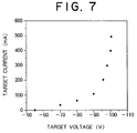
- According to the hybrid plasma sputtering method, when a bias voltage applied from a DC power source is increased at the same time as a high-frequency voltage is applied to the cathode electrode, an electric current increases sharply from a certain voltage, in correspondence with the conductance of a target, and enters into a so-called constant voltage region as shown in Fig. 7. At this time, a DC plasma is superimposed on a high-frequency plasma (hereinafter referred to as a hybrid plasma state). Use of such plasma makes it possible to speed up the film formation while maintaining the advantage of the high-frequency plasma which contributes to crystallinity. Fig. 7 shows the relationship between a bias voltage applied to the cathode and an electric current when a DC voltage and a high-freequency voltage are applied togehter on a YBa₂Cu₃Ox target having a composition ratio of Y:Ba:Cu of 1:2:3. The target voltage is a voltage in which a negative bias voltage generated by a DC power source is superimposed on the self bias on the cathode side generated by the high-frequency plasma which is caused by a high-frequency voltage applied to a YBa₂Cu₃Ox target. The target current is the electric current which flows when the target voltage is applied.
- By optimizing the film formation conditions by using the hybrid plasma sputtering method so that the composition ratio of Y:Ba:Cu of the film becomes 1:2:3, it is possible to manufacture a YBCO thin film whose crystallinity is optimized automatically. An example of the optimized film formation conditions is as follows: the film formation pressure: 475 mTorr, the flow-rate ratio of sputtering gas Ar to reaction gas O2: 2:1, the RF output: 60 W, the cathode voltage: -100 V, and the cathode current: 0.5 A.
- The cathode voltage is the value of the voltage in the constant voltage region of the characteristic shown in Fig. 7. This voltage is dependent on the conductance, or the resistance of the target. Therefore, the value of the cathode voltage in the constant voltage region depends upon the target used. When, for example, a target having a low conductance is used, a voltage drop at the cathode which is necessary for generating a hybrid plasma increases.
- Under the above circumstance, although the optimal film formation conditions for the composition of the film can be obtained, the film has a major problem as to its crystallinity and surface morphology (surface smoothness). The results obtained thus far reveal that, when the cathode voltage in the constant voltage region falls below -100 V by tens of volts, desired crystallinity cannot be obtained even if the composition of the film is optimized by controlling other film formation parameters.
- It can be seen from this that the hybrid plasma sputtering method is a method which is sensitive to, and very restricted with regard to, the conductance of a target used. It seems that the method has a problem as a practical film formation method when the yield of the film with respect to the target is considered.
- The present invention solves the above-described problems of the prior art. It is an object of present invention to provide a method of manufacturing YBCO superconducting thin films capable of manufacturing YBa₂Cu₃Ox superconducting thin films having high crystallinity with a high yield by introducing a new film formation parameter in a hybrid plasma sputtering method.
- According to the present invention, in the above-described hybrid plasma sputtering method, a DC bias (hereinafter referred to as a substrate bias) applied to a substrate holder is introduced as a new film formation parameter, and the film formation conditions are controlled on the basis of a difference between the voltage drops in each ion seath formed on the substrate and directly on the target. As a result, it is possible to provide a YBCO thin film having excellent crystallinity in a high yield with respect to the target.
-
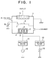
- Fig. 1 is a conceptual view illustrating an example of a film formation apparatus in accordance with an embodiment of the present invention;
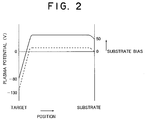
- Fig. 2 shwos the profile of the plasma potential which is developed when a substrate bias of +50 V is applied to a substrate holder of Fig. 1 in accordance with a first embodiment of the present invention;
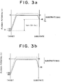
- Figs. 3a and 3b show profiles of the plasma potential which are developed when a negative substrate bias is applied to the substrate holder of Fig. 1 when -40 V and -80 V are applied, respectively, in accordance with the first embodiment of the present invention;
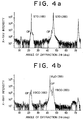
- Figs. 4a and 4b show the X-ray intensity patterns obtained according to an X-ray diffraction method with regard to a YBCO thin film on an SrTiO₃ substrate and an MgO substrate, respectively, which thin film is obtained by using a target #2, in accordance with a second embodiment of the present invention;
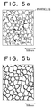
- Figs. 5a and 5b show the surface morphology obtained by observing with a high-resolution scanning electron microscope, illustrating the structure of the film of Fig. 4a and that of Fig. 6a, respectively, in accordance with the second embodiment of the present invention;
- Fig. 6a shows according to an X-ray diffraction method of a YBCO thin film obtained by using a target #2 and applying a substrate bias of -40 V in accordance with the second embodiment of the present invention; and Fig. 6b shows a rocking curve of a peak of a crystal orientation pattern (200) of the film in accordance with the second embodiment of the present invention; and
- Fig. 7 shows the relationship between the bias voltage applied to a cathode and the target current obtained when a DC voltage is applied together with a high-frequency voltage upon a YBa₂Cu₃Ox target.
- Preferred embodiments of the present invention will be described below in detail with reference to the accompanying drawings.
- Fig. 1 is a schematic view illustrating a film formation apparatus according to the present invention. However, the present invention is not limited to this apparatus, and it is possible to modify this apparatus within the scope of the invention.
- In Fig. 1, a mixture gas of argon and oxygen is introduced into a film formation chamber 1 evacuated to the order of 1 x 10⁻⁷ Torr, and a predetermined pressure is formed by controlling the exhaust speed. A
YBCO target 5 having a Y:Ba:Cu composition ratio of 1:2:3 is placed on acathode 4 in which magnets 2 and cooling water passages 3 are provided, and asubstrate 6 is set directly above theYBCO target 5 at a distance of approximately 30 mm there from upon a substrate holder 7. - A
DC power source 8 is connected to the substrate holder 7, and a positive or negative substrate bias can be applied by switching the terminal of thepower source 8. Thesubstrate 6 is heated to a predetermined temperature by aheater 9 on the rear side. A high-frequency (94.92 MHz)power source 10 is connected to thecathode 4 via amatching device 11 so that a high-frequency voltage is applied. At the same time, a negative bias is superimposed on the high-frequency voltage by aDC power source 13 connected via a low-path filter 12. SrTiO₃ and MgO are used for thesubstrate 6. - To use the substrate bias as a parameter for film formation, it is necessary to examine an influence of the polarity of the substrate bias upon the film. The results of the experiment of the substrate bias under the film formation conditions of the total pressure of 475 mTorr, the argon-oxygen ratio of 1:2, the target voltage of -130 V, the target current of 0.5 A, and the substrate temperature of 650C will be explained below.
- When, for example, 50 V is applied to the substrate holder 7 from the
DC power source 8 as a positive substrate bias, it is observed that the electrical potential of theYBCO target 5 side is increased by a magnitude equal to the bias voltage applied to thesubstrate 6 side. The composition and crystallinity of the produced film are the same as those which are formed when no bias is applied. - It is clear from the above that, as shown in Fig. 2, the positive substrate bias translates upwardly the potential profile of a plasma generated between the
substrate 6 and thetarget 5 and does not exert an influence upon plasma particles hitting on thetarget 5 or deposition particles which reach the substrate. Fig. 2 shows the profile characteristic of the plasma potential generated when a substrate bias of +50 V is applied. The characteristic of the plasma potential indicated by the dotted line is the characteristic obtained when theDC power source 8 is set at 0 V and thesubstrate 6 is grounded. The characteristic of the plasma potential indicated by the solid line is the characteristic obtained when a voltage 50 V is applied to the substrate holder 7 by theDC power source 8. - On the other hand, the negative substrate bias showed a substantial effect. Variations in the composition ratio of the film produced when the film formation parameters are fixed and only the negative bias value is varied by the
DC power source 8 are shown in Table 1.Table 1 Bias Voltage (V) Composition Ratio (Y:Ba:Cu) 0 1:1.79:2.23 -40 1:2.26:2.83 -80 1:2.60:4.12 - When an oxide is used as a target in a parallel plate type sputtering, negative ions of oxygen released from the
YBCO target 5 are accelerated by the cathode sheath, causing thesubstrate 6 to be resputtered and the composition of the film to be varied. This effect is well known. Table 1 shows the results obtained when normalization is made using the yttrium (Y) which is least susceptible to resputtering. As the negative bias was increased, an increase of the composition ratio of Cu/Y was most conspicuous. When the fact that Cu is more susceptible to resputtering than Ba or Y is considered, it is clear that the negative substrate bias excludes the negative ions of oxygen and have a tendency to decrease the resputtering effect. - The plasma potential profiles at this time may be presumed to be those of Figs. 3a and 3b on the basis of the observed electrical potentials of the
target 5 and thesubstrate 6. It can be seen that these potential profiles are in agreement with the results of Table 1. In Table 1, when a bias voltage of -40 V was applied as the substrate bias from theDC power source 8, the potential profile shown in Fig. 3a is formed, and when a bias voltage of -80 V is applied, the potential profile shown in Fig. 3b is formed. - In summary, it is clear that the positive substrate bias does not exert an influence upon film formation, whereas the negative substrate bias can be a film formation parameter which decreases the resputtering effect. In the first embodiment, when the negative substrate bias exceeds 150 V, the sputtering of the
substrate 6 by positive ions of argon becomes conspicuous, deteriorating the film. Therefore, the substrate bias is set in a range from 0 to 150 V. If the characteristics of DC plasma are intensified too much in the hybrid plasma sputtering method, it becomes impossible to use the characteristics of the high-frequency plasma. The upper limit of the negative DC voltage applied to thecathode 4 from theDC power source 13 is set at 200 V, and as a result the negative DC current is limited to 1 A or less. - That is, the method has the advantage that an a-axis orientation film having excellent orientation and crystallinity free from a hetero-phase can be obtained without depending upon a target by a method in which a high-frequency voltage and a DC voltage are superimposed on each other and applied to a cathode electrode at the same time, an electroconductive YBCO target is placed on the target, a DC voltage is applied to a substrate holder so that the film formation conditions are controlled on the basis of a difference between voltage drops in each ion sheath formed on the substrate or directly on the target.
- Also, when a film is formed on the basis of a difference between the voltage drops in each ion sheath formed on the substrate or directly on the target, it is possible to always obtain an appropriate voltage drop difference appropriate for the orientation of the film regardless of variations of a voltage drop in the ion sheath formed on the target side by controlling a negative DC voltage applied to the substrate holder in a range from 0 to 150 V. Thus, it is possible to always obtain a YBCO film having stable orientation and crystallinity without being restricted to the target.
- Further, it is possible to use the characteristics of the high-frequency plasma while limiting the intensification of the DC plasma characteristics in the hybrid plasma sputtering method by controlling the negative DC voltage superimposed on a self bias on the cathode side generated by high-frequency plasma resulting from the application of the above high-frequency voltage so that the voltage is in the range from 0 to 200 V, making it possible to obtain desired crystallinity.
- Based on the above-described knowledge, an explanation will be given of the fact that the substrate bias is an effective film formation parameter in the hybrid plasma sputtering method. The details of how problems to be solved are made clean in the hybrid plasma sputtering method will be explained first.
- When the target voltage (the same as the cathode voltage) in a hybrid plasma state is denoted as Vt, this voltage is uniquely determined independently of the other film formation parameters, reflecting the conductance of the
target 5. That is, Vt varies in accordance with the conductance of thetarget 5 placed on thecathode 4. When a target with a low conductance is used, the target voltage Vt increases. - To examine the dependence on the target of the physical properties of the film, a comparative film formation experiment was conducted by using two kinds of targets #1 and #2 having different conductances with a view to manufacturing an a-axis orientation YBa₂Cu₃Ox thin film (the a-axis of the YBa₂Cu₃Ox structure is perpendicular to the substrate)
- When the target #1 was used, the target voltage Vt was -100 V, whereas the voltage was -130 V in the target #2. The film formation conditions under which the composition ratio of the film was optimized with respect to each target are listed in Table 2.
Table 2 Target Film Formation Conditions Crystallinity Target Current and Voltage Total Pressure argon-O₂ Ratio #1 0.5 A -100 V 475 mTorr 1:2 a-axis orientation Δω₂₀₀ < 0.05° #2 0.5 A -130 V 500 mTorr 1:3 a-axis orientation +4Å phase - The reason why the total pressure and the argon-O₂ ratio differ in Table 2 is that the target voltage Vt of each target is reflected. As stated earlier, the hybrid plasma state is achieved when the target voltage enters a constant voltage region. The difference to be noted between the targets #1 and #2 shown in Table 2 is a voltage value at that time. The target voltage of the target #2 entering the constant voltage region is -130 V, which is greater than that in the case of target #1. This is attributable to the fact that the electrical resistance of the target is greater.
- The difference of the film formation conditions for the targets can be explained by the condition of the target voltage. When target #2 having a high target voltage during film formation is used, the acceleration of the negative oxygen ions in the ion sheath formed directly on the
target 5 is promoted. To suppress an increase of the resputtering effect as a result of the above acceleration thereof, the film formation pressure becomes higher than that of target #1. The reason why the electrical resistance of the target is high can be understood when the mixture ratio of argon to oxygen is considered to be attributable to the deficiency of oxygen contained in the target. - The matter to be noted particularly is that the crystallinity or orientation of the film obtained by sputtering two kinds of targets characterized by the above differences of the film formation conditions differs greatly when a target to be sputtered is different in spite of the fact that the composition ratio of Y:Ba:Cu of the film is both 1:2:3.
- A description will now be given of the physical properties of the film obtained from each target.
- When target #1 was used, it was confirmed by an X-ray diffraction method that the crystallinity of the film was optimized automatically by optimizing the composition of the film, and a high-quality a-axis orientation film can be obtained. On the other hand, in the case of target #2, it was confirmed by the same X-ray diffraction method that, as shown in Figs. 4a and 4b, an a-axis orientation (diffraction space or lattice spacing d = 3.90Å) having a diffraction space considerably greater than that of the bulk is exhibited, and a hetero-phase having a diffraction space of 4.090Å appears along a vertical direction.
- Figs. 4a and 4b show the crystal orientation patterns, obtained by an X-ray diffraction method, of a YBCO thin film produced on each of an SrTiO₃ substrate (represented as STO) and an MgO substrate using target #2. Along the horizontal axis is plotted the angle of diffraction, and along the vertical axis is plotted the X-ray intensity. Fig. 4a shows the crystal orientation pattern on the SrTiO₃ substrate, and Fig. 4b shows a crystal orientation pattern on the MgO substrate. Since the peaks of the crystal orientation pattern (n00) of the film on the SrTiO₃ substrate overlap with those of the substrate and hence cannot be confirmed, the results on the MgO substrate are also shown in Fig. 4b in a corresponding manner. The peaks corresponding to the hetero-phase are indicated by OP.
- The method of calculating the a-axis length (the lattice or diffraction space) of YBCO on the MgO substrate will be explained briefly using Fig. 4b as an example. The Bragg's equation is the basic equation of the X-ray diffraction method:

- When the surface morphology was observed with a high-resolution scanning electron microscope, particles which appear to cause the hetero-phase were confirmed (see Fig. 5a). It can be seen that a desired a-axis orientation film cannot be obtained with target #2. Fig. 5a is a schematic view illustrating the structure of the film of Fig. 4a, and Fig. 5b is a schematic view illustrating the structure of the film of Fig. 4b.
- On the basis of the above results, our ideal target is target #1, and target #2 is an inappropriate target. However, it is not possible to always obtain a target such as target #1. Whether the target is appropriate or not can be known when it is disposed in the
cathode 4 and a plasma is generated. Therefore, when a great amount of time required to replace a target and a yield of targets are considered, the hybrid plasma sputtering method has problems as a practical film formation method when applied to manufacturing devices. - According to the second embodiment, however, a new important parameter for film formation was found when a substrate bias experiment was carried out using target #2 in order to solve the above problems.
- The conclusion will be described first. It was found that an a-axis orientation film free from a hetero-phase can be obtained from target #2 in the same manner as when target #1 is used by applying a substrate bias of -40 V from the
DC power source 8. The film formation conditions under the circumstance are: the total pressure of 475 mTorr, the composition ratio of Ar and O₂ gas of 1:3, the target current of 0.5 Å, and the target voltage of -140 V. - The results of the orientation and crystallinity evaluation of the obtained film by an X-ray diffraction method are shown in Figs. 6a and 6b. Fig. 6a shows the X-ray intensity pattern obtained by an X-ray diffraction method with respecy to a YBCO thin film using a target #2 and applying a substrate bias of -40 V, and Fig. 6b shows a rocking curve of the peak of a crystal orientation pattern (200) of the film.
- As can be understood from Fig. 6b, the half-value width of the rocking curve of the peak of the crystal orientation pattern (200) reflecting the crystallinity of the film is recovered to 0.058°, and the surface morphology was improved to one having no particles as can be seen in Fig. 5b.
- The effect of the substrate bias of -40 V will now be discussed, and the gist of the second embodiment is made clear.
- Voltage drops in the ion sheaths formed directly above the cathode 4 (on the
target 5 side) and the anode (on thesubstrate 6 side) are denoted as Vt and Vs, respectively, and the difference between them,


- Not only the negative oxygen ions but also metallic ions, which serve as the deposition seeds, are accelerated in the ion sheaths within which the voltage drop is confined in the plasma. These ions obtain energy necessary for migration on the substrate during this acceleration step, and this energy must be at an appropriate level with respect to the physical properties of the thin film to be manufactured. When this fact and the above-described experimental fact that an a-axis orientation film can be obtained with Vd = 100 V are considered, the condition Vd = 100 V is a necessary condition for obtaining an a-axis orientation film having excellent crystallinity free from a hetero-phase. The condition Vd = 100 V can be achieved by introducing a substrate bias without depending upon the
target 5. - Although the second embodiment describes the a-axis orientation film, this embodiment may be applied to manufacturing a film having other orientations, for example, c-axis orientation films. Since, as described above, the value of Vt varies depending upon the target, it is necessary for the substrate bias applied to obtain Vd appropriate for the orientation of the film to be variable. However, when the negative substrate bias exceeds 150 V, sputtering on the side of the substrate by positive argon ions becomes marked, deteriorating the film. Therefore, the substrate bias should be from 0 to 150 V.
- In the hybrid plasma sputtering method, when the DC plasma characteristics are intensified too much, the characteristics of a high-frequency plasma cannot be utilized. Therefore, the upper limit of a negative DC voltage applied to the
cathode 4 is set at 200 V, and in correspondence with this, the negative DC current is limited to 1 A or less. - When a sputtering pressure is 200 mTorr or less, it is impossible to stop the negative oxygen ions from reaching the substrate even by the substrate bias, causing the film to be resputtered. When the sputtering pressure exceeds 2 Torr, the deposition seed sputtered from the target receives thermal stirring to a greater extent during migration, and it cannot reach the substrate. Therefore, the sputtering pressure should preferably be set at from 200 mTorr to 2 Torr.
- The substrate temperature during film formation is an important film formation parameter for YBCO crystallization in the same manner as in other film formation methods. When the substrate temperature is 600°C or less, the YBCO structure is not formed. When the substrate temperature is 900°C or more, the surface morphology is considerably deteriorated due to redeposition or the like. Therefore, the substrate bias is set at from 600°C to 900°C.
- In the hybrid plasma sputtering method, the intensification of the DC plasma characteristics are limited by limiting a DC current to be superimposed on a self bias on the cathode side, generated by a high-frequency plasma caused by the application of a high-frequency voltage, in the range of more than 0 mA to 1 A or less. Thus, it is possible to use the high-frequency plasma characteristics and obtain desired crystallinity.
- Also, it is possible to prevent the film from being resputtered by blocking the negative oxygen ions from reaching the substrate by forming a film under the condition of the sputtering pressure of 200 mTorr to 2 Torr. Another advantage is that it is possible for the deposition seed to easily reach the substrate sputtered from the target without receiving the thermal stirring during migration.
- Further, YBCO crystallization is made possible while securing a substrate temperature necessary for forming a YBCO structure without deteriorating the surface morphology by forming a film in a temperature range of 600°C to 900°C.
- As described above, it is difficult in the hybrid plasma sputtering method to always manufacture a YBCO thin film having required orientation and crystallinity stably by only controlling film formation parameters as in the past because limitations imposed by the target used are stringent. In other words, the hybrid plasma sputtering method has the problem that the yield of the film with respect to the target is poor. However, according to the above embodiment, the above-described problems are solved by introducing a substrate bias and controlling a new film formation parameter of Vd, which is a difference between the voltage drops in the ion sheaths formed on the substrate and directly on each target. Thus, the method seems to contribute to research into improvements of superconducting characteristics of a thin film and applications thereof into devices in the future.
- A method of manufacturing YBCO superconducting thin films is obtained which is capable of providing superconducting thin films having excellent crystallinity in a high yield by introducing a new film formation parameter in a hybrid plasma sputtering method. When a Y-Ba-Cu-O type superconducting thin film is formed by using a parallel plate sputtering method, a high-frequency voltage generated by a high-frequency power source is superimposed on a DC voltage generated by a DC power source and applied to the cathode electrode at the same time, an electrically conductive YBCO target is placed on the cathode, and the film formation conditions are controlled on the basis of the difference between the voltage drops in each ion sheath formed on the substrate and directly on the target by applying a DC voltage to a substrate holder from the DC power source.
Claims (11)
- A method of manufacturing Y-Ba-Cu-O superconducting thin film on a substrate by using a parallel plate type sputtering method comprising the steps of:
placing an electrically conductive YBCO target on a cathode electrode inside a film formation chamber in a low vacuum and placing said substrate directly above said target via a substrate holder;
superimposing a high-frequency voltage on a negative DC voltage and applying them on said cathode electrode;
applying a negative DC voltage on said substrate holder; and
controlling film formation conditions on the basis of a difference between voltage drop across an ion sheath formed at said substrate and across an ion sheath directly above the YBCO target. - A method according to claim 1 wherein the negative DC voltage which is controlled as one of said film formation conditions and applied to said substrate holder is in a range of from 0 to 150 V.
- A method according to claim 1 wherein said negative DC voltage which is controlled as one of said film formation conditions and superimposed on a self bias of the cathode electrode, generated by a high-frequency plasma caused by said application of said high-frequency voltage, is in a range exceeding 0 and up to 200 V.
- A method according to claim 1 wherein the DC current which is controlled one of as said film formation condition and superimposed a the self bias of said cathode electrode, generated by a high-frequency plasma caused by said application of said high-frequency voltage, is in a range exceeding 0 mA and up to 1 A.
- A method according to claim 1 wherein a sputtering pressure which is controlled as one of said film formation conditions is in a range of from 200 mTorr to 2 Torr.
- A method according to claim 1 wherein the temperature which is controlled as one of said film formation conditions and at which said substrate is heated is in a range of from 600°C to 900°C.
- A method according to claim 1 wherein a hybrid plasma obtained by superimposing a DC plasma generated by applying a negative DC voltage on a high-frequency plasma generated by applying said high-frequency voltage is used to form a film.
- A method according to claim 1 wherein said YBCO target is a YBa₂Cu₃Ox target in which a composition ratio of Y:Ba:Cu is adjusted to 1:2:3.
- A method according to claim 1 wherein said substrate is made of one selecy from the group consisting of SrTiO₃ and MgO.
- A method according to claim 1 wherein a mixture gas of argon and oxygen is introduced into said film formation chamber.
- A method according to claim 1 wherein said difference between said voltage drops across said ion sheath formed at said substrate and across said ion sheath directly above said YBCO target is controlled to 100 V, thereby obtaining an a-axis orientation film.
Applications Claiming Priority (2)
| Application Number | Priority Date | Filing Date | Title |
|---|---|---|---|
| JP5153824A JPH0715051A (en) | 1993-06-24 | 1993-06-24 | Manufacture of ybco superconducting thin film |
| JP153824/93 | 1993-06-24 |
Publications (2)
| Publication Number | Publication Date |
|---|---|
| EP0631332A1 true EP0631332A1 (en) | 1994-12-28 |
| EP0631332B1 EP0631332B1 (en) | 1997-04-16 |
Family
ID=15570898
Family Applications (1)
| Application Number | Title | Priority Date | Filing Date |
|---|---|---|---|
| EP94109729A Expired - Lifetime EP0631332B1 (en) | 1993-06-24 | 1994-06-23 | Method of manufacturing Y-Ba-Cu-O superconducting thin film |
Country Status (4)
| Country | Link |
|---|---|
| US (1) | US5466665A (en) |
| EP (1) | EP0631332B1 (en) |
| JP (1) | JPH0715051A (en) |
| DE (1) | DE69402619T2 (en) |
Cited By (1)
| Publication number | Priority date | Publication date | Assignee | Title |
|---|---|---|---|---|
| EP1905867A1 (en) * | 2006-09-28 | 2008-04-02 | Fujifilm Corporation | Process for forming a film, piezoelectric film, and piezoelectric device |
Families Citing this family (5)
| Publication number | Priority date | Publication date | Assignee | Title |
|---|---|---|---|---|
| US20030094239A1 (en) * | 2000-06-02 | 2003-05-22 | Quon Bill H. | Apparatus and method for improving electron ecceleration |
| US6413380B1 (en) * | 2000-08-14 | 2002-07-02 | International Business Machines Corporation | Method and apparatus for providing deposited layer structures and articles so produced |
| WO2009014394A2 (en) * | 2007-07-25 | 2009-01-29 | Nuricell, Inc. | Method for depositing ceramic thin film by sputtering using non-conductive target |
| US8540851B2 (en) * | 2009-02-19 | 2013-09-24 | Fujifilm Corporation | Physical vapor deposition with impedance matching network |
| CN112962076B (en) * | 2021-02-04 | 2022-04-05 | 西南交通大学 | Preparation method of metal precursor film of second-generation high-temperature superconducting tape |
Citations (3)
| Publication number | Priority date | Publication date | Assignee | Title |
|---|---|---|---|---|
| EP0347567A2 (en) * | 1988-06-23 | 1989-12-27 | Leybold Aktiengesellschaft | Device for coating a substrate with a dielectric |
| EP0462906A2 (en) * | 1990-06-21 | 1991-12-27 | Sumitomo Electric Industries, Ltd. | Process and apparatus for preparing superconducting thin films |
| EP0587095A2 (en) * | 1992-09-07 | 1994-03-16 | Nippon Steel Corporation | Method of making an oxide superconducting thin film |
Family Cites Families (7)
| Publication number | Priority date | Publication date | Assignee | Title |
|---|---|---|---|---|
| US3461054A (en) * | 1966-03-24 | 1969-08-12 | Bell Telephone Labor Inc | Cathodic sputtering from a cathodically biased target electrode having an rf potential superimposed on the cathodic bias |
| KR0132061B1 (en) * | 1987-03-14 | 1998-04-24 | 나까하라 쯔네오 | Process for depositing a superconducting thin film |
| US5236894A (en) * | 1987-12-26 | 1993-08-17 | Sumitomo Electric Industries, Ltd. | Process for producing a superconducting thin film at relatively low temperature |
| US5361720A (en) * | 1988-04-22 | 1994-11-08 | British Technology Group Ltd. | Epitaxial deposition |
| JP2936276B2 (en) * | 1990-02-27 | 1999-08-23 | 日本真空技術株式会社 | Method and apparatus for manufacturing transparent conductive film |
| JPH04219301A (en) * | 1990-07-25 | 1992-08-10 | Semiconductor Energy Lab Co Ltd | Production of oxide superconductor thin film |
| ATE144004T1 (en) * | 1991-04-12 | 1996-10-15 | Balzers Hochvakuum | METHOD AND SYSTEM FOR COATING AT LEAST ONE OBJECT |
-
1993
- 1993-06-24 JP JP5153824A patent/JPH0715051A/en active Pending
-
1994
- 1994-06-16 US US08/263,957 patent/US5466665A/en not_active Expired - Fee Related
- 1994-06-23 EP EP94109729A patent/EP0631332B1/en not_active Expired - Lifetime
- 1994-06-23 DE DE69402619T patent/DE69402619T2/en not_active Expired - Fee Related
Patent Citations (3)
| Publication number | Priority date | Publication date | Assignee | Title |
|---|---|---|---|---|
| EP0347567A2 (en) * | 1988-06-23 | 1989-12-27 | Leybold Aktiengesellschaft | Device for coating a substrate with a dielectric |
| EP0462906A2 (en) * | 1990-06-21 | 1991-12-27 | Sumitomo Electric Industries, Ltd. | Process and apparatus for preparing superconducting thin films |
| EP0587095A2 (en) * | 1992-09-07 | 1994-03-16 | Nippon Steel Corporation | Method of making an oxide superconducting thin film |
Non-Patent Citations (2)
| Title |
|---|
| ITO W ET AL: "Effects of substrate ion sheath during sputtering on the superconductivity of a-axis YBCO films", PHYSICA C, 1 MAY 1994, NETHERLANDS, VOL. 224, NR. 3-4, PAGE(S) 384 - 390, ISSN 0921-4534 * |
| NAKAGAWA A ET AL: "Substrate bias and pressure effect on formation of YBaCuO thin films in RF magnetron sputtering system", JAPANESE JOURNAL OF APPLIED PHYSICS, PART 2 (LETTERS), 1 JUNE 1991, JAPAN, VOL. 30, NR. 6A, PAGE(S) L993 - L996, ISSN 0021-4922 * |
Cited By (1)
| Publication number | Priority date | Publication date | Assignee | Title |
|---|---|---|---|---|
| EP1905867A1 (en) * | 2006-09-28 | 2008-04-02 | Fujifilm Corporation | Process for forming a film, piezoelectric film, and piezoelectric device |
Also Published As
| Publication number | Publication date |
|---|---|
| DE69402619T2 (en) | 1997-09-18 |
| US5466665A (en) | 1995-11-14 |
| JPH0715051A (en) | 1995-01-17 |
| EP0631332B1 (en) | 1997-04-16 |
| DE69402619D1 (en) | 1997-05-22 |
Similar Documents
| Publication | Publication Date | Title |
|---|---|---|
| US5977582A (en) | Capacitor comprising improved TaOx -based dielectric | |
| EP0905723B1 (en) | Amorphous dielectric materials and capacitors employing the same | |
| EP0441408B1 (en) | Process for producing a ferroelectric film | |
| EP0631332A1 (en) | Method of manufacturing Y-Ba-Cu-O superconducting thin film | |
| JPH09176850A (en) | Sputtering device and production of dielectric film | |
| JPH05147933A (en) | Amorphous ferroelectric oxide material and its production | |
| JP3831433B2 (en) | Transparent conductive film and method for producing the same | |
| JPH05147936A (en) | Amorphous ferroelectric oxide material and its production | |
| JPH05139730A (en) | Amorphous ferroelectric oxide material and production thereof | |
| JPH05147940A (en) | Amorphous ferroelectric oxide material and its production | |
| Grigorov et al. | Layered structures HTSC/ferroelectric, prepared by sputtering | |
| EP0321071A1 (en) | Method of producing superconducting thin films | |
| JPH05147927A (en) | Amorphous ferroelectric oxide material and its production | |
| JPH05151823A (en) | Amorphous ferroelectric oxide material and manufacture thereof | |
| JPH05105431A (en) | Amorphous ferroelectric oxide material and its manufacture | |
| JPH05147935A (en) | Amorphous ferroelectric oxide material and its production | |
| JPH0517127A (en) | Amorphous ferroelectric oxide material and its production | |
| JPH05109315A (en) | Amorphous ferroelectric oxide material and its manufacture | |
| JPH05105440A (en) | Amorphous ferroelectric oxide material and its manufacture | |
| JPH05132313A (en) | Amorphous ferroelectric oxide material and its production | |
| JPH05105438A (en) | Amorphous ferroelectric oxide material and its manufacture | |
| JPH05132316A (en) | Amorphous ferroelectric oxide material and its production | |
| JPH05147939A (en) | Amorphous ferroelectric oxide material and its production | |
| JPH05105422A (en) | Amorphous ferroelectric oxide material and its manufacture | |
| JPH05105437A (en) | Amorphous ferroelectric oxide material and its manufacture |
Legal Events
| Date | Code | Title | Description |
|---|---|---|---|
| PUAI | Public reference made under article 153(3) epc to a published international application that has entered the european phase |
Free format text: ORIGINAL CODE: 0009012 |
|
| AK | Designated contracting states |
Kind code of ref document: A1 Designated state(s): DE FR GB |
|
| 17P | Request for examination filed |
Effective date: 19950427 |
|
| 17Q | First examination report despatched |
Effective date: 19951121 |
|
| GRAG | Despatch of communication of intention to grant |
Free format text: ORIGINAL CODE: EPIDOS AGRA |
|
| GRAH | Despatch of communication of intention to grant a patent |
Free format text: ORIGINAL CODE: EPIDOS IGRA |
|
| GRAH | Despatch of communication of intention to grant a patent |
Free format text: ORIGINAL CODE: EPIDOS IGRA |
|
| GRAA | (expected) grant |
Free format text: ORIGINAL CODE: 0009210 |
|
| AK | Designated contracting states |
Kind code of ref document: B1 Designated state(s): DE FR GB |
|
| REF | Corresponds to: |
Ref document number: 69402619 Country of ref document: DE Date of ref document: 19970522 |
|
| ET | Fr: translation filed | ||
| PLBE | No opposition filed within time limit |
Free format text: ORIGINAL CODE: 0009261 |
|
| STAA | Information on the status of an ep patent application or granted ep patent |
Free format text: STATUS: NO OPPOSITION FILED WITHIN TIME LIMIT |
|
| 26N | No opposition filed | ||
| REG | Reference to a national code |
Ref country code: GB Ref legal event code: IF02 |
|
| REG | Reference to a national code |
Ref country code: GB Ref legal event code: 732E |
|
| REG | Reference to a national code |
Ref country code: GB Ref legal event code: 732E |
|
| PGFP | Annual fee paid to national office [announced via postgrant information from national office to epo] |
Ref country code: FR Payment date: 20060608 Year of fee payment: 13 |
|
| PGFP | Annual fee paid to national office [announced via postgrant information from national office to epo] |
Ref country code: DE Payment date: 20060615 Year of fee payment: 13 |
|
| PGFP | Annual fee paid to national office [announced via postgrant information from national office to epo] |
Ref country code: GB Payment date: 20060621 Year of fee payment: 13 |
|
| REG | Reference to a national code |
Ref country code: FR Ref legal event code: TQ |
|
| GBPC | Gb: european patent ceased through non-payment of renewal fee |
Effective date: 20070623 |
|
| REG | Reference to a national code |
Ref country code: FR Ref legal event code: ST Effective date: 20080229 |
|
| PG25 | Lapsed in a contracting state [announced via postgrant information from national office to epo] |
Ref country code: DE Free format text: LAPSE BECAUSE OF NON-PAYMENT OF DUE FEES Effective date: 20080101 |
|
| PG25 | Lapsed in a contracting state [announced via postgrant information from national office to epo] |
Ref country code: GB Free format text: LAPSE BECAUSE OF NON-PAYMENT OF DUE FEES Effective date: 20070623 |
|
| PG25 | Lapsed in a contracting state [announced via postgrant information from national office to epo] |
Ref country code: FR Free format text: LAPSE BECAUSE OF NON-PAYMENT OF DUE FEES Effective date: 20070702 |