EP0630044B1 - Forming a prescribed pattern on a semiconducor device layer - Google Patents
Forming a prescribed pattern on a semiconducor device layer Download PDFInfo
- Publication number
- EP0630044B1 EP0630044B1 EP94114930A EP94114930A EP0630044B1 EP 0630044 B1 EP0630044 B1 EP 0630044B1 EP 94114930 A EP94114930 A EP 94114930A EP 94114930 A EP94114930 A EP 94114930A EP 0630044 B1 EP0630044 B1 EP 0630044B1
- Authority
- EP
- European Patent Office
- Prior art keywords
- layer
- forming
- glass
- pattern
- photoresist
- Prior art date
- Legal status (The legal status is an assumption and is not a legal conclusion. Google has not performed a legal analysis and makes no representation as to the accuracy of the status listed.)
- Expired - Lifetime
Links
Images

Classifications
-
- H—ELECTRICITY
- H10—SEMICONDUCTOR DEVICES; ELECTRIC SOLID-STATE DEVICES NOT OTHERWISE PROVIDED FOR
- H10P—GENERIC PROCESSES OR APPARATUS FOR THE MANUFACTURE OR TREATMENT OF DEVICES COVERED BY CLASS H10
- H10P14/00—Formation of materials, e.g. in the shape of layers or pillars
- H10P14/60—Formation of materials, e.g. in the shape of layers or pillars of insulating materials
- H10P14/63—Formation of materials, e.g. in the shape of layers or pillars of insulating materials characterised by the formation processes
- H10P14/6326—Deposition processes
- H10P14/6342—Liquid deposition, e.g. spin-coating, sol-gel techniques or spray coating
-
- H—ELECTRICITY
- H10—SEMICONDUCTOR DEVICES; ELECTRIC SOLID-STATE DEVICES NOT OTHERWISE PROVIDED FOR
- H10P—GENERIC PROCESSES OR APPARATUS FOR THE MANUFACTURE OR TREATMENT OF DEVICES COVERED BY CLASS H10
- H10P14/00—Formation of materials, e.g. in the shape of layers or pillars
- H10P14/60—Formation of materials, e.g. in the shape of layers or pillars of insulating materials
- H10P14/61—Formation of materials, e.g. in the shape of layers or pillars of insulating materials using masks
-
- H—ELECTRICITY
- H10—SEMICONDUCTOR DEVICES; ELECTRIC SOLID-STATE DEVICES NOT OTHERWISE PROVIDED FOR
- H10P—GENERIC PROCESSES OR APPARATUS FOR THE MANUFACTURE OR TREATMENT OF DEVICES COVERED BY CLASS H10
- H10P14/00—Formation of materials, e.g. in the shape of layers or pillars
- H10P14/60—Formation of materials, e.g. in the shape of layers or pillars of insulating materials
- H10P14/69—Inorganic materials
- H10P14/692—Inorganic materials composed of oxides, glassy oxides or oxide-based glasses
- H10P14/6921—Inorganic materials composed of oxides, glassy oxides or oxide-based glasses containing silicon
- H10P14/69215—Inorganic materials composed of oxides, glassy oxides or oxide-based glasses containing silicon the material being a silicon oxide, e.g. SiO2
-
- H—ELECTRICITY
- H10—SEMICONDUCTOR DEVICES; ELECTRIC SOLID-STATE DEVICES NOT OTHERWISE PROVIDED FOR
- H10P—GENERIC PROCESSES OR APPARATUS FOR THE MANUFACTURE OR TREATMENT OF DEVICES COVERED BY CLASS H10
- H10P50/00—Etching of wafers, substrates or parts of devices
- H10P50/71—Etching of wafers, substrates or parts of devices using masks for conductive or resistive materials
-
- H—ELECTRICITY
- H10—SEMICONDUCTOR DEVICES; ELECTRIC SOLID-STATE DEVICES NOT OTHERWISE PROVIDED FOR
- H10P—GENERIC PROCESSES OR APPARATUS FOR THE MANUFACTURE OR TREATMENT OF DEVICES COVERED BY CLASS H10
- H10P50/00—Etching of wafers, substrates or parts of devices
- H10P50/73—Etching of wafers, substrates or parts of devices using masks for insulating materials
-
- H—ELECTRICITY
- H10—SEMICONDUCTOR DEVICES; ELECTRIC SOLID-STATE DEVICES NOT OTHERWISE PROVIDED FOR
- H10P—GENERIC PROCESSES OR APPARATUS FOR THE MANUFACTURE OR TREATMENT OF DEVICES COVERED BY CLASS H10
- H10P76/00—Manufacture or treatment of masks on semiconductor bodies, e.g. by lithography or photolithography
- H10P76/40—Manufacture or treatment of masks on semiconductor bodies, e.g. by lithography or photolithography of masks comprising inorganic materials
- H10P76/405—Manufacture or treatment of masks on semiconductor bodies, e.g. by lithography or photolithography of masks comprising inorganic materials characterised by their composition, e.g. multilayer masks
-
- H—ELECTRICITY
- H10—SEMICONDUCTOR DEVICES; ELECTRIC SOLID-STATE DEVICES NOT OTHERWISE PROVIDED FOR
- H10P—GENERIC PROCESSES OR APPARATUS FOR THE MANUFACTURE OR TREATMENT OF DEVICES COVERED BY CLASS H10
- H10P76/00—Manufacture or treatment of masks on semiconductor bodies, e.g. by lithography or photolithography
- H10P76/40—Manufacture or treatment of masks on semiconductor bodies, e.g. by lithography or photolithography of masks comprising inorganic materials
- H10P76/408—Manufacture or treatment of masks on semiconductor bodies, e.g. by lithography or photolithography of masks comprising inorganic materials characterised by their sizes, orientations, dispositions, behaviours or shapes
- H10P76/4085—Manufacture or treatment of masks on semiconductor bodies, e.g. by lithography or photolithography of masks comprising inorganic materials characterised by their sizes, orientations, dispositions, behaviours or shapes characterised by the processes involved to create the masks
-
- H—ELECTRICITY
- H10—SEMICONDUCTOR DEVICES; ELECTRIC SOLID-STATE DEVICES NOT OTHERWISE PROVIDED FOR
- H10W—GENERIC PACKAGES, INTERCONNECTIONS, CONNECTORS OR OTHER CONSTRUCTIONAL DETAILS OF DEVICES COVERED BY CLASS H10
- H10W20/00—Interconnections in chips, wafers or substrates
- H10W20/01—Manufacture or treatment
- H10W20/031—Manufacture or treatment of conductive parts of the interconnections
-
- H—ELECTRICITY
- H10—SEMICONDUCTOR DEVICES; ELECTRIC SOLID-STATE DEVICES NOT OTHERWISE PROVIDED FOR
- H10W—GENERIC PACKAGES, INTERCONNECTIONS, CONNECTORS OR OTHER CONSTRUCTIONAL DETAILS OF DEVICES COVERED BY CLASS H10
- H10W20/00—Interconnections in chips, wafers or substrates
- H10W20/01—Manufacture or treatment
- H10W20/071—Manufacture or treatment of dielectric parts thereof
- H10W20/081—Manufacture or treatment of dielectric parts thereof by forming openings in the dielectric parts
Definitions
- This invention concerns a method for forming a prescribed pattern of, e.g., a wiring layer by etching, on a semiconductor device.
- RIE Reactive Ion Etching
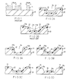
- FIG.1 is a diagram for explaining a problem which is present in a conventional process for forming a pattern of submicron dimensions using a conventional exposure and development technique.
- the width between the adjacent pattern is relatively wide, e.g. 1.0 ⁇ m
- a desired pattern may be obtained by the conventional technique.
- the width is 0.8 ⁇ m (e.g., between the photoresist pattern 12 and 13 )
- some undeveloped photoresist remains on the substrate 10 , since the bottom portion of the photoresist is not sufficiently exposed even if the upper portion is clearly patterned.
- FIGS.2A and 2B are diagrams for explaining a problem in a conventional process for forming a prescribed pattern of a high reflective metal layer 21 in a recessed portion 24 of a semiconductor substrate 20 .
- a material of high reflectivity such as a tungsten silicide 21
- a photoresist layer 23 is then formed thereon (Fig. 2A).
- an exposure and a development are carried out to form a photoresist pattern 23a and 23b.
- a desired pattern 23a and 23b of photoresist may be formed on a flat surface of the substrate 20.
- the reflected light from the angled surface 22 of the metal layer 21 exposes the photoresist 23 in the recess.
- the desired pattern illustrated by the dotted line 23c cannot be obtained, and a photoresist pattern 23d may result instead. Therefore, it is also difficult to use the pattern 23d as a mask to etch the metal layer 21 accurately.
- U.S. Patent No. 4599137 It is known from U.S. Patent No. 4599137 to provide a method, as defined in the pre-characterizing portion of Claim 1, of forming a resist micropattern in a semiconductor device manufacturing process. Further, U.S. Patent No. 4624 749 discloses the use of a metal (gold) as an interconnect layer, formed by gold-electroplating selectively over a photoresist pattern which is complementary to the desired gold interconnect pattern.
- An object of the present invention is to provide an improved method which results in a desired accurate photoresist pattern, even if the width between the adjacent portions of the pattern is of the submicron order.
- this invention provides a method as defined in Claim 1 for forming a prescribed pattern on a layer of a semiconductor device.
- FIG. 1 is a cross sectional view for explaining a problem in a conventional process.
- FIGS. 2A and 2B are drawings for explaining another conventional process and the problem inherent therein.
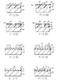
- FIGS. 4A to 4D and FIGS. 5A to 5E are cross sectional views for explaining embodiments of the present invention.
- FIGS. 3A to 3D, FIGS. 6A to 6D and FIGS 7A to 7D are cross sectional views of structures made using a method outside the scope of the present invention.
- FIGS. 3A to 3D are cross sectional views for explaining an embodiment of the invention of our parent application EP-A-358350, which is outside the scope of the present application, but is included as background. It allows formation of a wiring pattern at a recessed portion of a semiconductor substrate.
- a semiconductor substrate 30 having a recessed portion or a dent 34 is prepared. Then, a tungsten silicide layer 31 to be patterned is formed on the substrate 30 . Next, a positive photoresist layer, e.g., an OFPR (manufactured by Tokyo Oka Co.), is formed over the entire surface, and a photoresist pattern 33a and 33b covering a wall 32 at the dent 34 is formed using a conventional exposure and development technique. (FIG.3A)
- OFPR manufactured by Tokyo Oka Co.
- the substrate 30 is immersed into a silicofluoride aqueous solution.
- a silicon oxide (SiO2) layer 35 of about 1000 A is selectively formed at the area where the tungsten silicide (WSi) layer 31 is exposed, since the H2SiF6 and H20 react to precipitate SiO2.
- the surface of the photoresist layer 33a and 33b are subjected to, e.g., an oxygen plasma, to change the surface thereof from a hydrophilic condition (having, e.g., -OH radical as an end radical) to a hydrophobic condition (having, e.g., -O radical as an end radical), preferably, ( FIG.3B )
- a hydrophilic condition having, e.g., -OH radical as an end radical
- a hydrophobic condition having, e.g., -O radical as an end radical
- the photoresist pattern 33a and 33b are removed by, e.g., an ashing ( FIG.3C )
- an anisotropic etching such as a RIE
- RIE etching for removing the SiO2 layer 35 follows thereafter (not shown)
- the wall 32 at the dent 34 is not exposed.
- the problem due to the light reflection from the surface 32 can be prevented.
- the etching selectively between the WSi and the SiO2 is relatively high. Therefore, it is possible to obtain a desired pattern of WSi wiring 31a on the substrate 30, even if the substrate 30 includes a recessed portion, since the SiO2 layer 35 having a relatively low etching rate is used as a mask to etch the WSi layer 31.
- FIGS. 4A to 4D are cross sectional views.
- a thermal oxide layer 41 is formed on a semiconductor substrate 40.
- an aluminium layer (A1) 42 of about 8000 ⁇ to be etched is formed by, e.g., sputtering.
- a patterned photoresist pattern 43 of about 12,000 ⁇ is formed on the A1 layer 42 using a conventional exposure and development technique.
- a glass layer 44 is formed by a Spin on Glass (SOG) method following a baking treatment. (FIG.
- a conventional etching process is carried out to remove the relatively thin glass layer formed on the photoresist 43, and to leave a portion of the relatively thick glass layer 44 formed where the photoresist layer 43 is not formed.
- a hydrophobic treatment is carried out.
- the photoresist pattern 43 is removed by, e. g., a wet etching. (FIG. 4C)
- an anisotropic etching e.g., a RIE
- a RIE anisotropic etching
- an etching for removing the SiO2 layer 45 and the glass layer 44 is carried out (not shown).
- the etching selectivity between the A1 layer and the SiO2 layer is about 10, and is relatively large compared with that of between the A1 layer and the photoresist layer, namely about 2.
- the selectivity of the etching can be improved.
- the remaining A1 pattern 42a and 42b is determined by the SiO2 layer 45 .
- the area where the SiO2 layer is formed is determined by the remaining photoresist layer 43.
- the glass layer 44 serves to protect the A1 layer 42 from etching during the immersion of the substrate into the solution for precipitating the SiO2 layer 45 .
- FIGS.5A to 5E are drawings of a further example.
- a thermal oxide layer 51 is formed on the oxide layer 51 .
- a aluminium layer (A1) 52 of about 8,000 ⁇ to be etched is formed by, e.g., a sputtering.
- a glass layer 53 is formed by a Spin on Glass method following a baking treatment.
- a patterned photoresist layer 54a, 54b and 54c is formed using a conventional exposure and development technique.
- the substrate After a hydrophobic treatment of the photoresist pattern 54, the substrate is immersed into a silicofluoride aqueous solution to form a SiO2 layer 55. ( FIG.5B )
- an etching e.g., a wet etching, is carried out to etch the glass layer 53 using the SiO2 layer 55 as a mask.
- etching e.g., a wet etching
- an anisotropic etching e.g., a RIE etching
- a desired Al wiring layer 52a and 52b using the SiO2 layer 55 as a mask.
- FIG.5E the glass layer 53 and the SiO2 layer 55 are removed (not shown).
- a desired wiring pattern can be achieved, as in the example illustrated in FIGS.4A to 4D .
- FIGS.6A to 6D are drawings for explaining a further example, outside the scope of the present invention, of forming a contact hole in a semiconductor device.
- an insulating layer 61 is formed on a semiconductor substrate 60 .
- a polysilicon layer 62 of about 300 ⁇ is formed on the insulating layer by, e.g., a low pressure CVD method.
- a patterned photoresist layer 63 is formed on the polysilicon layer 62 using a conventional exposure and development technique. ( FIG.6A )
- a hydrophobic treatment of the photoresist layer 63 is carried out.
- the substrate is immersed into a solution of palladium chloride (PbCl2) to form a palladium layer 64 of less than 100 ⁇ using a non-electric plating method.
- the substrate is immersed into a mixed solution of nickel sulfate (NiSO4) and hypophosphite to form a nickel layer 65 of about 1000 ⁇ .
- NiSO4 nickel sulfate
- the photoresist layer is removed by, e.g., an ashing treatment using an oxygen plasma.
- FIG.6C shows an ashing treatment using an oxygen plasma.
- an anisotropic etching e.g., a RIE, is carried out to form a contact hole 66 using the nickel layer 65 as a mask.
- a RIE anisotropic etching
- the nickel layer 65 and the palladium layer 64 are removed by a wet etching using a mixed etchant of a hydrochloric acid, a nitric acid and an acetic acid.
- the polysilicon layer 62 may either be removed by a wet etching using an organic alkali solution, e.g., a choline or a dry etching using a fluorine as an active radical, or it may be oxidized and left as it is.
- the size of the contact hole 66 is determined by the remaining photoresist pattern 63 .
- the size of the photoresist layer 63 is determined by the remaining photoresist pattern 63 .
- the etching rate of the nickel layer 65 is extremely smaller than that of the insulating layer 61 .
- the palladium layer 64 provides a good adhesion between the polysilicon layer 62 and the nickel layer 65.
- FIGS.7A to 7D are drawings for explaining a further example, outside the scope of the present invention, of oxidizing a semiconductor substrate 70 .
- a thermal insulating layer 71 is formed on a semiconductor substrate 70 .
- a silicon nitride layer 72 is formed on the insulating layer 71.
- a patterned photoresist layer 73 is formed on the silicon nitride layer 72 .
- the substrate After a hydrophobic treatment of the photoresist layer 73 , the substrate is immersed into the same solution, in the same way, as the embodiment of FIGS.3A to 3D, to form a SiO2 layer 74.
- the photoresist layer 73 is removed by, e.g., ashing using an oxygen plasma. ( FIG.7C )
- the silicon nitride layer 72 is selectively etched by using the SiO2 layer 74 as a mask.
- An oxidizing treatment is then carried out to oxidize the substrate 70 to form a device separating oxide layer 75 , using the silicon nitride layer 72 selectively remaining under the SiO2 layer 74 as a mask layer.
- an etching treatment e.g., a Chemical Dry Etching (CDE) is carried out to remove the SiO2 layer 74 and the silicon nitride layer 72 .
- CDE Chemical Dry Etching
- a SiO2 layer formed by a precipitation is used as a mask layer.
Landscapes
- Internal Circuitry In Semiconductor Integrated Circuit Devices (AREA)
- Drying Of Semiconductors (AREA)
- Liquid Deposition Of Substances Of Which Semiconductor Devices Are Composed (AREA)
- Weting (AREA)
Description
Namely, in the case where the width between the adjacent pattern is relatively wide, e.g. 1.0 µm, a desired pattern may be obtained by the conventional technique. However, in the case where the width is 0.8 µm (e.g., between the
Claims (6)
- A method of forming a prescribed pattern on a layer of a semiconductor device, comprising the steps of:characterised in that the first layer (41) is an insulating layer, the second layer (42) is a metal layer, third layer (43) is a photoresist layer, and the fourth layer is a SiO2 layer, whereby the remainder of the second layer (42) constitutes a metal interconnect layer for the semiconductor device.preparing a substrate (40) having a first main surface;forming a first layer (41) on the first main surface;forming a second layer (42) on the first layer;forming a third layer (43) on the second layer;selectively removing the third layer to form a first patterned layer;immersing the substrate having the first patterned layer into a predetermined solution to form a fourth layer (45) selectively over the portions of the second layer not covered by the first patterned layer;removing the first patterned layer; andetching the second layer using the fourth layer (45) as a mask,
- A method according to Claim 1, further comprising the step of forming a glass layer (44) on the second layer (42) before the formation of the fourth layer (45).
- A method according to Claim 2, wherein the glass layer (44) is formed by a Spin on Glass method.
- A method according to Claim 2 or 3, comprising the step of etching away the portions of the glass layer (44) overlying the third layer (43), before the step of immersing the substrate.
- A method according to Claim 4, comprising hydrophobic treatment of the third layer (43) immediately following the said step of etching away of portions of the glass layer (44).
- A method according to any preceding claim, further comprising the step of forming the glass layer (53) as the upper layer of the second layer (52) before the formation of the third layer (54), so that the glass layer is etched using the fourth layer (55) as a mask.
Applications Claiming Priority (3)
| Application Number | Priority Date | Filing Date | Title |
|---|---|---|---|
| JP63223503A JP2606900B2 (en) | 1988-09-08 | 1988-09-08 | Pattern formation method |
| JP223503/88 | 1988-09-08 | ||
| EP89308284A EP0358350B1 (en) | 1988-09-08 | 1989-08-15 | Forming a Prescribed Pattern on a Semiconductor Device Layer |
Related Parent Applications (1)
| Application Number | Title | Priority Date | Filing Date |
|---|---|---|---|
| EP89308284A Division EP0358350B1 (en) | 1988-09-08 | 1989-08-15 | Forming a Prescribed Pattern on a Semiconductor Device Layer |
Publications (3)
| Publication Number | Publication Date |
|---|---|
| EP0630044A2 EP0630044A2 (en) | 1994-12-21 |
| EP0630044A3 EP0630044A3 (en) | 1995-03-29 |
| EP0630044B1 true EP0630044B1 (en) | 1998-11-18 |
Family
ID=16799165
Family Applications (2)
| Application Number | Title | Priority Date | Filing Date |
|---|---|---|---|
| EP89308284A Expired - Lifetime EP0358350B1 (en) | 1988-09-08 | 1989-08-15 | Forming a Prescribed Pattern on a Semiconductor Device Layer |
| EP94114930A Expired - Lifetime EP0630044B1 (en) | 1988-09-08 | 1989-08-15 | Forming a prescribed pattern on a semiconducor device layer |
Family Applications Before (1)
| Application Number | Title | Priority Date | Filing Date |
|---|---|---|---|
| EP89308284A Expired - Lifetime EP0358350B1 (en) | 1988-09-08 | 1989-08-15 | Forming a Prescribed Pattern on a Semiconductor Device Layer |
Country Status (5)
| Country | Link |
|---|---|
| US (1) | US4954218A (en) |
| EP (2) | EP0358350B1 (en) |
| JP (1) | JP2606900B2 (en) |
| KR (1) | KR930005943B1 (en) |
| DE (2) | DE68925398T2 (en) |
Families Citing this family (16)
| Publication number | Priority date | Publication date | Assignee | Title |
|---|---|---|---|---|
| JP3255942B2 (en) * | 1991-06-19 | 2002-02-12 | 株式会社半導体エネルギー研究所 | Method for manufacturing inverted staggered thin film transistor |
| IT1248534B (en) * | 1991-06-24 | 1995-01-19 | Sgs Thomson Microelectronics | PROCEDURE FOR THE CREATION OF CALIBRATION STRUCTURES PARTICULARLY FOR THE CALIBRATION OF MACHINES FOR MEASURING THE MISALIGNMENT IN INTEGRATED CIRCUITS IN GENERAL. |
| US5390412A (en) * | 1993-04-08 | 1995-02-21 | Gregoire; George D. | Method for making printed circuit boards |
| US5536603A (en) * | 1993-12-21 | 1996-07-16 | Kabushiki Kaisha Toshiba | Phase shift mask and method of fabricating the same |
| JPH08262289A (en) * | 1995-03-20 | 1996-10-11 | Sumitomo Electric Ind Ltd | Tube assembly optical cable |
| US5994211A (en) * | 1997-11-21 | 1999-11-30 | Lsi Logic Corporation | Method and composition for reducing gate oxide damage during RF sputter clean |
| US6197644B1 (en) * | 1998-11-06 | 2001-03-06 | Advanced Micro Devices, Inc. | High density mosfet fabrication method with integrated device scaling |
| TW554405B (en) * | 2000-12-22 | 2003-09-21 | Seiko Epson Corp | Pattern generation method and apparatus |
| US6489237B1 (en) | 2001-12-04 | 2002-12-03 | Taiwan Semiconductor Manufacturing Company | Method of patterning lines in semiconductor devices |
| KR100455293B1 (en) * | 2002-05-15 | 2004-11-06 | 삼성전자주식회사 | A process for producing array plate for a biomolecule comprising a hydrophilic region and a hydrophobic region |
| US7205228B2 (en) * | 2003-06-03 | 2007-04-17 | Applied Materials, Inc. | Selective metal encapsulation schemes |
| JP3828514B2 (en) * | 2003-06-30 | 2006-10-04 | Tdk株式会社 | Dry etching method and information recording medium manufacturing method |
| JP2007522524A (en) * | 2004-02-11 | 2007-08-09 | インターナショナル・ビジネス・マシーンズ・コーポレーション | Use of mixed groups to improve patterned resist profiles on chrome or sensitive substrates |
| US20100204057A1 (en) * | 2009-02-10 | 2010-08-12 | Samsung Electronics Co., Ltd. | Substrate for microarray, method of manufacturing microarray using the same and method of obtaining light data from microarray |
| CN102148202B (en) * | 2010-02-09 | 2016-06-08 | 精材科技股份有限公司 | Chip package and method of forming the same |
| JP6086070B2 (en) * | 2011-12-28 | 2017-03-01 | 株式会社ニコン | Encoder and drive device |
Family Cites Families (9)
| Publication number | Priority date | Publication date | Assignee | Title |
|---|---|---|---|---|
| JPS52136590A (en) * | 1976-05-11 | 1977-11-15 | Matsushita Electric Ind Co Ltd | Production of semiconductor device |
| FR2354633A1 (en) * | 1976-06-11 | 1978-01-06 | Ibm | PROCESS FOR MAKING METAL CONFIGURATIONS ON AN INSULATING SUBSTRATE |
| JPS57166035A (en) * | 1981-04-03 | 1982-10-13 | Citizen Watch Co Ltd | Forming method for mask for dry etching |
| US4496419A (en) * | 1983-02-28 | 1985-01-29 | Cornell Research Foundation, Inc. | Fine line patterning method for submicron devices |
| JPS60214532A (en) * | 1984-04-11 | 1985-10-26 | Nippon Telegr & Teleph Corp <Ntt> | Formation of pattern |
| US4674174A (en) * | 1984-10-17 | 1987-06-23 | Kabushiki Kaisha Toshiba | Method for forming a conductor pattern using lift-off |
| US4576834A (en) * | 1985-05-20 | 1986-03-18 | Ncr Corporation | Method for forming trench isolation structures |
| US4624749A (en) * | 1985-09-03 | 1986-11-25 | Harris Corporation | Electrodeposition of submicrometer metallic interconnect for integrated circuits |
| JPS6450425A (en) * | 1987-08-20 | 1989-02-27 | Toshiba Corp | Formation of fine pattern |
-
1988
- 1988-09-08 JP JP63223503A patent/JP2606900B2/en not_active Expired - Fee Related
-
1989
- 1989-08-04 US US07/389,681 patent/US4954218A/en not_active Expired - Lifetime
- 1989-08-15 EP EP89308284A patent/EP0358350B1/en not_active Expired - Lifetime
- 1989-08-15 DE DE68925398T patent/DE68925398T2/en not_active Expired - Fee Related
- 1989-08-15 DE DE68928856T patent/DE68928856T2/en not_active Expired - Fee Related
- 1989-08-15 EP EP94114930A patent/EP0630044B1/en not_active Expired - Lifetime
- 1989-09-08 KR KR1019890013017A patent/KR930005943B1/en not_active Expired - Fee Related
Also Published As
| Publication number | Publication date |
|---|---|
| JP2606900B2 (en) | 1997-05-07 |
| KR930005943B1 (en) | 1993-06-29 |
| US4954218A (en) | 1990-09-04 |
| DE68925398T2 (en) | 1996-07-25 |
| EP0358350B1 (en) | 1996-01-10 |
| DE68928856T2 (en) | 1999-05-20 |
| EP0630044A2 (en) | 1994-12-21 |
| JPH0272624A (en) | 1990-03-12 |
| DE68925398D1 (en) | 1996-02-22 |
| DE68928856D1 (en) | 1998-12-24 |
| EP0630044A3 (en) | 1995-03-29 |
| EP0358350A3 (en) | 1991-10-16 |
| KR900005565A (en) | 1990-04-14 |
| EP0358350A2 (en) | 1990-03-14 |
Similar Documents
| Publication | Publication Date | Title |
|---|---|---|
| EP0358350B1 (en) | Forming a Prescribed Pattern on a Semiconductor Device Layer | |
| US5525542A (en) | Method for making a semiconductor device having anti-reflective coating | |
| JP2604631B2 (en) | Method for manufacturing semiconductor device | |
| US6051369A (en) | Lithography process using one or more anti-reflective coating films and fabrication process using the lithography process | |
| KR930001956B1 (en) | Formation method of fine pattern | |
| US6211557B1 (en) | Contact structure using taper contact etching and polycide step | |
| US5422312A (en) | Method for forming metal via | |
| US5366848A (en) | Method of producing submicron contacts with unique etched slopes | |
| JP3695106B2 (en) | Semiconductor device and manufacturing method thereof | |
| JP2995749B2 (en) | Semiconductor device | |
| KR100632422B1 (en) | Method of forming a structure in a semiconductor substrate | |
| JP2570735B2 (en) | Multi-layer wiring formation method | |
| JP2770398B2 (en) | Method of forming contact hole | |
| KR19990038804A (en) | Method of manufacturing mask of semiconductor device | |
| JPH05109719A (en) | Manufacture of semiconductor device | |
| KR100281147B1 (en) | Method for forming contact hole | |
| JP2002246363A (en) | Method for manufacturing semiconductor device | |
| KR0172249B1 (en) | Method for forming a contact of a semiconductor device | |
| JPH07147225A (en) | Semiconductor device and its manufacture | |
| JPH1174355A (en) | Method for manufacturing semiconductor device | |
| KR930006133B1 (en) | Contact hole formation method of MOS device | |
| KR0167243B1 (en) | Semiconductor device and manufacturing method | |
| JP2521329B2 (en) | Method for manufacturing semiconductor device | |
| JPH0355973B2 (en) | ||
| JPH05136130A (en) | Method for manufacturing semiconductor device |
Legal Events
| Date | Code | Title | Description |
|---|---|---|---|
| PUAI | Public reference made under article 153(3) epc to a published international application that has entered the european phase |
Free format text: ORIGINAL CODE: 0009012 |
|
| 17P | Request for examination filed |
Effective date: 19941019 |
|
| AC | Divisional application: reference to earlier application |
Ref document number: 358350 Country of ref document: EP |
|
| AK | Designated contracting states |
Kind code of ref document: A2 Designated state(s): DE FR GB |
|
| PUAL | Search report despatched |
Free format text: ORIGINAL CODE: 0009013 |
|
| PUAF | Information related to the publication of a search report (a3 document) modified or deleted |
Free format text: ORIGINAL CODE: 0009199SEPU |
|
| AK | Designated contracting states |
Kind code of ref document: A3 Designated state(s): DE FR GB |
|
| D17D | Deferred search report published (deleted) | ||
| PUAL | Search report despatched |
Free format text: ORIGINAL CODE: 0009013 |
|
| AK | Designated contracting states |
Kind code of ref document: A3 Designated state(s): DE FR GB |
|
| 17Q | First examination report despatched |
Effective date: 19960228 |
|
| GRAG | Despatch of communication of intention to grant |
Free format text: ORIGINAL CODE: EPIDOS AGRA |
|
| GRAG | Despatch of communication of intention to grant |
Free format text: ORIGINAL CODE: EPIDOS AGRA |
|
| GRAH | Despatch of communication of intention to grant a patent |
Free format text: ORIGINAL CODE: EPIDOS IGRA |
|
| GRAH | Despatch of communication of intention to grant a patent |
Free format text: ORIGINAL CODE: EPIDOS IGRA |
|
| GRAA | (expected) grant |
Free format text: ORIGINAL CODE: 0009210 |
|
| AC | Divisional application: reference to earlier application |
Ref document number: 358350 Country of ref document: EP |
|
| AK | Designated contracting states |
Kind code of ref document: B1 Designated state(s): DE FR GB |
|
| REF | Corresponds to: |
Ref document number: 68928856 Country of ref document: DE Date of ref document: 19981224 |
|
| ET | Fr: translation filed | ||
| PLBE | No opposition filed within time limit |
Free format text: ORIGINAL CODE: 0009261 |
|
| STAA | Information on the status of an ep patent application or granted ep patent |
Free format text: STATUS: NO OPPOSITION FILED WITHIN TIME LIMIT |
|
| 26N | No opposition filed | ||
| REG | Reference to a national code |
Ref country code: GB Ref legal event code: IF02 |
|
| PGFP | Annual fee paid to national office [announced via postgrant information from national office to epo] |
Ref country code: FR Payment date: 20050809 Year of fee payment: 17 |
|
| PGFP | Annual fee paid to national office [announced via postgrant information from national office to epo] |
Ref country code: GB Payment date: 20050810 Year of fee payment: 17 |
|
| PGFP | Annual fee paid to national office [announced via postgrant information from national office to epo] |
Ref country code: DE Payment date: 20050811 Year of fee payment: 17 |
|
| PG25 | Lapsed in a contracting state [announced via postgrant information from national office to epo] |
Ref country code: DE Free format text: LAPSE BECAUSE OF NON-PAYMENT OF DUE FEES Effective date: 20070301 |
|
| GBPC | Gb: european patent ceased through non-payment of renewal fee |
Effective date: 20060815 |
|
| REG | Reference to a national code |
Ref country code: FR Ref legal event code: ST Effective date: 20070430 |
|
| PG25 | Lapsed in a contracting state [announced via postgrant information from national office to epo] |
Ref country code: GB Free format text: LAPSE BECAUSE OF NON-PAYMENT OF DUE FEES Effective date: 20060815 |
|
| PG25 | Lapsed in a contracting state [announced via postgrant information from national office to epo] |
Ref country code: FR Free format text: LAPSE BECAUSE OF NON-PAYMENT OF DUE FEES Effective date: 20060831 |