EP0627740A2 - Datenregisterstruktur und integrierte Halbleiteranordnung mit einer solchen Struktur - Google Patents
Datenregisterstruktur und integrierte Halbleiteranordnung mit einer solchen Struktur Download PDFInfo
- Publication number
- EP0627740A2 EP0627740A2 EP94302934A EP94302934A EP0627740A2 EP 0627740 A2 EP0627740 A2 EP 0627740A2 EP 94302934 A EP94302934 A EP 94302934A EP 94302934 A EP94302934 A EP 94302934A EP 0627740 A2 EP0627740 A2 EP 0627740A2
- Authority
- EP
- European Patent Office
- Prior art keywords
- memory cells
- data
- bit lines
- read
- data register
- Prior art date
- Legal status (The legal status is an assumption and is not a legal conclusion. Google has not performed a legal analysis and makes no representation as to the accuracy of the status listed.)
- Granted
Links
Images


Classifications
-
- G—PHYSICS
- G11—INFORMATION STORAGE
- G11C—STATIC STORES
- G11C8/00—Arrangements for selecting an address in a digital store
- G11C8/16—Multiple access memory array, e.g. addressing one storage element via at least two independent addressing line groups
Definitions
- the present invention generally relates to semiconductor integrated circuit devices, and more particularly to a semiconductor integrated circuit device such as a one-chip microcomputer device. More specifically, the present invention relates to a data register provided in a data processing device such as a one-chip microcomputer.
- Fig. 1 shows a one-chip microcomputer device.
- the device includes a chip body 1, a CPU (Central Processing Unit) 2, a ROM (Read Only Memory) 3, a RAM (Random Access Memory) 4, a peripheral circuit 5, and an I/O (Input/Output) port 6.
- the ROM 3 is mainly used to store programs executed by the CPU 2.
- the RAM 4 is mainly used to temporarily store data.
- the peripheral circuit 5 is, for example, an A/D (Analog-to-Digital) converter, or a D/A (Digital-to-Analog) converter.
- the CPU 2 is configured as shown in Fig. 2 which shows an essential part of the CPU 2.
- a program counter (PC) 7 outputs the address of an instruction to be fetched.
- An instruction register (IR) 8 stores the taken-out instruction.
- An instruction decoder (DEC) 9 decodes the instruction stored in the instruction register 8.
- a data register (DR) 10 is used as a "note or working area”.
- An arithmetic and logic unit (ALU) 11 performs arithmetic and logical operations. Read data is output to read buses 12 and 13.
- a write bus 14 is used to supply the data register 10 with write data to be written into the data register 10.
- Fig. 3 shows an essential part of the data register 10.
- the data register 10 includes memory cells 1511 through 1545, write-use word lines WL11, WL21, WL31, WL41, and read-use word lines WL12, WL22, WL32, WL42, WL13, WL23, WL33, and WL43.
- the data register 10 includes write-use bit lines BL11, BL12, BL21, BL22, BL31, BL41, BL42, BL51 and BL52, read-use bit lines BL13, BL14, BL23, BL24, BL33, BL34, BL43, BL44, BL53 and BL54.
- the memory cells 1511 through 1545 have an identical circuit configuration.
- the memory cell 1511 is shown in Fig. 4.
- the memory cell 1511 has an SRAM (Static Random Access Memory) cell structure, and includes a flip-flop 16 having two inverters 17 and 18 connected in a ring formation, two nMOS (n-channel Metal Oxide Semiconductor) transistors 19 and 20 for use in writing data, and two nMOS transistors 21 and 22 for use in reading data. These transistors 19 - 22 function as transfer gates.
- the word line WL11 is switched to a high (H) level and the word lines WL12 and WL13 are switched to a low (L) level.
- the nMOS transistors 19 and 20 are turned ON, and the nMOS transistors 21 and 22 are turned OFF. Further, one of the bit lines BL11 and BL12 is switched to the high level and the other bit line is switched to the low level on the basis of the binary value indicated by data to be written into the memory cell 1511.
- the bit line BL13 When data is read from the memory cell 1511 via the bit line BL13, the bit line BL13 is reset to the high level via a load. Further, the word line WL11 and WL13 are switched to the low level, and the word line WL12 is switched to the high level. Thus, the nMOS transistors 19, 20 and 22 are turned OFF, and the nMOS transistor 21 is turned ON. Hence, the potential of the bit line BL13 is detected.
- the bit line BL14 When data is read from the memory cell 1511 via the bit line BL14, the bit line BL14 is reset to the high level via a load. Further, the word lines WL11 and WL12 are switched to the low level and the word line WL13 is switched to the high level. Thus, the nMOS transistors 19, 20 and 21 are turned OFF, and the nMOS transistor 22 is turned ON. Hence, the potential of the bit line BL14 is detected.
- the data register 10 includes an address decoder 23 for selecting the write-use word lines WL11, WL21, WL31, WL41, an address decoder 24 for selecting the read-use word lines WL12, WL22, WL32, WL42, an address decoder 25 for selecting the WL13, WL23, WL33, and WL43.
- the data register 10 includes a write selector for selecting the write-use bit lines BL11, BL12, BL21, BL22, BL31, BL41, BL42, BL51 and BL52 in order to write data, and a decoder 27, which decodes a control signal supplied from the instruction decoder 9 and hence controls the selecting operation of the write selector 26.
- the data register 10 includes a read selector 28 for selecting the read-use bit lines BL13, BL14, BL23, BL24, BL33, BL34, BL43, BL44, BL53 and BL54 in order to read data, and a decoder 29, which decodes the control signal supplied from the instruction decoder 9 and hence controls the selecting operation of the read selector 28.
- the writing via the write selector 26 and reading via the read selectors 28 and 30 can be simultaneously carried out under the condition that two word lines or more are not concurrently selected for the same row (the same address viewed from the address decoders 23 - 25).
- the write operation on the memory cells 1511 - 1515 specified by address 0 via the write selector 26, the first read operation on the memory cells 1521 - 1525 specified by address 1 via the read selector 28, and the second read operation on the memory cells 1531 - 1535 specified by address 2 via the read selector 30 can be simultaneously performed.
- the above-mentioned one-write two-read operation is needed to process instructions in a pipeline formation.
- the memory cell shown in Fig. 4 uses four nMOS transistors 19 - 22, and hence the data register 10 having a large number of memory cells occupies a large area on the chip and needs a large chip area.
- a more specific object of the present invention is to provide a data register structure and a semiconductor integrated circuit device having a memory circuit part capable of simultaneously performing a data write with respect to one or a plurality of addresses and a data read with respect to one or a plurality of addresses, in which the memory circuit part has a memory cell occupying a reduced chip area, so that the chip size can be reduced.
- a data register structure comprising: a plurality of memory cells connected to a word line and grouped into groups assigned to respective different addresses, each of the memory cells being connected to first and second bit lines paired; write control means for controlling potentials of the first and second bit lines connected to memory cells into which data is to be written; and read control means for detecting potentials of either first or second bit lines connected to memory cells from which data is to be read.
- a data register structure comprising: a plurality of blocks, each having a plurality of memory cells connected to a word line and grouped into groups assigned to respective different addresses, each of the memory cells being connected to first and second bit lines paired, the first and second bit lines being connected to and commonly used by at least two blocks; write control means for controlling potentials of the first and second bit lines connected to memory cells into which data is to be written; and read control means for detecting potentials of either first or second bit lines connected to memory cells from which data is to be read.
- a semiconductor integrated circuit device comprising: a data register for storing data; and an operation unit for performing an operation on two data items read from the data register and writing an operation result into the data register, said data register comprising: a plurality of memory cells connected to a word line and grouped into groups assigned to respective different addresses, each of the memory cells being connected to first and second bit lines paired; write control means for controlling potentials of the first and second bit lines connected to memory cells into which data is to be written; and read control means for detecting potentials of either first or second bit lines connected to memory cells from which data is to be read.
- a semiconductor integrated circuit device comprising: a data register for storing data; an operation unit for performing an operation on two data read from the data register and writing an operation result into the data register, said data register comprising: a plurality of blocks, each having a plurality of memory cells connected to a word line and grouped into groups assigned to respective different addresses, each of the memory cells being connected to first and second bit lines paired, the first and second bit lines being connected to and commonly used by at least two blocks; write control means for controlling potentials of the first and second bit lines connected to memory cells into which data is to be written; and read control means for detecting potentials of either first or second bit lines connected to memory cells from which data is to be read.
- a semiconductor integrated circuit device comprising: a processor; and memory means for storing a program executed by the processor and data processed by the processor; said processor comprising: a data register for storing data; and an operation unit for performing an operation on two data items read from the data register and writing an operation result into the data register, said data register comprising: a plurality of memory cells connected to a word line and grouped into groups assigned to respective different addresses, each of the memory cells being connected to first and second bit lines paired; write control means for controlling potentials of the first and second bit lines connected to memory cells into which data is to be written; and read control means for detecting potentials of either first or second bit lines connected to memory cells from which data is to be read.
- a semiconductor integrated circuit device comprising: a processor; and memory means for storing a program executed by the processor and data processed by the processor; said processor comprising: a data register for storing data; and an operation unit for performing an operation on two data read from the data register and writing an operation result into the data register, said data register comprising: a plurality of blocks, each having a plurality of memory cells connected to a word line and grouped into groups assigned to respective different addresses, each of the memory cells being connected to first and second bit lines paired, the first and second bit lines being connected to and commonly used by at least two blocks; write control means for controlling potentials of the first and second bit lines connected to memory cells into which data is to be written; and read control means for detecting potentials of either first or second bit lines connected to memory cells from which data is to be read.
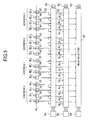
- Fig. 5 shows an essential part of a first embodiment of the present invention, and more particularly the circuit configuration of a part of a data register provided in a CPU of a one-chip microcomputer.
- the configuration shown in Fig. 5 is substituted for the conventional configuration shown in Fig. 3.
- the one-chip microcomputer according to the first embodiment of the present invention has the same block diagram as that shown in Fig. 3 except that the configurations of the data registers are different from each other.
- the data register shown in Fig. 5 includes a group of memory cells 32 - 35 specified by address 0, a group of memory cells 36 - 39 specified by address 1, a group of memory cells 44 - 47 specified by address 2, and a group of memory cells 44 - 47 specified by address 3. These memory cells are connected to a word line WL and bit lines BL1, /BL1 - BL16 and /BL16.
- the memory cells 32 - 47 have an identical SRAM circuit configuration.
- the memory 32 is shown in Fig. 6.
- the memory cell 32 includes two inverters 49 and 50 connected in a ring formation, and nMOS transistors 51 and 52 respectively serving as transfer gates.
- the word line WL is switched to the high level, and hence the nMOS transistors 51 and 52 are turned ON.
- One of the bit lines BL1 and /BL1 is switched to the high level and the other bit line is switched to the low level on the basis of the binary value of the data to be written.
- the bit lines BL1 and /BL1 are reset to the high level via loads (not shown), and the word line WL is set to the high level.
- the nMOS transistors 51 and 52 are turned ON, and the potential of the bit line BL1 is detected.
- the data register includes a write selector 53, which selects the bit lines to which the memory cells into which data is to be written, and writes the data therein.
- the data register includes an address decoder 54, which decodes the address signal supplied from the instruction decoder 9 shown in Fig. 2, and controls the selecting operation of the write selector 53.
- the data register shown in Fig. 5 includes a read selector 57, which selects the bit lines connected to the memory cells from which data is to be read, and reads the data therefrom.
- the data register includes an address decoder 58, which decodes the address signal supplied from the instruction decoder 9, and controls the selecting operation of the read selector 57.
- the data register shown in Fig. 5 includes a write bus 59 via which write data is transferred to the write selector 53, a read bus 60 via which data read via the read selector 55 is transferred, and a read bus 61 via which data read via the read selector 57 is transferred.
- Figs. 7 through 10 show segmented parts of the write selector 53.
- the data register shown in Fig. 5 includes bit line selecting lines 62 and 63 used to select bit lines BL1, /BL1, BL2, /BL2, BL3, /BL3, BL4 and /BL4, these bit lines being connected to the memory cells 32, 33, 34 and 35 having address 0.
- the data register shown in Fig. 5 includes bit line selecting lines 64 and 65 used to select bit lines BL5, /BL5, BL6, /BL6, BL7, /BL7, BL8 and /BL8, these bit lines being connected to the memory cells 36, 37, 38 and 39 having address 1.
- the data register shown in Fig. 5 includes bit line selecting lines 66 and 67 used to select bit lines BL9, /BL9, BL10, /BL10, BL11, /BL11, BL12 and /BL12, these bit lines being connected to the memory cells 40, 41, 42 and 43 having address 2.
- the data register shown in Fig. 5 includes bit line selecting lines 68 and 69 used to select bit lines BL13, /BL13, BL14, /BL14, BL15, /BL15, BL16 and /BL16, these bit lines being connected to the memory cells 44, 45, 46 and 47 having address 3.
- write buses 70 - 73 forming the write bus 59 are provided. Further, the configuration shown in Fig. 7 includes inverters 74 - 81, clocked CMOS inverters 82 - 89 of a CMOS structure with a transfer gate function. The configuration shown in Fig. 8 includes inverters 90 - 93 and clocked CMOS inverters 94 - 100. The configuration shown in Fig. 9 includes inverters 102 - 105 and clocked CMOS inverters 106 - 113. The configuration shown in Fig. 10 includes inverters 114 - 117 and clocked CMOS inverters 118 - 125.
- the read selector 55 includes bit line selecting lines 126 through 129.
- the bit line selecting line 126 is used to select the bit lines BL1, BL2, BL3 and BL4 connected to the memory cells 32, 33, 34 and 35 specified by address 0.
- the bit line selecting line 127 is used to select the bit lines BL5, BL6, BL7 and BL8 connected to the memory cells 36, 37, 38 and 39 specified by address 1.
- the bit line selecting line 128 is used to select the bit lines BL9, BL10, BL11 and BL12 connected to the memory cells 40, 41, 42 and 43 specified by address 2.
- the bit line selecting line 129 is used to select the bit lines BL13, BL14, BL15 and BL16 connected to the memory cells 44, 45, 46 and 47 specified by address 3.
- Bus lines 130 - 133 form the read bus 55.
- the read selector 55 includes NOR circuits 134 through 137 and nMOS transistors 138 - 141. As shown in Fig. 12, the read selector 55 includes NOR circuits 142 - 145 and nMOS transistors 146 - 149. As shown in Fig. 13, the read selector 55 includes NOR circuits 150 - 153 and nMOS transistors 154 - 157. As shown in Fig. 14, the read selector 55 includes NOR circuits 158 - 161 and nMOS transistors 162 - 165.
- the read selector 57 includes bit line selecting lines 166 through 169.
- the bit line selecting line 166 is used to select the bit lines BL1, BL2, BL3 and BL4 connected to the memory cells 32, 33, 34 and 35 specified by address 0.
- the bit line selecting line 167 is used to select the bit lines BL5, BL6, BL7 and BL8 connected to the memory cells 36, 37, 38 and 39 specified by address 1.
- the bit line selecting line 168 is used to select the bit lines BL9, BL10, BL11 and BL12 connected to the memory cells 40, 41, 42 and 43 specified by address 2.
- the bit line selecting line 169 is used to select the bit lines BL13, BL14, BL15 and BL16 connected to the memory cells 44, 45, 46 and 47 specified by address 3.
- Bus lines 170 - 173 form the read bus 61.
- the read selector 57 includes NOR circuits 174 through 177 and nMOS transistors 178 - 181. As shown in Fig. 16, the read selector 57 includes NOR circuits 182- 185 and nMOS transistors 186 - 189. As shown in Fig. 17, the read selector 57 includes NOR circuits 190 - 193 and nMOS transistors 194 - 197. As shown in Fig. 18, the read selector 57 includes NOR circuits 198 - 201 and nMOS transistors 202 - 205.
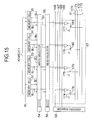
- Fig. 19 shows the operation of the write selector 53, and more particularly an operation in which the memory cells 32 - 35 specified by address 0 are selected, and high, low, high and low data values are written into the memory cells 32, 33, 34 and 35, respectively.
- reference numbers 206 - 208 indicate flip-flops
- reference numbers 209 - 214 indicate inverters
- reference numbers 215 - 220 indicate nMOS transistors.
- the word line WL is switched to the high level, and hence the nMOS transistors of the memory cells 32 - 47 serving as the transfer gates such as nMOS transistors 51, 52, 215 - 220 are turned ON.
- the bus lines 70, 71, 72 and 73 are set to the high, low, high and low levels, respectively.
- the bit line selecting lines 62, 63, 64, 65, 66, 67, 68 and 69 are set to the high, low, low, high, low, high, low and high levels, respectively.
- the clocked CMOS inverters 82 - 89 are activated, and the clocked CMOS inverters 94 - 101, 106 - 113, 118 - 125 are made inactive.
- the memory cells 32 - 35 of address 0 are selected, while the memory cells 36 - 47 of addresses 1, 2 and 3 are not selected.
- Fig. 20 shows the operation of the read selector 55, and more particularly an operation in which data are read from the memory cells 32 - 35 of address 0 via the read selector 55 in a case where data H, L, H and L are stored in the memory cells 32, 33, 34 and 35, respectively.
- reference numbers 221 - 224 denote nMOS transistors serving as loads, and symbol KB denotes a control clock signal.
- bit lines BL1, /BL1 - BL16 and /BL16 are reset to the high level via the loads, and the word line WL is switched to the high level.
- the nMOS transistors of the memory cells 32 - 35 functioning as the transfer gates, such as nMOS transistors 51, 52, 215 - 220, are turned ON.
- control clock signal KB is set to the high level, and the bus lines 130 - 133 are reset to the high level. Further, the bit line selecting line 126 is switched to the low level, and the bit line selecting lines 127 - 129 are set to the high level. As a result, the output signals of the NOR circuits 134, 135, 136 and 137 are switched to L, H, L and H, respectively. The nMOS transistors 138, 139, 140 and 141 are turned OFF, ON, OFF and ON, respectively.
- the output signals of the NOR circuits 142 - 145, 150 - 153, 158 - 161 respectively provided for the memory cells 36 - 47 are switched to the low level, and the output signals of the nMOS transistors 146 - 149, 154 - 157 and 162 - 165 are turned OFF.
- the bit lines 130, 131, 312 and 133 are set to H, L, H and L, respectively, and data stored in the memory cells 32 - 35 can be read therefrom.
- the read selector 57 operates in the same manner as the read selector 55.
- the write operation via the write selector 53 and two read operations via the read selectors 55 and 57 can be simultaneously performed under the condition that the same address is not selected.
- the write operation on the memory cells 32 - 35 specified by address 0 via the write selector 53, the first read operation on the memory cells 36 - 39 specified by address 1 via the read selector 55, and the second read operation on the memory cells 44 - 47 specified by address 3 via the read selector 57 can be simultaneously performed.
- each memory cell has two nMOS transistors functioning as transfer gates, whereby the area occupied by one memory cell can be reduced and the chip size can be diminished.
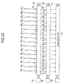
- FIG. 21 and 22 show an essential part of a data register in a CPU of a one-chip microprocessor.
- the configuration shown in Figs. 21 and 22 is substituted for the configuration shown in Fig. 3.
- the data register shown in Figs. 21 and 22 includes memory cells 225 - 228 of address 0, memory cells 229 - 232 of address 1, memory cells 233 - 236 of address 2 and memory cells 237 - 240 of address 3. Further, the data register includes memory cells 241 - 244 of address 4, memory cells 245 - 248 of address 5, memory cells 249 - 252 of address 6, and memory cells 253 - 256 of address 7. Furthermore, the data register includes memory cells 257 - 260 of address 8, memory cells 261 - 264 of address 9, memory cells 265 - 268 of address 10, and memory cells 269 - 272 of address 11.
- the data register includes a word line WL1 used to perform ON/OFF control of the transfer gates of the memory cells 225 - 240, a word line WL2 used to perform ON/OFF control of the transfer gates of the memory cells 241 - 256, and a word line WL3 used to perform ON/OFF control of the transfer gates of the memory cells 257 - 272. Further, the data register includes an address decoder 273 which selects one of the word lines WL1 - WL3, and bit lines BL1, /BL1 - BL16 and /BL16.
- the memory cells 225 - 272 have an identical structure, and has an SRAM cell structure as shown in Fig. 6.
- bit lines BL1 - /BL4 are commonly provided for the memory cells of addresses 0, 4 and 8, so that these cells are grouped (in a bank).
- the other bit lines are provided in the same manner as the bit lines BL1 - /BL4.
- the data register includes the aforementioned write selector 53, the read selector 55, the read selector 57, the address decoders 54, 56 and 58, the write bus 59, the read bus 60 and the read bus 61, these parts being used in the first embodiment of the present invention.
- the write operation via the write selector 53 and the two read operations via the read selectors 55 and 57 can be simultaneously performed under the condition that two or three of the word lines WL1 - WL3 are not concurrently selected and the same address is not selected.
- the write operation on the memory cells 225 - 228 specified by address 0 via the write selector 53, the first read operation on the memory cells 229 - 232 specified by address 1 via the read selector 55, and the second read operation on the memory cells 233 - 236 specified by address 2 via the read selector 57 can be simultaneously performed.
- the write operation on the memory cells 245 - 248 specified by address 5 via the write selector 53, the first read operation on the memory cells 249 - 252 specified by address 6 via the read selector 55, and the second read operation on the memory cells 253 - 256 specified by address 7 via the read selector 57 can be simultaneously performed.
- each memory cell two nMOS transistors functioning as transfer gates, whereby the area occupied by one memory cell can be reduced and the chip size can be diminished.
Landscapes
- Engineering & Computer Science (AREA)
- Microelectronics & Electronic Packaging (AREA)
- Static Random-Access Memory (AREA)
- Microcomputers (AREA)
Applications Claiming Priority (3)
| Application Number | Priority Date | Filing Date | Title |
|---|---|---|---|
| JP13497393 | 1993-06-04 | ||
| JP134973/93 | 1993-06-04 | ||
| JP5134973A JPH06349281A (ja) | 1993-06-04 | 1993-06-04 | 半導体装置 |
Publications (3)
| Publication Number | Publication Date |
|---|---|
| EP0627740A2 true EP0627740A2 (de) | 1994-12-07 |
| EP0627740A3 EP0627740A3 (de) | 1995-08-09 |
| EP0627740B1 EP0627740B1 (de) | 1999-08-25 |
Family
ID=15140940
Family Applications (1)
| Application Number | Title | Priority Date | Filing Date |
|---|---|---|---|
| EP94302934A Expired - Lifetime EP0627740B1 (de) | 1993-06-04 | 1994-04-25 | Datenregisterstruktur und integrierte Halbleiteranordnung mit einer solchen Struktur |
Country Status (4)
| Country | Link |
|---|---|
| US (1) | US5606525A (de) |
| EP (1) | EP0627740B1 (de) |
| JP (1) | JPH06349281A (de) |
| DE (1) | DE69420189T2 (de) |
Families Citing this family (3)
| Publication number | Priority date | Publication date | Assignee | Title |
|---|---|---|---|---|
| TW330265B (en) * | 1994-11-22 | 1998-04-21 | Hitachi Ltd | Semiconductor apparatus |
| US6366502B1 (en) * | 2000-06-05 | 2002-04-02 | Stmicroelectronics Limited | Circuitry for reading from and writing to memory cells |
| US20050245364A1 (en) * | 2004-04-30 | 2005-11-03 | Juliu Horvath | Exercise device |
Family Cites Families (10)
| Publication number | Priority date | Publication date | Assignee | Title |
|---|---|---|---|---|
| US3968480A (en) * | 1974-04-25 | 1976-07-06 | Honeywell Inc. | Memory cell |
| FR2493641A1 (fr) * | 1980-11-03 | 1982-05-07 | Efcis | Reseau logique integre a programmation electrique simplifiee |
| US4488264A (en) * | 1982-06-10 | 1984-12-11 | Dshkhunian Valery | Transistor storage |
| JPS62287497A (ja) * | 1986-06-06 | 1987-12-14 | Fujitsu Ltd | 半導体記憶装置 |
| EP0258715B1 (de) * | 1986-08-15 | 1994-06-08 | Nec Corporation | Statischer Direktzugriffspeicher einer Bi-CMOS-Konstruktion |
| US5287485A (en) * | 1988-12-22 | 1994-02-15 | Digital Equipment Corporation | Digital processing system including plural memory devices and data transfer circuitry |
| US5226142A (en) * | 1990-11-21 | 1993-07-06 | Ross Technology, Inc. | High performance register file with overlapping windows |
| JP2601951B2 (ja) * | 1991-01-11 | 1997-04-23 | 株式会社東芝 | 半導体集積回路 |
| JP3481263B2 (ja) * | 1992-02-19 | 2003-12-22 | 株式会社リコー | シリアル記憶装置 |
| JPH05274879A (ja) * | 1992-03-26 | 1993-10-22 | Nec Corp | 半導体装置 |
-
1993
- 1993-06-04 JP JP5134973A patent/JPH06349281A/ja active Pending
-
1994
- 1994-04-25 EP EP94302934A patent/EP0627740B1/de not_active Expired - Lifetime
- 1994-04-25 DE DE69420189T patent/DE69420189T2/de not_active Expired - Fee Related
-
1995
- 1995-11-09 US US08/552,459 patent/US5606525A/en not_active Expired - Fee Related
Also Published As
| Publication number | Publication date |
|---|---|
| DE69420189D1 (de) | 1999-09-30 |
| DE69420189T2 (de) | 1999-12-09 |
| EP0627740B1 (de) | 1999-08-25 |
| US5606525A (en) | 1997-02-25 |
| EP0627740A3 (de) | 1995-08-09 |
| JPH06349281A (ja) | 1994-12-22 |
Similar Documents
| Publication | Publication Date | Title |
|---|---|---|
| US5036486A (en) | Associative memory device | |
| US5325501A (en) | Associative memory | |
| US8117567B2 (en) | Structure for implementing memory array device with built in computation capability | |
| US5319763A (en) | Data processor with concurrent static and dynamic masking of operand information and method therefor | |
| US4153933A (en) | Single chip MOS computer with expandable memory | |
| JP3562552B2 (ja) | メモリ用マルチ・スレッド・セル | |
| GB1527316A (en) | Data processing apparatus | |
| US3644906A (en) | Hybrid associative memory | |
| US4037094A (en) | Multi-functional arithmetic and logical unit | |
| US4179738A (en) | Programmable control latch mechanism for a data processing system | |
| US4028682A (en) | Circuit arrangement for selecting the function of connection contacts on circuit chips | |
| EP0145497A2 (de) | Integrierte Halbleiterschaltungsanordnung | |
| EP0408353B1 (de) | Integrierte Halbleiterschaltung | |
| EP0230668B1 (de) | Arithmetisch-logische Schaltung | |
| US6834024B2 (en) | Reduced size multi-port register cell | |
| JPH09120693A (ja) | 半導体記憶装置 | |
| WO1984003377A1 (en) | A cmos multiport general purpose register | |
| US5220526A (en) | Method and apparatus for indicating a duplication of entries in a content addressable storage device | |
| EP0627740B1 (de) | Datenregisterstruktur und integrierte Halbleiteranordnung mit einer solchen Struktur | |
| US4811266A (en) | Multifunction arithmetic indicator | |
| US5101376A (en) | Integrated microprocessor with associative memory device | |
| US5664156A (en) | Microcontroller with a reconfigurable program status word | |
| US3432810A (en) | Addressing system for a computer employing a plurality of local storage units in addition to a main memory | |
| US3962684A (en) | Computing system interface using common parallel bus and segmented addressing | |
| US5606709A (en) | Register group circuit for data processing system |
Legal Events
| Date | Code | Title | Description |
|---|---|---|---|
| PUAI | Public reference made under article 153(3) epc to a published international application that has entered the european phase |
Free format text: ORIGINAL CODE: 0009012 |
|
| AK | Designated contracting states |
Kind code of ref document: A2 Designated state(s): DE FR GB |
|
| PUAL | Search report despatched |
Free format text: ORIGINAL CODE: 0009013 |
|
| AK | Designated contracting states |
Kind code of ref document: A3 Designated state(s): DE FR GB |
|
| 17P | Request for examination filed |
Effective date: 19960201 |
|
| 17Q | First examination report despatched |
Effective date: 19980323 |
|
| GRAG | Despatch of communication of intention to grant |
Free format text: ORIGINAL CODE: EPIDOS AGRA |
|
| GRAG | Despatch of communication of intention to grant |
Free format text: ORIGINAL CODE: EPIDOS AGRA |
|
| GRAH | Despatch of communication of intention to grant a patent |
Free format text: ORIGINAL CODE: EPIDOS IGRA |
|
| GRAH | Despatch of communication of intention to grant a patent |
Free format text: ORIGINAL CODE: EPIDOS IGRA |
|
| GRAA | (expected) grant |
Free format text: ORIGINAL CODE: 0009210 |
|
| AK | Designated contracting states |
Kind code of ref document: B1 Designated state(s): DE FR GB |
|
| REF | Corresponds to: |
Ref document number: 69420189 Country of ref document: DE Date of ref document: 19990930 |
|
| ET | Fr: translation filed | ||
| PLBE | No opposition filed within time limit |
Free format text: ORIGINAL CODE: 0009261 |
|
| STAA | Information on the status of an ep patent application or granted ep patent |
Free format text: STATUS: NO OPPOSITION FILED WITHIN TIME LIMIT |
|
| 26N | No opposition filed | ||
| REG | Reference to a national code |
Ref country code: GB Ref legal event code: IF02 |
|
| PGFP | Annual fee paid to national office [announced via postgrant information from national office to epo] |
Ref country code: FR Payment date: 20040408 Year of fee payment: 11 |
|
| PGFP | Annual fee paid to national office [announced via postgrant information from national office to epo] |
Ref country code: GB Payment date: 20040421 Year of fee payment: 11 |
|
| PGFP | Annual fee paid to national office [announced via postgrant information from national office to epo] |
Ref country code: DE Payment date: 20040506 Year of fee payment: 11 |
|
| PG25 | Lapsed in a contracting state [announced via postgrant information from national office to epo] |
Ref country code: GB Free format text: LAPSE BECAUSE OF NON-PAYMENT OF DUE FEES Effective date: 20050425 |
|
| PG25 | Lapsed in a contracting state [announced via postgrant information from national office to epo] |
Ref country code: DE Free format text: LAPSE BECAUSE OF NON-PAYMENT OF DUE FEES Effective date: 20051101 |
|
| GBPC | Gb: european patent ceased through non-payment of renewal fee |
Effective date: 20050425 |
|
| PG25 | Lapsed in a contracting state [announced via postgrant information from national office to epo] |
Ref country code: FR Free format text: LAPSE BECAUSE OF NON-PAYMENT OF DUE FEES Effective date: 20051230 |
|
| REG | Reference to a national code |
Ref country code: FR Ref legal event code: ST Effective date: 20051230 |