EP0623964A2 - Fangstellen benutzende Halbleiterbauelemente - Google Patents
Fangstellen benutzende Halbleiterbauelemente Download PDFInfo
- Publication number
- EP0623964A2 EP0623964A2 EP94300140A EP94300140A EP0623964A2 EP 0623964 A2 EP0623964 A2 EP 0623964A2 EP 94300140 A EP94300140 A EP 94300140A EP 94300140 A EP94300140 A EP 94300140A EP 0623964 A2 EP0623964 A2 EP 0623964A2
- Authority
- EP
- European Patent Office
- Prior art keywords
- semiconductor device
- damaging
- trap sites
- creating
- semiconductor
- Prior art date
- Legal status (The legal status is an assumption and is not a legal conclusion. Google has not performed a legal analysis and makes no representation as to the accuracy of the status listed.)
- Withdrawn
Links
Images


Classifications
-
- H—ELECTRICITY
- H10—SEMICONDUCTOR DEVICES; ELECTRIC SOLID-STATE DEVICES NOT OTHERWISE PROVIDED FOR
- H10D—INORGANIC ELECTRIC SEMICONDUCTOR DEVICES
- H10D30/00—Field-effect transistors [FET]
- H10D30/60—Insulated-gate field-effect transistors [IGFET]
- H10D30/69—IGFETs having charge trapping gate insulators, e.g. MNOS transistors
-
- H—ELECTRICITY
- H10—SEMICONDUCTOR DEVICES; ELECTRIC SOLID-STATE DEVICES NOT OTHERWISE PROVIDED FOR
- H10B—ELECTRONIC MEMORY DEVICES
- H10B69/00—Erasable-and-programmable ROM [EPROM] devices not provided for in groups H10B41/00 - H10B63/00, e.g. ultraviolet erasable-and-programmable ROM [UVEPROM] devices
-
- H—ELECTRICITY
- H10—SEMICONDUCTOR DEVICES; ELECTRIC SOLID-STATE DEVICES NOT OTHERWISE PROVIDED FOR
- H10D—INORGANIC ELECTRIC SEMICONDUCTOR DEVICES
- H10D62/00—Semiconductor bodies, or regions thereof, of devices having potential barriers
- H10D62/50—Physical imperfections
- H10D62/57—Physical imperfections the imperfections being on the surface of the semiconductor body, e.g. the body having a roughened surface
-
- H10P36/03—
Definitions
- the present invention relates generally to semiconductor devices, and more particularly, to semiconductor devices that intentionally employ traps and methods for fabricating such semiconductor devices.
- Hot electrons are electrons which have sufficient energy to travel through oxides and the silicon substrate thereby damaging the material through which it travels. When these energetic electrons damage the materials in a transistor (or other semiconductor device) or become trapped in the gate oxide, the transistor (or semiconductor device) parameters are changed.
- Hot holes result from the interaction of the mobile electrons in the material, or from the generation of hot electrons (current in opposite directions), with imperfections in the substrate or imperfections at the oxide/substrate interface. Such imperfections require the least energy for hot hole/electrons to change the transistor or semiconductor device characteristics, i.e., Vt.
- Vt the transistor or semiconductor device
- transistor structures are built in such a way that the junction is not abrupt. That is, the doping level of the junction changes as it approaches the gate edge of a transistor.
- a transistor with a graded junction is said to have a lightly doped drain (LDD) configuration.
- LDD lightly doped drain
- the transistor is formed. That is, a polysilicon gate oxide stack is formed over the silicon substrate. Typically, an implant is done after this step to provide a light dopant level next to the gate edge which in subsequent heating steps will be driven in under the gate edge to make electrical contact with the electrically active area of the gate.
- a sidewall oxide is formed as a spacer to force the subsequent implants away from the gate edge.
- a heavy dopant level is implanted in the substrate to form the conductive region called a moat.
- the heavily implanted region may have more than one dopant with different diffusion constants to further grade the junction.
- the implanted dopants in the moat diffuse under the sidewall oxide to complete the electrical connection to the gate.
- the substrate must be free from defects known as trap sites, or the sites must be neutralized by the addition of hydrogen in the substrate. The hydrogen binds to the trap sites rendering them electrically inactive.
- semiconductor devices are provided that intentionally employ trap sites, either in the substrate (at or near the face of the substrate) or in silicon dioxide or other semiconductor/dielectric layers located above the substrate.
- methods are provided for fabricating such semiconductor devices.
- the simplest semiconductor device of the present invention is a semiconductor device having an implanted region defined in the face of a body of semiconductor material and having a plurality of traps in a portion of this implanted region (also at or near the face of the semiconductor).
- a conductive layer (of semiconductor or metal) insulatingly abuts this implanted region and also abuts the plurality of traps.
- the conductive layer may be used to provide varying strength electric fields to influence the interaction of charged carriers of current in the implanted region with the traps at the face of the semiconductor and thereby adjust the resistance of the implanted region, which may be, for example, a bus or bit line.
- Such a device is an edge-effect semiconductor device.
- the conductive layer may be extended to insulatingly overlay the implanted region and traps.
- an insulated gate field effect transistor device having source and drain regions defined in the face of a body of a semiconductor material and has a channel region therebetween. A plurality of traps are located at or near the face of the semiconductor in this channel region. A gate conductor, between the source and drain, is located near the face of the semiconductor over the channel but is insulated from the semiconductor by a gate insulator. The gate insulator and/or any sidewall oxide may also optionally contain trap sites at or near its interface with the body of semiconductor material. Such an insulated gate field-effect transistor device that intentionally employs a plurality of traps may be used as an electrically programmable memory device.
- additional layers of gate insulating material and conductors may be "stacked" upon the first gate structure to provide alternative structures also suitable for electrically programmable memory devices.
- trap sites may also be optionally located in any gate oxide or other dielectric layer located at or above the face of the semiconductor material.
- sidewall oxides may be added to the sides of the initial gate. The sidewall oxides may optionally have traps at their interfaces with the substrate.
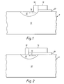
- FIG. 1 there may be seen a cross-sectional view of an edge-effect semiconductor device 8 of the present invention. More particularly, it may be seen that there is a substrate of semiconductor material 10 in which there is an implanted region 12 that defines a "bus", a bit bar, or other line for allowing current to be passed from one area of the semiconductor substrate to a different area.
- a series of traps or trap sites 14, denoted by the "plus” signs located at or near the face of the semiconductor in a portion of the implanted region 12.
- These traps 14, as noted later herein, are preferably formed either by implantation (using one or more different ions) or by an etching technique.
- implantation and etching techniques may cause surface imperfections or traps.
- the present invention takes advantage of these known implantation or etching techniques to provide a suitable number of trap sites at or near the surface of the semiconductor device. It is currently believed that tens to hundreds, of such trap sites may be employed to controllably alter the operating characteristics of a semiconductor device. Such operative trap sites, regardless of their actual numbers, are referred to herein as a "plurality" of trap sites.
- Figure 1 depicts a conductive layer 16 abutting a portion of the implanted region 12 that contains the traps 14.
- An optional sidewall oxide 18 is also shown, and may overlay a portion of the layer 16, but is only depicted overlaying a portion of the implanted region 12 and trap region 14.
- the conductive layer 16 is insulated from the substrate 10 by a dielectric layer 20, which may be a silicon dioxide layer. In this manner, the electric field generated by the conductive layer 16, which typically is polysilicon, will influence the charge carriers of current that are traveling through or along the implanted region 12 causing the trap site 14 fill density to be altered.
- region 12 in combination with the insulated conductive layer 16 may be characterized as a controllable analogue voltage source, or a line variable resistance.
- a line variable resistance may be employed to alter a circuit's RC constant and thereby alter the operating characteristics of such a circuit.
- the optional sidewall oxide 18 of Figure 1 allows for more dispersion of the electric field to provide a broader scope of coverage over the implanted region 12 and accordingly cause more charge carriers of current to interact with the trap sites 14 located in the implanted region 12, and accordingly provide more control over the variation of the resistance characteristics of this implanted region 12 to these charge carriers.
- the sidewall oxide may also contain trap sites (not depicted in Figure 1 for ease of illustration purposes).
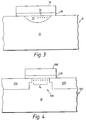
- the conductive layer 16 of Figure 1 may be continued, to insulatingly extend (as depicted in Figure 2) over some, substantially all, or (as depicted in Figure 3) all, of the implanted region 12.
- the conductive layer 16 may be adjacent (either abut or overlay) the implanted region 12.
- additional implant regions may be provided on either side of the layer to allow for the formation of an insulated gate field-effect transistor device.
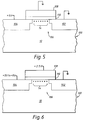
- FIG. 4 there may be seen a simplified cross-sectional depiction of such an insulated gate field-effect transistor semiconductor device 100. More particularly, it may be seen that there are source 102 and drain 104 regions defined in the face of a body of a semiconductor material 10 and that there is a channel 106 between the source 102 and the drain 104 regions. There are a plurality of traps 14 at or near the face of the semiconductor in this channel region 106.
- a gate 108 is depicted as extending between the source 102 and drain 104 regions on top of the face of the semiconductor 10 and this gate 108 covers this channel region 106 and is insulated from the semiconductor material by an appropriate gate insulator or dielectric 110.
- the gate 108 and dielectric 110 are analogous to the conductive layer 16 and dielectric 20, of Figures 1, 2 and 3.
- the gate conductor 108 is preferably a polysilicon layer.
- trap sites 14 may also optionally be located in the gate dielectric layer, 110 at or near its interface with the substrate.
- silicon dioxide is employed as a dielectric layer 110, but other layers may be so employed, such as, for example, but not limited to silicon nitride, or sandwiched layers of silicon nitride and dioxide.
- trap sites may be employed in other circuit technologies, such as bipolar, to affect operating characteristics of transistors and other semiconductor devices.
- bipolar the traps are at the collector and emitter terminals and not "in” the transistor structure. These traps then alter the resistance at these terminals to affect the transistor's operation.
- the present invention deliberately employs trap sites 14 in a portion of semiconductor material 10 or layers 110 associated therewith to alter the operating characteristics of semiconductor devices. That is, the present invention takes advantage of and utilizes any hot carriers (electrons or holes) and their interactions with trap sites.
- the present invention intentionally uses trap sites 14 in the area of the substrate 10 under the gate oxide 110, and optionally under any sidewall oxide, to create a memory device where the data state can be changed electrically and the retention of the data state is on the order of days to years.
- no refresh circuit is required, and no extra voltage levels are required beyond the normal operating voltage of the device 100, as described more fully later herein.
- a preferred embodiment of the present invention is a memory device, such as an EPROM.
- the EPROM 100 of the present invention is simpler to fabricate than conventional EPROMS, because it preferably has only a single gate structure, and is simpler to operate than conventional EPROMS.
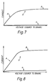
- the biasing conditions for the operation of the device 100 as an NMOS EPROM is depicted in Figures 4 and 5.
- Figure 4 depicts a "read” of the NMOS EPROM device
- Figure 5 depicts a "write" to the NMOS EPROM device.
- a "write" operation may be seen.
- the gate 108 is held at approximately a positive 2.5 volts while a voltage of 5 to 9 volts is applied across the drain 104 and source 102.
- This biasing condition causes current flow under the gate dielectric 110 and positions charges at the dielectric/substrate interface that remain after the bias is removed. These charges prevent current flow during a subsequent read operation.
- the biasing condition is held for a few tenths of a second to about one second, depending on the magnitude of the source 104 to drain 102 voltage. That is, for about 9 volts, the condition is held for about one tenth of a second, while for about 5 volts, the condition is held for about one second.
- NMOS EPROM device 100 of the present invention may employ normal MOS operating voltages, and does not require special higher voltages for reads and/or writes.
- operating curve a shows the current from drain 104 to source 102 to be 0 amperes for 0 volts gate bias.
- a gate voltage above 0 volts there exists a portion A of the curve b where the transistor is not in saturation.
- the slope of the portion A is determined by the resistance of the transistor.
- portion B of curve b indicates saturation.
- the voltage at which the transistor saturates is dependent upon the size of the transistor, the mobile ion concentration, and the resistance of the transistor.
- FIG. 8 typical operating curves a, b for an NMOS insulated gate field-effect transistor employing traps 14 is depicted.
- the slope of the portion A of curve a may be controlled by how many traps are activated.
- the NMOS transistor is now in depletion mode.
- An optional trap area in or under a sidewall may further modify the resistance of the transistor to modify the slope of region A.
- FIG 9 there may be seen an enlarged portion of a tunnelling electron microscope picture of damaged silicon in the diffusion area located under the sidewall oxide of an insulated gate field-effect transistor.
- the damaged silicon appears as a granular looking area and represents those areas of silicon which contain trap sites.
- the gate silicon dioxide, polysilicon layer, and sidewall oxide, as well as the substrate, are also shown.
- Figure 9 also contains various artifacts and interference fringes.
- such a memory device may be "unprogrammed” by exposing the device to ultraviolet (uv) radiation (or other high energy photons, such as x-rays) or by "annealing" the device at temperatures above approximately 400° C for at least one hour.
- uv ultraviolet
- x-rays other high energy photons
- FIG. 10 there may be seen a cross-sectional depiction of an insulated gate field-effect transistor semiconductor device 200 that includes sidewall oxides.
- the sidewall oxide 202 optionally, may, or may not, have in the substrate 10, or in the oxide 202, at the oxide-substrate interface, electrically active trap sites 206, 204, respectively. If traps 206 are intentionally allowed to exist under the sidewall oxide 202 in the substrate 10, they are used to modify the gain of the transistor 200. More particularly, the traps in or under 204, 206 the sidewall oxide 202 effectively add additional "resistance" to the overall transistor 200 resistance and thereby lower the gain of the transistor 200.
- the charge state of the traps may only be modified by either thermal energy or photons, such as light or x-rays, as noted earlier herein. Potentially, a reverse current through an interface having trap sites may help change the state of the charge at that interface.
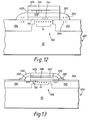
- the transistor structure of Figures 4, 5 and 6 may be modified by adding a programming gate structure over the first gate structure to provide the semiconductor device 300 depicted in Figure 11.
- This structure is similar to that used in a stacked EPROM cell.
- traps 14a are depicted in dielectric layer 110.
- traps may also be disposed in the upper dielectric layer 302, if desired.
- the structure of the transistor depicted in Figure 10 may be similarly modified to provide the semiconductor device 400 depicted in Figure 12 by also adding a programming gate structure 402, 404 over the first gate structure 108, 110.
- traps 14a, 14b may be located in either or both of dielectric layers 110, 402, respectively, as well as in or below the sidewall oxide 204, 206, respectively.
- conductive material 502 may be placed over the sidewall oxide 202 area of the transistor of Figure 12 to provide semiconductor device 500.
- the addition of this extra material 502 acts like another gate. In this way, the charge at the interface between the sidewall 202 and the substrate 10 may be appropriately controlled. More particularly, this in effect places two transistors along side and next to the "center" transistor having the double gate structure.
- An additional dielectric layer 504 insulates the conductive layer 502 from the substrate 10.
- a dielectric wedge or layer may also insulate layer 502 from layer 404.
- Dielectric layer 504 may be a continuation of sidewall oxide 202.
- conductive layer 502 may be a continuation of conductive layer 404.
- trap sites may be located in layer 110 and/or layer 402 and/or in or under the sidewall oxide 202.
- a metal covering for the entire structure of the semiconductor device of the present invention may be used as a diffusion block for any hydrogen which is diffused into the substrate to control junction leakage in transistors which are to be of high quality, have no junction leakage, have no hot carrier effects and be stable over time. That is, a guard ring may be placed around the semiconductor device of the present invention (that deliberately employs trap sites) and a suitable metal covering placed over that guard ring whenever the remaining devices on the substrate are hydrogen annealed to eliminate traps.
- the semiconductor devices of the present invention are fabricated near the end of the production process to avoid unnecessary thermal and/or annealing cycles.
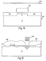
- FIG 14 there may be seen a device 600 that employs a metal layer 602 spaced from the substrate 10 and gate structure 606 by a spacer ring or layer (not depicted in Figure 14 for ease of illustration purposes).
- the gate structure 606 may be any one of the structures depicted in Figures 4, 5 and 6, or Figures 10-13.
- the metal layer 602 covers the entire device 600 structure and acts as a diffusion block for any hydrogen diffused into the chip to control junction leakage in transistors not employing trap sites.
- Any means of leaving traps on or near the surface of a semiconductor material or in a layer will provide sufficient traps to control the gate charge.
- Typical means of generating traps would be to ion implant at high energies, e.g., 120 KeV or greater, and ion implantation with large atoms such as arsenic or larger. High energy x-rays may also be employed.
- Figure 15 depicts such an ion implantation step.
- the arrows 800 depict the ions bombarding the exposed face of substrate 10 to create the trap sites 14.
- the remainder of the device on the substrate 10 is blanketed by an appropriate layer 802, such as photoresist or a low temperature layer (such as from a TEOS process) to prevent any ion damage, except for the "window" in this layer 802 where the device of the present invention will be located.
- the device of the present invention is then fabricated over this face with its active trap sites by known techniques. From wafer start to the first and/or second gate level, fabrication would follow standard process flows, for both the conventional devices blanketed by layer 802 and the devices of the present invention after trap site formation.
- ion implantation with iron or other atoms which have donor electron or hole states may also be employed. Implanting with iron is typically not done on CMOS devices because the extra states cause leakage at the junctions.
- Another way to fabricate trap sites is to plasma etch the substrate in a mode which roughens the substrate.
- One such mode is a reactive ion etch (RIE) for which the device is on the plate to which RF power is applied, gas pressures are low (less than about 300 milliTorr) and powers are high (greater than about 5 watts/in2).
- RIE reactive ion etch
- Other alternate ways to generate trap sites would be to employ a well-masked x-ray beam or an ion beam mill.
- Thermal oxide gates may be employed, but the effects of the intentional traps must not be removed.
- low temperature tetraethyl orthosilicate (TEOS) oxide gates may be used instead of the normal thermal oxide gate.
- TEOS gates may be structured to have a normal thermal oxide on top of the TEOS.
- the TEOS gate may be structured to have a nitride over the top of its gate.
- any anneal processes for semiconductor devices with intentional traps should be brief. Specifically, flash-lamp anneals (10 seconds or less), laser-scanned anneals, or low-temperature (less than 900°C) anneals for brief times (less than 30-minutes) will prevent the traps from being annealed out. Further, any hydrogen introduced into the device to stabilize the non-trapped transistors should not be allowed to diffuse into the region of any devices that employ trap cells. To prevent this, metal can be employed to inhibit the diffusion of hydrogen into the substrate. Alternatively, thick pads of semiconductor, such as for example, silicon nitride, may be employed; the thickness should be sufficient to inhibit diffusion of hydrogen therethrough during the time of the "annealing" step. A guard ring should be placed around the area of the semiconductor device employing the techniques of the present invention and should be potentially electrically active at the time of any hydrogen diffusion.
- the insulated gate field-effect transistor device of the present invention may be employed as an electrically programmable memory device, i.e., an EPROM cell.
- the semiconductor devices of the present invention may be employed as analog memory devices. That is, these memory devices may have any value or state between (and including) off to fully programmed.
- the devices of the present invention may be used as an analog current supply for analog logic in a microprocessor.
- a true neural network memory cell for use with "fuzzy" logic may also be fabricated according to the teachings of the present invention.
Landscapes
- Non-Volatile Memory (AREA)
- Insulated Gate Type Field-Effect Transistor (AREA)
- Bipolar Transistors (AREA)
- Semiconductor Integrated Circuits (AREA)
- Semiconductor Memories (AREA)
Applications Claiming Priority (2)
| Application Number | Priority Date | Filing Date | Title |
|---|---|---|---|
| US230493A | 1993-01-08 | 1993-01-08 | |
| US2304 | 1993-01-08 |
Publications (2)
| Publication Number | Publication Date |
|---|---|
| EP0623964A2 true EP0623964A2 (de) | 1994-11-09 |
| EP0623964A3 EP0623964A3 (de) | 1998-05-13 |
Family
ID=21700156
Family Applications (1)
| Application Number | Title | Priority Date | Filing Date |
|---|---|---|---|
| EP94300140A Withdrawn EP0623964A3 (de) | 1993-01-08 | 1994-01-10 | Fangstellen benutzende Halbleiterbauelemente |
Country Status (2)
| Country | Link |
|---|---|
| EP (1) | EP0623964A3 (de) |
| JP (1) | JPH06318695A (de) |
Cited By (1)
| Publication number | Priority date | Publication date | Assignee | Title |
|---|---|---|---|---|
| US7598559B2 (en) | 2005-03-04 | 2009-10-06 | Sharp Kabushiki Kaisha | Semiconductor storage device, manufacturing method therefor, and portable electronic equipment |
Families Citing this family (1)
| Publication number | Priority date | Publication date | Assignee | Title |
|---|---|---|---|---|
| JP2006237423A (ja) * | 2005-02-28 | 2006-09-07 | Oki Electric Ind Co Ltd | 半導体記憶装置および半導体記憶装置の製造方法 |
Family Cites Families (3)
| Publication number | Priority date | Publication date | Assignee | Title |
|---|---|---|---|---|
| USRE31083E (en) * | 1979-02-15 | 1982-11-16 | International Business Machines Corporation | Non-volatile memory devices fabricated from graded or stepped energy band gap insulator MIM or MIS structure |
| CA1276314C (en) * | 1988-03-24 | 1990-11-13 | Alexander Kalnitsky | Silicon ion implanted semiconductor device |
| US5065132A (en) * | 1990-11-16 | 1991-11-12 | Texas Instruments Incorporated | Programmable resistor and an array of the same |
-
1994
- 1994-01-07 JP JP6000437A patent/JPH06318695A/ja active Pending
- 1994-01-10 EP EP94300140A patent/EP0623964A3/de not_active Withdrawn
Cited By (1)
| Publication number | Priority date | Publication date | Assignee | Title |
|---|---|---|---|---|
| US7598559B2 (en) | 2005-03-04 | 2009-10-06 | Sharp Kabushiki Kaisha | Semiconductor storage device, manufacturing method therefor, and portable electronic equipment |
Also Published As
| Publication number | Publication date |
|---|---|
| JPH06318695A (ja) | 1994-11-15 |
| EP0623964A3 (de) | 1998-05-13 |
Similar Documents
| Publication | Publication Date | Title |
|---|---|---|
| US6479866B1 (en) | SOI device with self-aligned selective damage implant, and method | |
| US6580149B2 (en) | Double LDD devices for improved DRAM refresh | |
| US7560368B2 (en) | Insulated gate planar integrated power device with co-integrated Schottky diode and process | |
| US7348243B2 (en) | Semiconductor device and method for fabricating the same | |
| US5527724A (en) | Method to prevent latch-up and improve breakdown volatge in SOI mosfets | |
| US6444548B2 (en) | Bitline diffusion with halo for improved array threshold voltage control | |
| US6358783B1 (en) | Semiconductor device and method of manufacturing the same | |
| US6963108B1 (en) | Recessed channel | |
| US6744105B1 (en) | Memory array having shallow bit line with silicide contact portion and method of formation | |
| US20050233506A1 (en) | Semiconductor device with leakage implant and method of fabrication | |
| US4637128A (en) | Method of producing semiconductor device | |
| US6306737B1 (en) | Method to reduce source-line resistance in flash memory with sti | |
| US5386133A (en) | LDD FET with polysilicon sidewalls | |
| US6218251B1 (en) | Asymmetrical IGFET devices with spacers formed by HDP techniques | |
| JP3549364B2 (ja) | 三重ウェルを有するフラッシュ・メモリ・セルの製造方法 | |
| US5627087A (en) | Process for fabricating metal-oxide semiconductor (MOS) transistors based on lightly doped drain (LDD) structure | |
| US5397727A (en) | Method of forming a floating gate programmable read only memory cell transistor | |
| US8664706B2 (en) | Current in one-time-programmable memory cells | |
| US5874343A (en) | CMOS integrated circuit and method for forming source/drain areas prior to forming lightly doped drains to optimize the thermal diffusivity thereof | |
| US5677215A (en) | Method of fabricating a nonvolatile semiconductor memory device | |
| US5477072A (en) | Nonvolatile semiconductor memory device | |
| JPH0210775A (ja) | イオン注入半導体デバイス | |
| EP0623964A2 (de) | Fangstellen benutzende Halbleiterbauelemente | |
| US6538284B1 (en) | SOI device with body recombination region, and method | |
| WO2006033717A2 (en) | Non-volatile nanocrystal memory transistors using low voltage impact ionization |
Legal Events
| Date | Code | Title | Description |
|---|---|---|---|
| PUAI | Public reference made under article 153(3) epc to a published international application that has entered the european phase |
Free format text: ORIGINAL CODE: 0009012 |
|
| AK | Designated contracting states |
Kind code of ref document: A2 Designated state(s): DE FR GB IT NL |
|
| PUAL | Search report despatched |
Free format text: ORIGINAL CODE: 0009013 |
|
| AK | Designated contracting states |
Kind code of ref document: A3 Designated state(s): DE FR GB IT NL |
|
| 17P | Request for examination filed |
Effective date: 19981113 |
|
| STAA | Information on the status of an ep patent application or granted ep patent |
Free format text: STATUS: THE APPLICATION IS DEEMED TO BE WITHDRAWN |
|
| 18D | Application deemed to be withdrawn |
Effective date: 19990803 |