EP0623932A2 - Soft error immune CMOS static RAM cell - Google Patents
Soft error immune CMOS static RAM cell Download PDFInfo
- Publication number
- EP0623932A2 EP0623932A2 EP94480022A EP94480022A EP0623932A2 EP 0623932 A2 EP0623932 A2 EP 0623932A2 EP 94480022 A EP94480022 A EP 94480022A EP 94480022 A EP94480022 A EP 94480022A EP 0623932 A2 EP0623932 A2 EP 0623932A2
- Authority
- EP
- European Patent Office
- Prior art keywords
- memory cell
- transistors
- recited
- well
- conductivity type
- Prior art date
- Legal status (The legal status is an assumption and is not a legal conclusion. Google has not performed a legal analysis and makes no representation as to the accuracy of the status listed.)
- Withdrawn
Links
- 230000003068 static effect Effects 0.000 title description 6
- 230000015654 memory Effects 0.000 claims abstract description 68
- 239000000758 substrate Substances 0.000 claims abstract description 23
- 238000002955 isolation Methods 0.000 claims abstract description 10
- 239000004065 semiconductor Substances 0.000 claims description 9
- 230000005669 field effect Effects 0.000 claims description 5
- 239000000463 material Substances 0.000 claims description 2
- 230000000295 complement effect Effects 0.000 claims 2
- 229910044991 metal oxide Inorganic materials 0.000 claims 1
- 150000004706 metal oxides Chemical class 0.000 claims 1
- 210000004027 cell Anatomy 0.000 abstract description 60
- 239000002245 particle Substances 0.000 abstract description 11
- 230000036039 immunity Effects 0.000 abstract description 5
- 230000005865 ionizing radiation Effects 0.000 abstract description 4
- 230000015572 biosynthetic process Effects 0.000 abstract description 3
- 210000000352 storage cell Anatomy 0.000 abstract description 3
- 230000009467 reduction Effects 0.000 description 7
- 238000010586 diagram Methods 0.000 description 6
- 238000004519 manufacturing process Methods 0.000 description 5
- 238000009792 diffusion process Methods 0.000 description 3
- 230000010354 integration Effects 0.000 description 3
- 238000012545 processing Methods 0.000 description 3
- 230000008859 change Effects 0.000 description 2
- 239000004020 conductor Substances 0.000 description 2
- 238000011161 development Methods 0.000 description 2
- 238000005516 engineering process Methods 0.000 description 2
- 230000006872 improvement Effects 0.000 description 2
- 230000007246 mechanism Effects 0.000 description 2
- 238000000034 method Methods 0.000 description 2
- 230000002093 peripheral effect Effects 0.000 description 2
- 238000000926 separation method Methods 0.000 description 2
- LBDSXVIYZYSRII-IGMARMGPSA-N alpha-particle Chemical compound [4He+2] LBDSXVIYZYSRII-IGMARMGPSA-N 0.000 description 1
- 239000003990 capacitor Substances 0.000 description 1
- 238000006880 cross-coupling reaction Methods 0.000 description 1
- 230000007547 defect Effects 0.000 description 1
- 238000013461 design Methods 0.000 description 1
- 238000007599 discharging Methods 0.000 description 1
- 239000003574 free electron Substances 0.000 description 1
- 239000012535 impurity Substances 0.000 description 1
- 239000012212 insulator Substances 0.000 description 1
- 230000005012 migration Effects 0.000 description 1
- 238000013508 migration Methods 0.000 description 1
- 230000003071 parasitic effect Effects 0.000 description 1
- 230000000737 periodic effect Effects 0.000 description 1
- 230000004044 response Effects 0.000 description 1
- 230000002441 reversible effect Effects 0.000 description 1
Images

Classifications
-
- H—ELECTRICITY
- H10—SEMICONDUCTOR DEVICES; ELECTRIC SOLID-STATE DEVICES NOT OTHERWISE PROVIDED FOR
- H10B—ELECTRONIC MEMORY DEVICES
- H10B10/00—Static random access memory [SRAM] devices
- H10B10/12—Static random access memory [SRAM] devices comprising a MOSFET load element
-
- Y—GENERAL TAGGING OF NEW TECHNOLOGICAL DEVELOPMENTS; GENERAL TAGGING OF CROSS-SECTIONAL TECHNOLOGIES SPANNING OVER SEVERAL SECTIONS OF THE IPC; TECHNICAL SUBJECTS COVERED BY FORMER USPC CROSS-REFERENCE ART COLLECTIONS [XRACs] AND DIGESTS
- Y10—TECHNICAL SUBJECTS COVERED BY FORMER USPC
- Y10S—TECHNICAL SUBJECTS COVERED BY FORMER USPC CROSS-REFERENCE ART COLLECTIONS [XRACs] AND DIGESTS
- Y10S257/00—Active solid-state devices, e.g. transistors, solid-state diodes
- Y10S257/903—FET configuration adapted for use as static memory cell
Definitions
- the present invention generally relates to the structure of cells of static memory devices and, more particularly, to a structure for cells of static memory devices which is substantially immune to so-called soft errors, generally caused by discharging of stored charge due to impact of energetic particles present in the environment.
- Dynamic memories offer the greatest potential for reduction of cell size and hence the potential for the greatest amount of storage per chip. Power consumption is also relatively low.
- the storage mechanism is almost entirely capacitive and, since some degree of leakage is unavoidable in any storage structure, the stored charge representing the stored data must be refreshed periodically. This requirement for periodic refreshing of stored data causes some periods during which the dynamic memory is not available to be read and thus increases the average cycle time and effectively reduces the speed of the response of the memory.
- the mechanism for reading a dynamic memory essentially requires the use of the stored charge to cause a charge imbalance in a sense amplifier which establishes an appropriate logic voltage output for the memory. However, this operation also requires that the stored charge be rewritten to the cell, further increasing minimum read access time.
- SRAMs static random access memories
- the data is stored in a bistable latch comprised of active circuits. Therefore no time is required for either refresh or other operations to restore charge after reading.
- SRAMs are not generally regarded as relying on stored charge (since, in normal operation, any charge lost through reading or leakage is continually replaced by operation of the active bistable circuit therein), when implemented with field effect transistors, voltages present on various nodes may cause storage of charge in a depletion region within or around a portion of the field effect transistors.
- a performance parameter of an SRAM storage cell is the critical charge, Qc, which is the amount of charge which will cause logic state reversal of the latch by causing a sufficiently large voltage disturbance.
- Qc critical charge
- both miniaturization and lowered operating voltages (migration to 3.3V parts) of SRAM cells with higher integration densities and/or lowered operating voltages also reduce the value of Qc for stable operation of the cell. Accordingly, SRAMs have become increasingly vulnerable to soft errors. Accordingly, many attempts have been made to reduce this vulnerability to soft errors in recent years.
- SRAMS which has recently become of interest is the provision of multiple ports for each cell. That is, the association of each cell with two or more independently operated bit lines. Such a feature allows effectively increased speed of access since a corresponding number of cells on an accessed word line could be read simultaneously or at least within the same memory cycle (since accessed addresses are a combination of the word line and bit line addresses).
- the topology of the bit line access transistor in combination with the conductors forming the bit line and the connection to the bistable circuit are complicated since they have required additional insulator, semiconductor and conductor layers to be provided in the devices. Therefore, memories with more than two ports per cell are largely impractical and even the provision of a second port for each cell disproportionately increases cost and reduces manufacturing yield.
- a memory cell including a semiconductor substrate of a first conductivity type, a well of a second conductivity type formed in the substrate, and two cross-coupled inverters, each including a storage node, the storage node comprising respective portions of each of at least two transistors of each of the cross-coupled inverters, a portion of the well of the second conductivity type being located between the respective portions of each of the at least two transistors.
- a memory cell including a storage node formed by at least two spatially separated depletion regions, and an isolation structure located between at least two of the spatially separated depletion regions for reducing collection of charge engendered by ionizing radiation in the vicinity of a first of the at least two spatially separated depletion regions and a second of the at least two spatially separated depletion regions.
- a memory cell including a pair of cross-coupled transistor inverters formed at a surface of a substrate of a first conductivity type, at least two transistors of at least one of said cross-coupled inverters being formed at a surface of said substrate and connected to a storage node of said memory cell, and an isolation structure located in a portion of the surface of the substrate and extending between the at least two transistors.
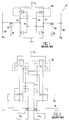
- FIG. 1 there is shown a memory cell 10 implemented in CMOS technology. While this memory cell configuration represents an exemplary cell of a type over which the present invention provides an improvement, it is to be understood that Figures 1, 2 and 6, captioned "RELATED ART", are specifically not admitted to be prior art as to the present invention.
- both P-type and N-type transistors are provided in each of a pair of cross-coupled amplifiers or inverters.
- the P-type MOS transistors are located in a so-called N-well 20 since the formation of different types (N and P) of MOS transistors on a single chip requires different conductivity types of substrate. Accordingly, different conductivity types of substrate are effectively provided by forming a well within a substrate having an impurity type opposite to that of the substrate. While the invention will be described in terms of an N-well in a P-type substrate, as is most common, the conductivity types could be reversed without change in the principles underlying the present invention.
- the memory cell operates as cross coupled push-pull amplifiers; cross-coupling being provided between output nodes 12, 14 and input nodes 16, 18, respectively. Additionally to the bistable latch comprising the memory cell, word line access transistors and bit lines over which the cells are selectively addressed.
- the memory circuitry and the cell within it may also include further peripheral structure to provide a stand-by mode of operation at reduced voltage and power consumption at times other than when a read or write operation is being carried out.
- nodes 12 and 14 In operation, only one of nodes 12 and 14 will be a so-called critical node at any given time.
- the critical node is the node with the high logic level voltage which includes the source and drain regions of transistors N1 and N2 forming the N-type transistor portion of the latch and the word line access transistors NA and NB. Free electrons and holes generated by ionizing radiation (such as an energetic alpha particle) which pass across the diffusion/substrate boundary are collected at the node. The charge collection reduces node voltage and will cause a soft error if the critical charge, Qc, is exceeded.
- FIG. 1 The vulnerability of memory cells such as that of Figure 1 may be more readily appreciated from the exemplary and somewhat idealized layout of the memory cell shown in Figure 2.
- FIG. 6 A variant form reversing the locations of the N-type and P-type transistors is shown in Figure 6 to facilitate comparison with the invention layout illustrated in Figure 5.
- the same reference characters and numerals will be used in all of Figures 1, 2 and 6, insofar as possible.
- the P-type latch transistors, P1 and P2 are, for example, formed in an N-well 20 which is, in turn formed in a P-type substrate.
- N-type latch transistors, N1 and N2 are formed adjacent thereto.
- N-type word line access transistors are preferably formed adjacent to transistors N1 and N2 so that the gates thereof may be formed by word line WL having a relatively linear configuration. It will also be noted from Figures 2 and 6 that the area of the N-type latch transistors is approximately twice the area of the P-type latch transistors for reasons of performance and cell stability (e.g. to prevent change of cell state when the cell is read into the significant capacitance presented by the bit line). Therefore, the N-type latch transistors and the word line access transistors form a relatively large "target" for energetic particles.
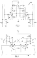
- the invention realizes immunity from soft errors by splitting the critical node (12 or 14 in Figure 2) into two parts (12', 12'' or 14', 14'') and locating the two parts on opposite sides of the N-well in which the P-type latch transistors are formed. This is done by forming separate, parallel connected, N-type latch transistors, N1', N1'' and N2', N2'', (which can then be of reduced size in comparison with transistors N1 and N2 of the memory cell of Figure 2) for each of the cross-coupled amplifiers in the latch.
- the N-well prevents electrons or holes generated by an energetic particle striking on one side of the N-well from affecting the depletion region on the other side of the N-well.
- each of transistors N1'' and N2'' is depicted as formed in the substrate 40 while the remainder of the schematic diagram of Figure 3 remains in schematic form.
- depletion regions 42 will exist in the substrate surrounding doped region 48 corresponding to node 12''.
- a similar depletion region 44 will surround doped region 46 corresponding to node 12' (and transistor N1').
- Depletion regions will also exist around doped regions 56 and 58 (shown in phantom) corresponding to nodes 14' and 14'' (transistors N2' and N2'', respectively).
- doped regions 56 and 58 shown in phantom
- depletion region 42 which is, in essence, a parasitic capacitor
- discharge of the stored charge and reduction of the size of the depletion region 42 to that depicted at 42' may result.
- the charge stored at depletion region 44 will not be affected by the electrons and holes so generated since N-well 20, held at Vcc, is interposed to prevent electrons from reaching the depletion region 44 although voltage will be reduced because the electrode 46 is tied to electrode 48 by a low resistance path connecting nodes 12' and 12''.
- the amount of charge collected will be reduced due to the smaller size of the diffusion at each of nodes 12' and 12''.
- the depletion region 42 has approximately one-half the area of the single depletion region associated with a cell design such as that of Figures 2 and 6, the charge collection is significantly reduced.
- the soft error rate is proportional to the probability the quantity of charge collected exceeds the critical charge required to reverse the cell state.
- the charge collection efficiency is substantially reduced for all conditions except where the energetic particle is so aligned as to strike both depletion regions 42 and 44, which has a statistically negligible probability of occurrence.
- FIG. 5 shows a somewhat idealized, exemplary layout of the memory cell in accordance with the invention.
- the areas of transistors N1', N1'', N2', and N2'' are each reduced by half in comparison with transistors N1 and N2 of Figure 2. Therefore, each of the transistors has only half the likelihood of being affected by an energetic particle as in the memory cell of Figure 2. Additionally, no additional space is occupied by the transistors, as compared with Figures 2 or 6 and the only required increase in size of the memory cell is the space occupied by the required separation between structures on the substrate.
- a second pair of word line access transistors NA2 and NB2 are provided in addition to word line access transistors NA1 and NB1 and selectively connect the output nodes of each of the cross-coupled amplifiers to bit lines BL2a and BL2b in the same manner as selective connection is made to bit lines BL1a and BL1b.
- This selectively parallel connection provides a second port for the memory cell 100.
- the layout of the memory cell in accordance with the present invention by splitting of the critical node, provides a convenient location for the addition of a second port, including transistors NA2 and NB2, controlled by word line WL2.
- This second port is symmetrically located (adjacent one of the transistors of the cross-coupled amplifiers at a position generally opposite the well, across the transistor) and can be formed in the same layers and simultaneously with the first port, thus requiring very little, if any, additional increase in array cell area and limiting the number of process steps required.
- the size (but not the number of processing steps) of the memory cell is increased and then only by about 25% (e.g. 28 square microns to 35.3 square microns) compared with the memory cells of Figures 2 and 6. Even this size penalty can be reduced by formation of additional isolation structures such as isolation trenches at the sides of the N-well to allow reduction of spacing between the NMOS and PMOS transistors.
- isolation between the portions of the critical node could be provided by an isolation trench rather than an N-well.
- the invention provides a memory cell structure with greatly improved immunity to soft errors at virtually no cost in chip space and manufacturing complexity.
- Division and separation of transistors which may form the critical node of the storage cell by a well of opposite conductivity type achieves substantial reduction of charge collection efficiency of diffusion regions when subjected to ionizing radiation such that the probability of collecting a critical amount of charge, Qc is reduced to negligible levels.
- the layout of the memory cell in accordance with the invention also advantageously provides for a second port with no increase in complexity of manufacturing steps or additional layers and with only small increase in required chip space over a single port memory cell.
Landscapes
- Semiconductor Memories (AREA)
- Static Random-Access Memory (AREA)
Abstract
Description
- The present invention generally relates to the structure of cells of static memory devices and, more particularly, to a structure for cells of static memory devices which is substantially immune to so-called soft errors, generally caused by discharging of stored charge due to impact of energetic particles present in the environment.
- Storage of data and instructions in a memory structure is necessary to virtually any data processor application. For this reason, among others, the development of high-performance memory
structures has accompanied the development of data processing circuits and integrated microprocessors in particular. Thus, as integration density and processing power of microprocessors has increased, the same attributes have been sought in memory structures to obtain greater numbers of bits of storage per chip as well as to increase speed of the memory structure. - Memory structures are often considered to fall into one of two groups: dynamic memories and static memories. Dynamic memories offer the greatest potential for reduction of cell size and hence the potential for the greatest amount of storage per chip. Power consumption is also relatively low. On the other hand, the storage mechanism is almost entirely capacitive and, since some degree of leakage is unavoidable in any storage structure, the stored charge representing the stored data must be refreshed periodically. This requirement for periodic refreshing of stored data causes some periods during which the dynamic memory is not available to be read and thus increases the average cycle time and effectively reduces the speed of the response of the memory. Further, the mechanism for reading a dynamic memory essentially requires the use of the stored charge to cause a charge imbalance in a sense amplifier which establishes an appropriate logic voltage output for the memory. However, this operation also requires that the stored charge be rewritten to the cell, further increasing minimum read access time.
- Highest memory read access speed is achieved by static random access memories (SRAMs). In such static memories, the data is stored in a bistable latch comprised of active circuits. Therefore no time is required for either refresh or other operations to restore charge after reading.
- While SRAMs are not generally regarded as relying on stored charge (since, in normal operation, any charge lost through reading or leakage is continually replaced by operation of the active bistable circuit therein), when implemented with field effect transistors, voltages present on various nodes may cause storage of charge in a depletion region within or around a portion of the field effect transistors.
- If an energetic particle from the environment, such as an alpha-particle, strikes an electrode surrounded by such a depletion region, electrons and holes will be generated within the underlying body of semiconductor material and will collect along the boundary of the depletion region. If the energetic particle strikes an electrode (e.g. an N-type transistor holding charge in a depletion region, the size of the depletion region and the voltage on the electrode will be reduced by the charge perturbation. Similarly, if an energetic particle strikes an electrode of a P-type transistor at low voltage, the charge perturbation will cause the voltage to be increased. Thus, if the charge perturbation is sufficiently large, the stored logic state may be reversed. This is commonly referred to as a "soft error" since the error is not due to a hardware defect and the cell will operate normally thereafter (although it may contain erroneous data until rewritten). Soft errors are increased by stand-by operation at reduced voltage.
- Accordingly, a performance parameter of an SRAM storage cell is the critical charge, Qc, which is the amount of charge which will cause logic state reversal of the latch by causing a sufficiently large voltage disturbance. Unfortunately, both miniaturization and lowered operating voltages (migration to 3.3V parts) of SRAM cells with higher integration densities and/or lowered operating voltages also reduce the value of Qc for stable operation of the cell. Accordingly, SRAMs have become increasingly vulnerable to soft errors. Accordingly, many attempts have been made to reduce this vulnerability to soft errors in recent years.
- However, many of these efforts to reduce the incidence of soft errors often require additional electronic elements (such as additional transistors or even some refresh arrangement or redundant storage) which occupy additional space on the chip and reduce the potential degree of integration which is practical. Further, such additional elements often require further process steps or even additional layers to be formed in the semiconductor device, increasing cost and complexity and commonly reducing manufacturing yield. Accordingly, no particularly satisfactory solution to the problem of soft error reduction has heretofore been found.
- Another feature of SRAMS which has recently become of interest is the provision of multiple ports for each cell. That is, the association of each cell with two or more independently operated bit lines. Such a feature allows effectively increased speed of access since a corresponding number of cells on an accessed word line could be read simultaneously or at least within the same memory cycle (since accessed addresses are a combination of the word line and bit line addresses). However, in known memory cell structures, the topology of the bit line access transistor in combination with the conductors forming the bit line and the connection to the bistable circuit are complicated since they have required additional insulator, semiconductor and conductor layers to be provided in the devices. Therefore, memories with more than two ports per cell are largely impractical and even the provision of a second port for each cell disproportionately increases cost and reduces manufacturing yield.
- It is therefore an object of the present invention to provide a structure for a memory cell with markedly improved immunity to soft errors and which will exhibit extremely low soft error rates.
- It is another object of the present invention to provide a two port memory cell structure with simplified topology which can be fabricated with little or no increase in manufacturing steps and at high yield.
- It is a further object of the invention to provide a high performance SRAM cell which is highly immune to soft errors and can readily be formed with at least two ports while not requiring significantly greater chip space than conventional SRAM cells which do not exhibit these properties.
- To achieve the above and other objects of the invention, a memory cell is provided including a semiconductor substrate of a first conductivity type, a well of a second conductivity type formed in the substrate, and two cross-coupled inverters, each including a storage node, the storage node comprising respective portions of each of at least two transistors of each of the cross-coupled inverters, a portion of the well of the second conductivity type being located between the respective portions of each of the at least two transistors.
- In accordance with another aspect of the invention, a memory cell is provided including a storage node formed by at least two spatially separated depletion regions, and an isolation structure located between at least two of the spatially separated depletion regions for reducing collection of charge engendered by ionizing radiation in the vicinity of a first of the at least two spatially separated depletion regions and a second of the at least two spatially separated depletion regions.
- In accordance with a further aspect of the invention, a memory cell is provided including a pair of cross-coupled transistor inverters formed at a surface of a substrate of a first conductivity type, at least two transistors of at least one of said cross-coupled inverters being formed at a surface of said substrate and connected to a storage node of said memory cell, and an isolation structure located in a portion of the surface of the substrate and extending between the at least two transistors.
- The foregoing and other objects, aspects and advantages will be better understood from the following detailed description of a preferred embodiment of the invention with reference to the drawings, in which:
- Figure 1 is an schematic diagram of a memory cell over which the present invention represents an improvement,
- Figure 2 is an diagram of an exemplary layout of the memory cell of Figure 1,
- Figure 3 is an schematic diagram of a memory cell in accordance with the present invention,
- Figure 4 is a hybrid schematic/structural diagram of a portion of a memory cell in accordance with the invention and useful in understanding soft errors and the immunity therefrom provided by the invention,
- Figure 5 is an diagram of an exemplary layout of the memory cell of the invention as shown in Figure 3, and
- Figure 6 is a variant form of the layout of the memory cell of Figure 1 and particularly useful for comparison with the layout of the invention as shown in Figure 5.
- Referring now to the drawings, and more particularly to Figure 1, there is shown a
memory cell 10 implemented in CMOS technology. While this memory cell configuration represents an exemplary cell of a type over which the present invention provides an improvement, it is to be understood that Figures 1, 2 and 6, captioned "RELATED ART", are specifically not admitted to be prior art as to the present invention. - In accordance with CMOS technology, to minimize the number of elements in the
cell 10, both P-type and N-type transistors are provided in each of a pair of cross-coupled amplifiers or inverters. The P-type MOS transistors are located in a so-called N-well 20 since the formation of different types (N and P) of MOS transistors on a single chip requires different conductivity types of substrate. Accordingly, different conductivity types of substrate are effectively provided by forming a well within a substrate having an impurity type opposite to that of the substrate. While the invention will be described in terms of an N-well in a P-type substrate, as is most common, the conductivity types could be reversed without change in the principles underlying the present invention. - As is well-understood in the art, a logic level voltage applied in common to the gate electrodes of P-type and N-type transistors which tends to turn one transistor on will tend to turn the other transistor off. Therefore, the memory cell operates as cross coupled push-pull amplifiers; cross-coupling being provided between
output nodes input nodes - In operation, only one of
nodes - The vulnerability of memory cells such as that of Figure 1 may be more readily appreciated from the exemplary and somewhat idealized layout of the memory cell shown in Figure 2. A variant form reversing the locations of the N-type and P-type transistors is shown in Figure 6 to facilitate comparison with the invention layout illustrated in Figure 5. The same reference characters and numerals will be used in all of Figures 1, 2 and 6, insofar as possible. In Figures 2 and 6, the P-type latch transistors, P1 and P2, are, for example, formed in an N-well 20 which is, in turn formed in a P-type substrate. N-type latch transistors, N1 and N2, are formed adjacent thereto. N-type word line access transistors, NA and NB, are preferably formed adjacent to transistors N1 and N2 so that the gates thereof may be formed by word line WL having a relatively linear configuration. It will also be noted from Figures 2 and 6 that the area of the N-type latch transistors is approximately twice the area of the P-type latch transistors for reasons of performance and cell stability (e.g. to prevent change of cell state when the cell is read into the significant capacitance presented by the bit line). Therefore, the N-type latch transistors and the word line access transistors form a relatively large "target" for energetic particles.
- Referring now to Figures 3 and 4, the circuit and operation of the
memory cell 100 in accordance with the invention will now be explained. In essence, the invention realizes immunity from soft errors by splitting the critical node (12 or 14 in Figure 2) into two parts (12', 12'' or 14', 14'') and locating the two parts on opposite sides of the N-well in which the P-type latch transistors are formed. This is done by forming separate, parallel connected, N-type latch transistors, N1', N1'' and N2', N2'', (which can then be of reduced size in comparison with transistors N1 and N2 of the memory cell of Figure 2) for each of the cross-coupled amplifiers in the latch. Since these transistors have been separated they can be located on opposite sides of the N-well which is preferably connected to Vcc to provide supply voltage to a conduction terminal of each of transistors P1 and P2. Thus, the N-well prevents electrons or holes generated by an energetic particle striking on one side of the N-well from affecting the depletion region on the other side of the N-well. - More specifically, as shown in Figure 4, in which a portion of each of transistors N1'' and N2'' is depicted as formed in the
substrate 40 while the remainder of the schematic diagram of Figure 3 remains in schematic form. Assuming nodes 12' , 12'' to be the critical nodes,depletion regions 42 will exist in the substrate surrounding doped region 48 corresponding to node 12''. Asimilar depletion region 44 will surround dopedregion 46 corresponding to node 12' (and transistor N1'). Depletion regions will also exist around dopedregions 56 and 58 (shown in phantom) corresponding to nodes 14' and 14'' (transistors N2' and N2'', respectively). However, these are not critical nodes and any charge collected will reinforce the cell storage state. - Now, if it is assumed that an incident energetic particle causes generation of electrons and holes in the vicinity of depletion region 42 (which is, in essence, a parasitic capacitor), discharge of the stored charge and reduction of the size of the
depletion region 42 to that depicted at 42' may result. The charge stored atdepletion region 44 will not be affected by the electrons and holes so generated since N-well 20, held at Vcc, is interposed to prevent electrons from reaching thedepletion region 44 although voltage will be reduced because theelectrode 46 is tied to electrode 48 by a low resistance path connecting nodes 12' and 12''. However, the amount of charge collected will be reduced due to the smaller size of the diffusion at each of nodes 12' and 12''. Because thedepletion region 42 has approximately one-half the area of the single depletion region associated with a cell design such as that of Figures 2 and 6, the charge collection is significantly reduced. The soft error rate is proportional to the probability the quantity of charge collected exceeds the critical charge required to reverse the cell state. Thus, even a small reduction in charge collection efficiency can result in a significant reduction in soft error rate as the level of charge collection is reduced below the critical charge. In the case of the present invention, the charge collection efficiency is substantially reduced for all conditions except where the energetic particle is so aligned as to strike bothdepletion regions - Several other advantages of the invention will be readily understood from Figure 5, which shows a somewhat idealized, exemplary layout of the memory cell in accordance with the invention. First, the areas of transistors N1', N1'', N2', and N2'' are each reduced by half in comparison with transistors N1 and N2 of Figure 2. Therefore, each of the transistors has only half the likelihood of being affected by an energetic particle as in the memory cell of Figure 2. Additionally, no additional space is occupied by the transistors, as compared with Figures 2 or 6 and the only required increase in size of the memory cell is the space occupied by the required separation between structures on the substrate.
- Returning briefly to Figure 3, a second pair of word line access transistors NA2 and NB2 are provided in addition to word line access transistors NA1 and NB1 and selectively connect the output nodes of each of the cross-coupled amplifiers to bit lines BL2a and BL2b in the same manner as selective connection is made to bit lines BL1a and BL1b. This selectively parallel connection provides a second port for the
memory cell 100. As shown in Phantom in Figure 5, the layout of the memory cell in accordance with the present invention, by splitting of the critical node, provides a convenient location for the addition of a second port, including transistors NA2 and NB2, controlled by word line WL2. This second port is symmetrically located (adjacent one of the transistors of the cross-coupled amplifiers at a position generally opposite the well, across the transistor) and can be formed in the same layers and simultaneously with the first port, thus requiring very little, if any, additional increase in array cell area and limiting the number of process steps required. In practice, only the size (but not the number of processing steps) of the memory cell is increased and then only by about 25% (e.g. 28 square microns to 35.3 square microns) compared with the memory cells of Figures 2 and 6. Even this size penalty can be reduced by formation of additional isolation structures such as isolation trenches at the sides of the N-well to allow reduction of spacing between the NMOS and PMOS transistors. In the alternative and assuming the PMOS transistors could be located elsewhere, isolation between the portions of the critical node could be provided by an isolation trench rather than an N-well. - In view of the foregoing, it is seen that the invention provides a memory cell structure with greatly improved immunity to soft errors at virtually no cost in chip space and manufacturing complexity. Division and separation of transistors which may form the critical node of the storage cell by a well of opposite conductivity type achieves substantial reduction of charge collection efficiency of diffusion regions when subjected to ionizing radiation such that the probability of collecting a critical amount of charge, Qc is reduced to negligible levels. The layout of the memory cell in accordance with the invention also advantageously provides for a second port with no increase in complexity of manufacturing steps or additional layers and with only small increase in required chip space over a single port memory cell.
Claims (13)
- A memory cell including
a semiconductor substrate of a first conductivity type,
a well of a second conductivity type formed in said substrate, and
two cross-coupled inverters, each of said cross-coupled inverters including a storage node, said storage node comprising respective portions of each of at least two transistors of each of said cross-coupled inverters,
a portion of said well of said second conductivity type being located between said respective portions of each of said at least two transistors. - A memory cell as recited in claim 1, wherein said transistors are field effect transistors.
- A memory cell as recited in claim 1 wherein said transistors are complementary field effect transistors.
- A memory cell as recited in claim 1 or 3, wherein at least one of said cross-coupled inverters further includes a transistor located at said well of said second conductivity type.
- A memory cell as recited in claim 1 or 4, further including a bit line and a word line access transistor connected between said storage node and said bit line.
- A memory cell as recited in claim 1 or 4, further including at least two bit lines and at least two word line access transistors, each said word line access transistor being connected between said storage node and a respective one of said at least two bit lines.
- A memory cell as recited in claim 1, wherein said semiconductor substrate is a P-type semiconductor substrate.
- A memory cell as recited in claim 1, wherein said two cross-coupled amplifiers include complementary metal oxide semiconductor field effect transistors.
- A memory cell including a pair of cross-coupled transistor inverters and formed at a surface of a substrate of a first conductivity type, said memory cell including,
at least two transistors of at least one of said cross-coupled inverters being formed at a surface of said substrate and connected to a storage node of said memory cell,
an isolation structure located in a portion of said surface of said substrate and extending between said at least two transistors. - a memory cell as recited in claim 9, wherein said isolation structure includes a well of a second conductivity type semiconductor material.
- A memory cell as recited in claim 10, further including a further transistor of at least one of said cross-coupled inverters being formed in said well of said second conductivity type.
- A memory cell as recited in claim 9 or 10, further including a first word line access transistor located adjacent one of said at least two transistors and generally opposite to said well of said second conductivity type.
- A memory cell as recited in claim 12, further including a second word line access transistor located adjacent another of said at least two transistors and generally opposite to said well of said second conductivity type.
Applications Claiming Priority (2)
| Application Number | Priority Date | Filing Date | Title |
|---|---|---|---|
| US08/043,090 US5338963A (en) | 1993-04-05 | 1993-04-05 | Soft error immune CMOS static RAM cell |
| US43090 | 1993-04-05 |
Publications (2)
| Publication Number | Publication Date |
|---|---|
| EP0623932A2 true EP0623932A2 (en) | 1994-11-09 |
| EP0623932A3 EP0623932A3 (en) | 1996-03-27 |
Family
ID=21925450
Family Applications (1)
| Application Number | Title | Priority Date | Filing Date |
|---|---|---|---|
| EP94480022A Withdrawn EP0623932A3 (en) | 1993-04-05 | 1994-03-08 | Soft error immune CMOS static RAM cell. |
Country Status (3)
| Country | Link |
|---|---|
| US (1) | US5338963A (en) |
| EP (1) | EP0623932A3 (en) |
| JP (1) | JP2589949B2 (en) |
Cited By (3)
| Publication number | Priority date | Publication date | Assignee | Title |
|---|---|---|---|---|
| WO1998013762A1 (en) * | 1996-09-26 | 1998-04-02 | Philips Electronics N.V. | Processing system and method for reading and restoring information in a ram configuration |
| FR2875328A1 (en) * | 2004-09-15 | 2006-03-17 | St Microelectronics Sa | MEMORY CELL SRAM PROTECTED AGAINST CURRENT OR VOLTAGE PICS |
| CN109669804A (en) * | 2018-11-29 | 2019-04-23 | 中国电子产品可靠性与环境试验研究所((工业和信息化部电子第五研究所)(中国赛宝实验室)) | For reducing the method and apparatus of the practical soft error rate in memory block of ECC memory |
Families Citing this family (44)
| Publication number | Priority date | Publication date | Assignee | Title |
|---|---|---|---|---|
| US5554874A (en) * | 1995-06-05 | 1996-09-10 | Quantum Effect Design, Inc. | Six-transistor cell with wide bit-line pitch, double words lines, and bit-line contact shared among four cells |
| US6330182B1 (en) * | 1998-09-23 | 2001-12-11 | Intel Corporation | Method for evaluating soft error immunity of CMOS circuits |
| JP4885365B2 (en) * | 2000-05-16 | 2012-02-29 | ルネサスエレクトロニクス株式会社 | Semiconductor device |
| JP5420582B2 (en) * | 2000-05-16 | 2014-02-19 | ルネサスエレクトロニクス株式会社 | Semiconductor device |
| JP2001332633A (en) * | 2000-05-24 | 2001-11-30 | Sony Corp | Semiconductor memory |
| US6545330B1 (en) | 2000-07-12 | 2003-04-08 | International Business Machines Corporation | On chip alpha-particle detector |
| JP2002050183A (en) * | 2000-07-31 | 2002-02-15 | Mitsubishi Electric Corp | Semiconductor storage device |
| JP4357101B2 (en) | 2000-08-23 | 2009-11-04 | 株式会社ルネサステクノロジ | Semiconductor memory device |
| US6472715B1 (en) * | 2000-09-28 | 2002-10-29 | Lsi Logic Corporation | Reduced soft error rate (SER) construction for integrated circuit structures |
| TW522546B (en) * | 2000-12-06 | 2003-03-01 | Mitsubishi Electric Corp | Semiconductor memory |
| JP2002353413A (en) | 2001-05-28 | 2002-12-06 | Mitsubishi Electric Corp | Semiconductor storage device |
| JP2003030988A (en) * | 2001-07-12 | 2003-01-31 | Mitsubishi Electric Corp | Semiconductor memory circuit |
| JP2003060087A (en) * | 2001-08-10 | 2003-02-28 | Mitsubishi Electric Corp | Semiconductor storage device |
| US6664141B1 (en) | 2001-08-10 | 2003-12-16 | Lsi Logic Corporation | Method of forming metal fuses in CMOS processes with copper interconnect |
| JP2003152111A (en) | 2001-11-13 | 2003-05-23 | Mitsubishi Electric Corp | Semiconductor storage device |
| JP4073691B2 (en) * | 2002-03-19 | 2008-04-09 | 株式会社ルネサステクノロジ | Semiconductor memory device |
| JP2004047529A (en) * | 2002-07-09 | 2004-02-12 | Renesas Technology Corp | Semiconductor storage device |
| US6826090B1 (en) | 2003-06-05 | 2004-11-30 | International Business Machines Corporation | Apparatus and method for a radiation resistant latch |
| WO2006016403A1 (en) * | 2004-08-10 | 2006-02-16 | Fujitsu Limited | Semiconductor storage device |
| JP4783022B2 (en) * | 2005-01-17 | 2011-09-28 | 株式会社東芝 | Semiconductor integrated circuit device |
| JP5066855B2 (en) * | 2005-07-26 | 2012-11-07 | 富士通株式会社 | SRAM, semiconductor memory device, data maintenance method in SRAM, and electronic device |
| US7446352B2 (en) | 2006-03-09 | 2008-11-04 | Tela Innovations, Inc. | Dynamic array architecture |
| US9230910B2 (en) | 2006-03-09 | 2016-01-05 | Tela Innovations, Inc. | Oversized contacts and vias in layout defined by linearly constrained topology |
| US8448102B2 (en) | 2006-03-09 | 2013-05-21 | Tela Innovations, Inc. | Optimizing layout of irregular structures in regular layout context |
| US8653857B2 (en) | 2006-03-09 | 2014-02-18 | Tela Innovations, Inc. | Circuitry and layouts for XOR and XNOR logic |
| US8839175B2 (en) | 2006-03-09 | 2014-09-16 | Tela Innovations, Inc. | Scalable meta-data objects |
| US8658542B2 (en) | 2006-03-09 | 2014-02-25 | Tela Innovations, Inc. | Coarse grid design methods and structures |
| US8541879B2 (en) | 2007-12-13 | 2013-09-24 | Tela Innovations, Inc. | Super-self-aligned contacts and method for making the same |
| US7956421B2 (en) | 2008-03-13 | 2011-06-07 | Tela Innovations, Inc. | Cross-coupled transistor layouts in restricted gate level layout architecture |
| US9563733B2 (en) | 2009-05-06 | 2017-02-07 | Tela Innovations, Inc. | Cell circuit and layout with linear finfet structures |
| US7763534B2 (en) | 2007-10-26 | 2010-07-27 | Tela Innovations, Inc. | Methods, structures and designs for self-aligning local interconnects used in integrated circuits |
| JP2008085235A (en) * | 2006-09-29 | 2008-04-10 | Toshiba Corp | Semiconductor device |
| US8667443B2 (en) | 2007-03-05 | 2014-03-04 | Tela Innovations, Inc. | Integrated circuit cell library for multiple patterning |
| US7888705B2 (en) | 2007-08-02 | 2011-02-15 | Tela Innovations, Inc. | Methods for defining dynamic array section with manufacturing assurance halo and apparatus implementing the same |
| US20140157223A1 (en) * | 2008-01-17 | 2014-06-05 | Klas Olof Lilja | Circuit and layout design methods and logic cells for soft error hard integrated circuits |
| US8453094B2 (en) | 2008-01-31 | 2013-05-28 | Tela Innovations, Inc. | Enforcement of semiconductor structure regularity for localized transistors and interconnect |
| US7939443B2 (en) | 2008-03-27 | 2011-05-10 | Tela Innovations, Inc. | Methods for multi-wire routing and apparatus implementing same |
| US8072797B2 (en) * | 2008-07-07 | 2011-12-06 | Certichip Inc. | SRAM cell without dedicated access transistors |
| KR101903975B1 (en) | 2008-07-16 | 2018-10-04 | 텔라 이노베이션스, 인코포레이티드 | Methods for cell phasing and placement in dynamic array architecture and implementation of the same |
| US8363455B2 (en) | 2008-12-04 | 2013-01-29 | David Rennie | Eight transistor soft error robust storage cell |
| US8661392B2 (en) | 2009-10-13 | 2014-02-25 | Tela Innovations, Inc. | Methods for cell boundary encroachment and layouts implementing the Same |
| US9159627B2 (en) | 2010-11-12 | 2015-10-13 | Tela Innovations, Inc. | Methods for linewidth modification and apparatus implementing the same |
| JP5705053B2 (en) * | 2011-07-26 | 2015-04-22 | ルネサスエレクトロニクス株式会社 | Semiconductor device |
| US9006827B2 (en) | 2011-11-09 | 2015-04-14 | International Business Machines Corporation | Radiation hardened memory cell and design structures |
Family Cites Families (3)
| Publication number | Priority date | Publication date | Assignee | Title |
|---|---|---|---|---|
| JPS5953637B2 (en) * | 1978-09-20 | 1984-12-26 | 株式会社東芝 | memory circuit |
| JPS6046545B2 (en) * | 1980-05-16 | 1985-10-16 | 日本電気株式会社 | Complementary MOS storage circuit device |
| US5189640A (en) * | 1990-03-27 | 1993-02-23 | National Semiconductor Corporation | High speed, multi-port memory cell utilizable in a BICMOS memory array |
-
1993
- 1993-04-05 US US08/043,090 patent/US5338963A/en not_active Expired - Fee Related
-
1994
- 1994-02-24 JP JP6049989A patent/JP2589949B2/en not_active Expired - Lifetime
- 1994-03-08 EP EP94480022A patent/EP0623932A3/en not_active Withdrawn
Non-Patent Citations (1)
| Title |
|---|
| IBM TECHNICAL DISCLOSURE BULLETIN, vol. 32, no. 8B, January 1990 NEW YORK US, pages 64-65, XP 000082487 'PROCESS FOR SELF-ALIGNED COMMON TWO-GATE, SIX-TRANSISTOR, COMPLEMENTARY METAL OXIDE SILICON STATIC RANDOM-ACCESS MEMORY' * |
Cited By (6)
| Publication number | Priority date | Publication date | Assignee | Title |
|---|---|---|---|---|
| WO1998013762A1 (en) * | 1996-09-26 | 1998-04-02 | Philips Electronics N.V. | Processing system and method for reading and restoring information in a ram configuration |
| FR2875328A1 (en) * | 2004-09-15 | 2006-03-17 | St Microelectronics Sa | MEMORY CELL SRAM PROTECTED AGAINST CURRENT OR VOLTAGE PICS |
| US7535743B2 (en) | 2004-09-15 | 2009-05-19 | Stmicroelectronics S.A. | SRAM memory cell protected against current or voltage spikes |
| US7872894B2 (en) | 2004-09-15 | 2011-01-18 | Stmicroelectronics S.A. | SRAM memory cell protected against current or voltage spikes |
| CN109669804A (en) * | 2018-11-29 | 2019-04-23 | 中国电子产品可靠性与环境试验研究所((工业和信息化部电子第五研究所)(中国赛宝实验室)) | For reducing the method and apparatus of the practical soft error rate in memory block of ECC memory |
| CN109669804B (en) * | 2018-11-29 | 2022-04-19 | 中国电子产品可靠性与环境试验研究所((工业和信息化部电子第五研究所)(中国赛宝实验室)) | Method and apparatus for reducing the actual soft error rate of a storage area of an ECC memory |
Also Published As
| Publication number | Publication date |
|---|---|
| US5338963A (en) | 1994-08-16 |
| JPH077089A (en) | 1995-01-10 |
| EP0623932A3 (en) | 1996-03-27 |
| JP2589949B2 (en) | 1997-03-12 |
Similar Documents
| Publication | Publication Date | Title |
|---|---|---|
| US5338963A (en) | Soft error immune CMOS static RAM cell | |
| USRE47831E1 (en) | Semiconductor memory | |
| US5204990A (en) | Memory cell with capacitance for single event upset protection | |
| US5706226A (en) | Low voltage CMOS SRAM | |
| KR100474602B1 (en) | Semiconductor memory device | |
| US7110318B2 (en) | Semiconductor memory device | |
| US4912675A (en) | Single event upset hardened memory cell | |
| US6744661B1 (en) | Radiation-hardened static memory cell using isolation technology | |
| US6909135B2 (en) | Semiconductor memory device | |
| US5206533A (en) | Transistor device with resistive coupling | |
| JP2518133B2 (en) | Static type semiconductor memory device | |
| US6507511B1 (en) | Secure and dense SRAM cells in EDRAM technology | |
| US5640341A (en) | Memory cell insensitive to collisions of heavy ions | |
| US6888741B2 (en) | Secure and static 4T SRAM cells in EDRAM technology | |
| US20020009002A1 (en) | Semiconductor memory device | |
| JP2756316B2 (en) | Bistable logic device | |
| US7269057B2 (en) | Method for connecting circuit elements within an integrated circuit for reducing single-event upsets | |
| KR102717769B1 (en) | Radiation-hardened memory cell and memory cell array including the same |
Legal Events
| Date | Code | Title | Description |
|---|---|---|---|
| PUAI | Public reference made under article 153(3) epc to a published international application that has entered the european phase |
Free format text: ORIGINAL CODE: 0009012 |
|
| AK | Designated contracting states |
Kind code of ref document: A2 Designated state(s): DE FR GB |
|
| 17P | Request for examination filed |
Effective date: 19950227 |
|
| PUAL | Search report despatched |
Free format text: ORIGINAL CODE: 0009013 |
|
| AK | Designated contracting states |
Kind code of ref document: A3 Designated state(s): DE FR GB |
|
| 17Q | First examination report despatched |
Effective date: 19970718 |
|
| STAA | Information on the status of an ep patent application or granted ep patent |
Free format text: STATUS: THE APPLICATION IS DEEMED TO BE WITHDRAWN |
|
| 18D | Application deemed to be withdrawn |
Effective date: 19980129 |