EP0620460B1 - Semiconductor element module - Google Patents
Semiconductor element module Download PDFInfo
- Publication number
- EP0620460B1 EP0620460B1 EP94105703A EP94105703A EP0620460B1 EP 0620460 B1 EP0620460 B1 EP 0620460B1 EP 94105703 A EP94105703 A EP 94105703A EP 94105703 A EP94105703 A EP 94105703A EP 0620460 B1 EP0620460 B1 EP 0620460B1
- Authority
- EP
- European Patent Office
- Prior art keywords
- sleeve
- hollow portion
- lens
- light
- module according
- Prior art date
- Legal status (The legal status is an assumption and is not a legal conclusion. Google has not performed a legal analysis and makes no representation as to the accuracy of the status listed.)
- Expired - Lifetime
Links
Images


Classifications
-
- G—PHYSICS
- G02—OPTICS
- G02B—OPTICAL ELEMENTS, SYSTEMS OR APPARATUS
- G02B7/00—Mountings, adjusting means, or light-tight connections, for optical elements
- G02B7/02—Mountings, adjusting means, or light-tight connections, for optical elements for lenses
- G02B7/025—Mountings, adjusting means, or light-tight connections, for optical elements for lenses using glue
-
- G—PHYSICS
- G02—OPTICS
- G02B—OPTICAL ELEMENTS, SYSTEMS OR APPARATUS
- G02B6/00—Light guides; Structural details of arrangements comprising light guides and other optical elements, e.g. couplings
- G02B6/24—Coupling light guides
- G02B6/42—Coupling light guides with opto-electronic elements
- G02B6/4201—Packages, e.g. shape, construction, internal or external details
- G02B6/4204—Packages, e.g. shape, construction, internal or external details the coupling comprising intermediate optical elements, e.g. lenses, holograms
-
- H—ELECTRICITY
- H01—ELECTRIC ELEMENTS
- H01L—SEMICONDUCTOR DEVICES NOT COVERED BY CLASS H10
- H01L2224/00—Indexing scheme for arrangements for connecting or disconnecting semiconductor or solid-state bodies and methods related thereto as covered by H01L24/00
- H01L2224/01—Means for bonding being attached to, or being formed on, the surface to be connected, e.g. chip-to-package, die-attach, "first-level" interconnects; Manufacturing methods related thereto
- H01L2224/42—Wire connectors; Manufacturing methods related thereto
- H01L2224/47—Structure, shape, material or disposition of the wire connectors after the connecting process
- H01L2224/48—Structure, shape, material or disposition of the wire connectors after the connecting process of an individual wire connector
- H01L2224/4805—Shape
- H01L2224/4809—Loop shape
- H01L2224/48091—Arched
-
- H—ELECTRICITY
- H01—ELECTRIC ELEMENTS
- H01S—DEVICES USING THE PROCESS OF LIGHT AMPLIFICATION BY STIMULATED EMISSION OF RADIATION [LASER] TO AMPLIFY OR GENERATE LIGHT; DEVICES USING STIMULATED EMISSION OF ELECTROMAGNETIC RADIATION IN WAVE RANGES OTHER THAN OPTICAL
- H01S5/00—Semiconductor lasers
- H01S5/02—Structural details or components not essential to laser action
- H01S5/022—Mountings; Housings
- H01S5/02208—Mountings; Housings characterised by the shape of the housings
- H01S5/02212—Can-type, e.g. TO-CAN housings with emission along or parallel to symmetry axis
-
- H—ELECTRICITY
- H01—ELECTRIC ELEMENTS
- H01S—DEVICES USING THE PROCESS OF LIGHT AMPLIFICATION BY STIMULATED EMISSION OF RADIATION [LASER] TO AMPLIFY OR GENERATE LIGHT; DEVICES USING STIMULATED EMISSION OF ELECTROMAGNETIC RADIATION IN WAVE RANGES OTHER THAN OPTICAL
- H01S5/00—Semiconductor lasers
- H01S5/02—Structural details or components not essential to laser action
- H01S5/022—Mountings; Housings
- H01S5/0225—Out-coupling of light
- H01S5/02251—Out-coupling of light using optical fibres
Definitions
- the present invention relates to a semiconductor element module used in a reception unit and a transmission unit in an optical communication system.
- An optical communication system using an optical fiber technique has been attracting attention in recent years. Since light-emitting and light-receiving elements are generally very small and are inconvenient for use as they are, they are usually provided in a semiconductor element module. A sleeve is formed in this semiconductor element module to connect this module to a ferrule having an optical fiber inserted therein.
- a light-emitting diode is generally used as a light-emitting element. Since emitted light diffuses, the light is generally converged by a lens and guided into the optical fiber. Since light emitting from the end face of the optical fiber also diffuses, a lens must be provided between the optical fiber and the light-receiving element, thereby improving the ratio of light guided to the light-receiving element.
- a lens must be provided between a semiconductor element, e.g., a light-emitting or light-receiving element, and the optical fiber.
- An example of conventional modules has a structure in which a lens is directly provided to a semiconductor element (e.g., Japanese Patent Laid-Open No. 4-165312 and the like).
- the other example has a structure in which a lens is provided in a module.
- SUS430 which is a material having a thermal expansion coefficient close to that of a glass material constituting the lens is used as the material of the metal cylinder holding the lens.
- SUS303-based material having a good machining performance is used as the material constituting the sleeve.
- a light-emitting element is hermetically sealed by using a cap 201 that fixes a lens 220, and the cap 201 is mounted to a sleeve.
- the sleeve is made of a corrosion-resistant metal, namely ferrite-based stainless steel, such as an SUS430 or an SUS430F metal.
- the converging lens is preferably made of BK7 optical glass. And TaF-3, HE-2, K-2, LF-5, F-3, SF-2, and LaF-3 optical glass are also usable.
- the converging lens is preferably hermetically fixed to close the third hollow portion, and the stem is preferably hermetically fixed to close the other open end.
- the converging lens is preferably fixed to the lens holding portion with a low-melting glass or an inorganic or organic glue.
- the third hollow portion holding the lens and the first hollow portion in which the ferrule is to be inserted are integrally formed as a sleeve, they are coaxial with each other at a high preciseness. Therefore, the centering operation about the optical fiber, the lens, and the semiconductor element which is required when the optical fiber is fitted in the sleeve through the ferrule and the stem fixing the semiconductor element (a light-emitting or light-receiving element) is mounted to the sleeve can be performed easily. Since the first and second hollow portions are integrally formed as the sleeve by using the same material, the number of components can be decreased.
- the thermal expansion coefficient of the material constituting the sleeve and that of the material constituting the lens are close to each other, even if the module is exposed to a large temperature change, a gap will not be formed between the sleeve and the lens, and the material glueing the lens and the sleeve will not be separated.
- ferrite-based stainless steel such as the SUS430 or the SUS430F is used as the material of the sleeve, cohesion of the sleeve and the ferrule can be avoided.
- the third hollow portion holding the lens and the first hollow portion are integrally formed as the sleeve by using the same material, the centering operation about the optical fiber, the lens, and the semiconductor element which is required when the optical fiber is fitted in the first hollow portion and the stem fixing the semiconductor element (light-emitting or light-receiving element) is mounted to the sleeve can be easily performed, and the optical axes of these components can be aligned at a high precision. Also, the number of components can be decreased. Therefore, the manufacturing cost can be decreased, and the yield can be increased.
- the thermal expansion coefficient of the material constituting the sleeve and that of the material constituting the lens are close to each other, even if a large temperature change occurs, a gap will not be formed between the sleeve and the lens, and the material adhering the lens and the sleeve will not be separated. Therefore, the air-tightness of the second hollow portion can be maintained even if a large temperature change takes place.
- ferrite-based stainless steel such as the SUS430 or the SUS430F is used as the material of the sleeve, cohesion of the sleeve and the ferrule can be avoided.
- a high-reliability, low-cost, high-performance semiconductor element module can be provided.
- a fitting portion 11 serving as the first hollow portion in which an optical fiber positioning ferrule is to be fitted is formed in a sleeve 1 from one open end toward its interior.
- An element housing portion 13 serving as the second hollow portion coaxial with the fitting portion 11 is formed in the sleeve 1 from the other open end toward its interior.
- the inner diameter of the element housing portion 13 is larger than that of the fitting portion 11.
- a lens holding portion 12 serving as the third hollow portion is defined in the sleeve 1 by linking the first and second hollow portions.
- the inner diameter of the lens holding portion 12 is smaller than that of the fitting portion 11.
- the sleeve 1 is made of SUS430F metal.
- the inner circumferential surface of the distal end portion of the fitting portion 11 is formed in a tapered manner to be wider toward the outer portion. This aims at facilitating fitting of the ferrule.
- the distal end portion is tapered so that it functions as a ferrule guide.
- the wall of the lens holding portion 12 is thicker than that of the fitting portion 11, and a ball lens 20 is fixed in the inner side of the lens holding portion 12 with a low-melting glass.
- the low-melting glass is a glass to which selenium, thallium, arsenic, or sulfur is added to give low melting points.
- the lens material of the ball lens 20 is BK7 optical glass.
- the material for fixing the ball lens 20, an organic glue, an inorganic glue, or the like can be used in place of the low-melting glass.
- a disk-shaped stem 31 is fixed to the open end of the sleeve 1 on the element housing portion 13 side by projection welding.
- the element housing portion 13 is hermetically maintained, and its interior is a dry N 2 gas atmosphere.
- dust or a corrosive gas will not enter the element housing portion 13 from the outside, thereby obtaining a high reliability.
- the interior of the element housing portion 13 is not limited to the N 2 gas atmosphere but can be other inert gas atmospheres, e.g., an Ar gas atmosphere, or can be set at a vacuum state.
- the stem 31 is obtained by plating Ni to cold-rolled steel and plating Au to the Ni-plated cold-rolled steel.
- a semiconductor light-emitting element 41 is placed on the upper surface of the stem 31.
- Three stem pins 32a, 32b, and 32c are attached to predetermined positions, as shown in Fig. 3, of the stem 31 respectively through seal tubes 34.
- the upper ends of the stem pins 32a, 32b, and 32c projecting through the upper surface of the stem 31 are connected to the semiconductor light-emitting element 41 respectively through wires 33.
- the stem pin 32b may be directly welded to the stem 31 to serve as a ground terminal, thereby providing an electromagnetic shield effect.
- the fitting portion 11 and the lens holding portion 12 of the sleeve 1 are integrally formed using the same material, one centering operation is sufficient for aligning the light-emitting element and the optical fiber. More specifically, the ball lens 20 can be positioned only by fixing it in the lens holding portion 12 of the sleeve 1, and centering can be performed only by fitting the ferrule having an optical fiber in the fitting portion 11 and aligning the stem 31, to which the semiconductor light-emitting element 41 is fixed, to the open end of the sleeve 1. Thus, the centering operation becomes easy to increase the yield, and the machining cost can be decreased. Also, since the entire structure is made of the same material, the number of components can be decreased.
- the sleeve 1 may be formed in accordance with, e.g., coaxial machining by using an NC lathe.
- coaxial machining is performed by using the NC lathe, the coaxial degree of the fitting portion 11 and the lens holding portion 12 can be increased.
- the optical axis of the optical fiber and the center of the ball lens 20 can be aligned at a high precision only by fitting and fixing the ball lens 20 in the lens holding portion 12.
- the SUS430F metal is used as the material of the sleeve 1.
- a corrosion-resistant metal namely ferrite-based stainless steel such as an SUS430 may also be used.
- ferrite-based stainless steel such as an SUS430 or an SUS430F is used, cohesion of the ferrule and the sleeve can be prevented even if the connecting/disconnecting operation of the ferrule is repeated.
- the material of the ball lens 20 As the material of the ball lens 20, BK7 optical glass is used. However, any other material can be used as far as it has a thermal expansion coefficient close to that of the metal constituting the sleeve.
- the material of the ball lens may be determined first and a metal having a thermal expansion coefficient close to that of the material of the ball lens may be selected to form the sleeve, or the metal of the sleeve may be determined first and a material having a thermal expansion coefficient close to that of the metal of the sleeve may be selected to form the ball lens.
- the module can be used as the light-receiving element module.
- the ball lens converges the exit light from the optical fiber onto the light-receiving end face of the light-receiving element.
Description
- The present invention relates to a semiconductor element module used in a reception unit and a transmission unit in an optical communication system.
- An optical communication system using an optical fiber technique has been attracting attention in recent years. Since light-emitting and light-receiving elements are generally very small and are inconvenient for use as they are, they are usually provided in a semiconductor element module. A sleeve is formed in this semiconductor element module to connect this module to a ferrule having an optical fiber inserted therein.
- A light-emitting diode is generally used as a light-emitting element. Since emitted light diffuses, the light is generally converged by a lens and guided into the optical fiber. Since light emitting from the end face of the optical fiber also diffuses, a lens must be provided between the optical fiber and the light-receiving element, thereby improving the ratio of light guided to the light-receiving element.
- Hence, a lens must be provided between a semiconductor element, e.g., a light-emitting or light-receiving element, and the optical fiber. An example of conventional modules has a structure in which a lens is directly provided to a semiconductor element (e.g., Japanese Patent Laid-Open No. 4-165312 and the like). And the other example has a structure in which a lens is provided in a module. When a lens is provided in a module, a
metal holder 101 holding alens 120 therein, as shown in Fig. 1, is mounted to a sleeve (not shown) which is formed separately from themetal holder 101. To hold a lens in a metal holder, a lens is held on a metal cylinder or the like. - At this time, SUS430 which is a material having a thermal expansion coefficient close to that of a glass material constituting the lens is used as the material of the metal cylinder holding the lens. And an SUS303-based material having a good machining performance is used as the material constituting the sleeve.
- Alternatively, as shown in Fig. 2, a light-emitting element is hermetically sealed by using a
cap 201 that fixes alens 220, and thecap 201 is mounted to a sleeve. - In DE-A-40 22 076 a semiconductor element having an optical semiconductor and an optical fiber receptacle into which an optical fiber ferrule may be inserted is described, but without solving the problems of adhesion between the optical element receptacle and the optical fiber ferrule.
- It is an object of the present invention to provide a semiconductor element module for optical communication which has a small number of components and a high endurance against a connecting/disconnecting operation and which can be aligned easily.
- According to the present invention, there is provided a semiconductor element module according to claim 1.
- In the above semiconductor element module, the sleeve is made of a corrosion-resistant metal, namely ferrite-based stainless steel, such as an SUS430 or an SUS430F metal.
- The converging lens is preferably made of BK7 optical glass. And TaF-3, HE-2, K-2, LF-5, F-3, SF-2, and LaF-3 optical glass are also usable.
- The converging lens is preferably hermetically fixed to close the third hollow portion, and the stem is preferably hermetically fixed to close the other open end. The converging lens is preferably fixed to the lens holding portion with a low-melting glass or an inorganic or organic glue.
- According to the above arrangement, since the third hollow portion holding the lens and the first hollow portion in which the ferrule is to be inserted are integrally formed as a sleeve, they are coaxial with each other at a high preciseness. Therefore, the centering operation about the optical fiber, the lens, and the semiconductor element which is required when the optical fiber is fitted in the sleeve through the ferrule and the stem fixing the semiconductor element (a light-emitting or light-receiving element) is mounted to the sleeve can be performed easily. Since the first and second hollow portions are integrally formed as the sleeve by using the same material, the number of components can be decreased.
- Furthermore, since the thermal expansion coefficient of the material constituting the sleeve and that of the material constituting the lens are close to each other, even if the module is exposed to a large temperature change, a gap will not be formed between the sleeve and the lens, and the material glueing the lens and the sleeve will not be separated.
- When the lens and the stem are fixed to the sleeve in tight contact therewith, the air-tightness of the second hollow portion housing the semiconductor element is maintained. Hence, impurities will not enter the second hollow portion from the outside.
- If ferrite-based stainless steel, such as the SUS430 or the SUS430F is used as the material of the sleeve, cohesion of the sleeve and the ferrule can be avoided.
- As described above, according to the present invention, since the third hollow portion holding the lens and the first hollow portion are integrally formed as the sleeve by using the same material, the centering operation about the optical fiber, the lens, and the semiconductor element which is required when the optical fiber is fitted in the first hollow portion and the stem fixing the semiconductor element (light-emitting or light-receiving element) is mounted to the sleeve can be easily performed, and the optical axes of these components can be aligned at a high precision. Also, the number of components can be decreased. Therefore, the manufacturing cost can be decreased, and the yield can be increased.
- Since the thermal expansion coefficient of the material constituting the sleeve and that of the material constituting the lens are close to each other, even if a large temperature change occurs, a gap will not be formed between the sleeve and the lens, and the material adhering the lens and the sleeve will not be separated. Therefore, the air-tightness of the second hollow portion can be maintained even if a large temperature change takes place.
- Since the lens and stem are fixed to the sleeve in tight contact therewith, the air-tightness of the second hollow portion is maintained. Hence, impurities will not enter the second hollow portion from the outside. Therefore, a semiconductor element module having a high reliability can be obtained.
- If ferrite-based stainless steel, such as the SUS430 or the SUS430F is used as the material of the sleeve, cohesion of the sleeve and the ferrule can be avoided.
- Thus, according to the present invention, a high-reliability, low-cost, high-performance semiconductor element module can be provided.
- The present invention will become more fully understood from the detailed description given hereinbelow and the accompanying drawings which are given by way of illustration only, and thus are not to be considered as limiting the present invention.
- Further scope of applicability of the present invention will become apparent from the detailed description given hereinafter. However, it should be understood that the detailed description and specific examples, while indicating preferred embodiments of the invention, are given by way of illustration only.
-
- Fig. 1 is a diagram of a conventional semiconductor element module;
- Fig. 2 is a diagram of another conventional semiconductor element module;
- Fig. 3 is a cut-away perspective view of a semiconductor element module according to an embodiment of the present invention; and
- Fig. 4 is a diagram of the semiconductor element module according to the embodiment of the present invention.
-
- The embodiment of the present invention will be described with reference to the accompanying drawings.
- In the description of the drawings, the same elements will be denoted by the same reference numerals.
- The embodiment of the present invention will be described with reference to Figs. 3 and 4.
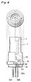
- As shown in Figs. 3 and 4, a fitting
portion 11 serving as the first hollow portion in which an optical fiber positioning ferrule is to be fitted is formed in a sleeve 1 from one open end toward its interior. Anelement housing portion 13 serving as the second hollow portion coaxial with thefitting portion 11 is formed in the sleeve 1 from the other open end toward its interior. The inner diameter of theelement housing portion 13 is larger than that of thefitting portion 11. Alens holding portion 12 serving as the third hollow portion is defined in the sleeve 1 by linking the first and second hollow portions. The inner diameter of thelens holding portion 12 is smaller than that of thefitting portion 11. The sleeve 1 is made of SUS430F metal. - The inner circumferential surface of the distal end portion of the
fitting portion 11 is formed in a tapered manner to be wider toward the outer portion. This aims at facilitating fitting of the ferrule. In other words, the distal end portion is tapered so that it functions as a ferrule guide. - The wall of the
lens holding portion 12 is thicker than that of thefitting portion 11, and aball lens 20 is fixed in the inner side of thelens holding portion 12 with a low-melting glass. The low-melting glass is a glass to which selenium, thallium, arsenic, or sulfur is added to give low melting points. The lens material of theball lens 20 is BK7 optical glass. The material for fixing theball lens 20, an organic glue, an inorganic glue, or the like can be used in place of the low-melting glass. - A disk-shaped
stem 31 is fixed to the open end of the sleeve 1 on theelement housing portion 13 side by projection welding. - The
element housing portion 13 is hermetically maintained, and its interior is a dry N2 gas atmosphere. When theelement housing portion 13 is hermetically maintained in this manner, dust or a corrosive gas will not enter theelement housing portion 13 from the outside, thereby obtaining a high reliability. - As a method of glueing the
stem 31 to the sleeve 1, a solder sealing method and the like are available in addition to projection welding. The interior of theelement housing portion 13 is not limited to the N2 gas atmosphere but can be other inert gas atmospheres, e.g., an Ar gas atmosphere, or can be set at a vacuum state. - The
stem 31 is obtained by plating Ni to cold-rolled steel and plating Au to the Ni-plated cold-rolled steel. A semiconductor light-emittingelement 41 is placed on the upper surface of thestem 31. Threestem pins stem 31 respectively throughseal tubes 34. The upper ends of the stem pins 32a, 32b, and 32c projecting through the upper surface of thestem 31 are connected to the semiconductor light-emittingelement 41 respectively throughwires 33. Thestem pin 32b may be directly welded to thestem 31 to serve as a ground terminal, thereby providing an electromagnetic shield effect. - As described above, according to the semiconductor element module of this embodiment, since the
fitting portion 11 and thelens holding portion 12 of the sleeve 1 are integrally formed using the same material, one centering operation is sufficient for aligning the light-emitting element and the optical fiber. More specifically, theball lens 20 can be positioned only by fixing it in thelens holding portion 12 of the sleeve 1, and centering can be performed only by fitting the ferrule having an optical fiber in thefitting portion 11 and aligning thestem 31, to which the semiconductor light-emittingelement 41 is fixed, to the open end of the sleeve 1. Thus, the centering operation becomes easy to increase the yield, and the machining cost can be decreased. Also, since the entire structure is made of the same material, the number of components can be decreased. - To form the sleeve 1 as indicated in the above embodiment, it may be formed in accordance with, e.g., coaxial machining by using an NC lathe. When coaxial machining is performed by using the NC lathe, the coaxial degree of the
fitting portion 11 and thelens holding portion 12 can be increased. When the coaxial degree of thefitting portion 11 and thelens holding portion 12 is increased, the optical axis of the optical fiber and the center of theball lens 20 can be aligned at a high precision only by fitting and fixing theball lens 20 in thelens holding portion 12. - In the above embodiment, the SUS430F metal is used as the material of the sleeve 1. However, other than this, a corrosion-resistant metal, namely ferrite-based stainless steel such as an SUS430 may also be used. When ferrite-based stainless steel, such as an SUS430 or an SUS430F is used, cohesion of the ferrule and the sleeve can be prevented even if the connecting/disconnecting operation of the ferrule is repeated.
- As the material of the
ball lens 20, BK7 optical glass is used. However, any other material can be used as far as it has a thermal expansion coefficient close to that of the metal constituting the sleeve. In other words, the material of the ball lens may be determined first and a metal having a thermal expansion coefficient close to that of the material of the ball lens may be selected to form the sleeve, or the metal of the sleeve may be determined first and a material having a thermal expansion coefficient close to that of the metal of the sleeve may be selected to form the ball lens. When the thermal expansion coefficients of the ball lens and the metal forming the sleeve are close in this manner, even if a large temperature change occurs, a gap will not be formed between the ball lens and the lens holding portion, and the organic material or the like which adheres the ball lens and the lens holding portion will not be removed. As a result, the air-tightness in theelement housing portion 13 can be maintained even if a large temperature change occurs. - If a light-receiving element is housed in the
element housing portion 13 shown in the above embodiment, the module can be used as the light-receiving element module. In this case, the ball lens converges the exit light from the optical fiber onto the light-receiving end face of the light-receiving element. - From the invention thus described, it will be obvious that the invention may be varied in many ways.
Claims (6)
- A semiconductor element module comprising:a sleeve (1) having a first hollow portion (11) defining a first open end thereof, which hollow portion extends toward an interior portion of said sleeve wherein a ferrule for positioning an optical fiber is adopted to fit in said first hollow portion (11), a second hollow portion (13) defined in a second end of said sleeve, said second hollow portion being coaxial with the first hollow portion (11) and formed having a second open end which is opposite to said first open end, said second hollow portion extending toward the interior portion of said sleeve, and a third hollow portion (12) formed to link the first and second hollow portions (11, 13),a converging lens (20), housed in the third hollow portion (12) and hermetically fixed to said sleeve (1) in order to seal said third hollow portion, for optically coupling an end face of said optical fiber to a light-emitting or light-receiving end face of said optical active element (41),
characterized by said sleeve consisting of a metal selected from the group consisting of ferrite-based stainless steel, such as SUS430 or SUS430F;a stem (31) hermetically fixed to said sleeve (1) and sealing the second open end thereof;an optical active element (41) fixed on a surface of said stem (31); and
wherein said metal (1) has a thermal expansion coefficient which has a correlation expressed by the following equation with a thermal expansion coefficient of a material constituting said converging lens (20):and said sleeve is integrally formed using said metal.κ1 : a thermal expansion coefficient of the sleeveκ2 : a thermal expansion coefficient of the lens. - A module according to claim 1, wherein said sleeve consists of a corrosion-resistant metal.
- A module according to claim 1 or 2, wherein said converging lens (20) consists of a material selected from the group consisting of BK7, TaF-3, HE-2, K-3, LF-5, F-3, SF-2, and LaF-3 optical glass.
- A module according to any of claims 1 to 5, wherein said converging lens (20) is fixed to the third hollow portion (12) with a material selected from the group consisting of a low-melting point glass, an inorganic glue, and an organic glue.
- A module according to any of claims 1 to 4, wherein said optical active element (41) is a semiconductor light-emitting element.
- A module according to any of claims 1 to 4, wherein said optical active element (41) is a semiconductor light-receiving element.
Applications Claiming Priority (3)
| Application Number | Priority Date | Filing Date | Title |
|---|---|---|---|
| JP9005993 | 1993-04-16 | ||
| JP5090059A JPH06300943A (en) | 1993-04-16 | 1993-04-16 | Semiconductor element module |
| JP90059/93 | 1993-04-16 |
Publications (2)
| Publication Number | Publication Date |
|---|---|
| EP0620460A1 EP0620460A1 (en) | 1994-10-19 |
| EP0620460B1 true EP0620460B1 (en) | 2000-08-16 |
Family
ID=13988007
Family Applications (1)
| Application Number | Title | Priority Date | Filing Date |
|---|---|---|---|
| EP94105703A Expired - Lifetime EP0620460B1 (en) | 1993-04-16 | 1994-04-13 | Semiconductor element module |
Country Status (8)
| Country | Link |
|---|---|
| US (1) | US5452389A (en) |
| EP (1) | EP0620460B1 (en) |
| JP (1) | JPH06300943A (en) |
| KR (1) | KR0179057B1 (en) |
| CA (1) | CA2120964C (en) |
| DE (1) | DE69425521T2 (en) |
| DK (1) | DK0620460T3 (en) |
| ES (1) | ES2150957T3 (en) |
Families Citing this family (29)
| Publication number | Priority date | Publication date | Assignee | Title |
|---|---|---|---|---|
| US5764838A (en) * | 1995-09-05 | 1998-06-09 | Nippon Aspherical Lens Co., Ltd. | Aspherical lens for optical fiber and optically coupling construction using the same |
| KR0171844B1 (en) * | 1995-11-10 | 1999-05-01 | 김광호 | Optical connector using ball lens and producing process thereof |
| US6283644B1 (en) * | 1996-01-18 | 2001-09-04 | Stratos Lightwave, Inc. | Optical package with alignment means and method of assembling an optical package |
| US5815623A (en) * | 1996-01-18 | 1998-09-29 | Methode Electronics, Inc. | Optical package with alignment means and method of assembling an optical package |
| US6550983B1 (en) * | 1996-01-18 | 2003-04-22 | Stratos Lightwave Llc | Optical package with alignment means and method of assembling an optical package |
| US5812717A (en) * | 1996-01-18 | 1998-09-22 | Methode Electronics, Inc. | Optical package with alignment means and method of assembling an optical package |
| US6071017A (en) * | 1996-01-18 | 2000-06-06 | Methode Electronics, Inc. | Optical package with alignment means and method of assembling an optical package |
| JPH09218324A (en) * | 1996-02-08 | 1997-08-19 | Alps Electric Co Ltd | Light emission module |
| JP3310910B2 (en) * | 1997-06-24 | 2002-08-05 | 日本板硝子株式会社 | Optical module |
| US5940564A (en) * | 1997-08-05 | 1999-08-17 | Picolight, Inc. | Device for coupling a light source or receiver to an optical waveguide |
| JPH11231177A (en) * | 1997-12-12 | 1999-08-27 | Oki Electric Ind Co Ltd | Optical element module and manufacture of the optical element module |
| US6243508B1 (en) | 1999-06-01 | 2001-06-05 | Picolight Incorporated | Electro-opto-mechanical assembly for coupling a light source or receiver to an optical waveguide |
| TW449948B (en) * | 1999-06-29 | 2001-08-11 | Rohm Co Ltd | Semiconductor device |
| US6325551B1 (en) | 1999-12-08 | 2001-12-04 | New Focus, Inc. | Method and apparatus for optically aligning optical fibers with optical devices |
| TW474056B (en) * | 1999-12-10 | 2002-01-21 | Sumitomo Electric Industries | Optical semiconductor module |
| US6632029B1 (en) | 1999-12-22 | 2003-10-14 | New Focus, Inc. | Method & apparatus for packaging high frequency components |
| US6540412B2 (en) * | 2000-02-10 | 2003-04-01 | Sumitomo Electric Industries, Ltd. | Optical transceiver |
| US6812057B2 (en) * | 2000-07-07 | 2004-11-02 | Nippon Sheet Glass Co., Ltd. | Method of producing an optical module |
| JP2002043675A (en) * | 2000-07-25 | 2002-02-08 | Nippon Sheet Glass Co Ltd | Optical module |
| JP2003185892A (en) | 2001-12-19 | 2003-07-03 | Sumitomo Electric Ind Ltd | Optical connecting sleeve, optical module and optical communication module |
| WO2003052479A1 (en) * | 2001-12-19 | 2003-06-26 | Sumitomo Electric Industries, Ltd. | Optical connection sleeve, optical module, and optical communication module |
| US20050141820A1 (en) * | 2003-10-01 | 2005-06-30 | Tyco Electronics Corporation | Optoelectric package |
| JP4965201B2 (en) | 2005-12-09 | 2012-07-04 | 株式会社エンプラス | Optical module holder, optical module and optical connector |
| KR100746260B1 (en) * | 2007-01-30 | 2007-08-03 | (주)디나옵틱스 | Ball lans unit for transmitter/receiver optical sub assembly of transceiver, and apparatus and method for manufacturing the same |
| EP2592455A3 (en) * | 2010-03-31 | 2013-11-20 | University Court Of The University Of St Andrews | Integreated illuminator |
| JP5947490B2 (en) * | 2011-04-12 | 2016-07-06 | 三菱鉛筆株式会社 | Optical collimator |
| JP6411088B2 (en) * | 2013-09-26 | 2018-10-24 | オリンパス株式会社 | Optical transmission module and endoscope |
| CN108957619B (en) * | 2018-07-25 | 2022-09-27 | 京东方科技集团股份有限公司 | Light guide assembly, manufacturing method of light guide assembly and backlight source |
| CN114614338B (en) * | 2022-02-24 | 2023-06-27 | 中国电子科技集团公司第二十九研究所 | High-reliability laser output optical fiber packaging structure |
Family Cites Families (12)
| Publication number | Priority date | Publication date | Assignee | Title |
|---|---|---|---|---|
| DE3429282A1 (en) * | 1984-08-08 | 1985-04-11 | Siemens AG, 1000 Berlin und 8000 München | Optoelectronic module |
| US4726648A (en) * | 1985-02-13 | 1988-02-23 | Siemens Aktiengesellschaft | Optoelectronic module |
| JPS6279213U (en) * | 1985-11-01 | 1987-05-21 | ||
| US4752743A (en) * | 1986-09-26 | 1988-06-21 | Varian Associates, Inc. | Linearizer for TWT amplifiers |
| EP0407919B1 (en) * | 1989-07-11 | 1996-04-24 | Harmonic Lightwaves, Inc. | Optical transmitters linearized by means of parametric feedback |
| US5127072A (en) * | 1990-03-08 | 1992-06-30 | Ortel Corporation | Laser module with compliant optical fiber coupling |
| DE4022076A1 (en) * | 1990-07-10 | 1992-01-16 | Siemens Ag | Optical coupler for opto-electronic component - has spherical lens enclosed by sleeve fitted to end of optical fibre |
| JPH04165312A (en) * | 1990-10-30 | 1992-06-11 | Nikko Kyodo Co Ltd | Photo module and manufacture thereof |
| JPH04309907A (en) * | 1991-04-09 | 1992-11-02 | Mitsubishi Electric Corp | Manufacture of photosemiconductor element module |
| US5146526A (en) * | 1991-04-12 | 1992-09-08 | Amoco Corporation | Laser pigtail assembly and method |
| JP2763016B2 (en) * | 1991-12-25 | 1998-06-11 | 日本電気株式会社 | Optical element substrate mounting structure |
| US5291571A (en) * | 1992-03-19 | 1994-03-01 | Fujitsu Limited | Duplicated light source module |
-
1993
- 1993-04-16 JP JP5090059A patent/JPH06300943A/en active Pending
-
1994
- 1994-04-08 US US08/224,714 patent/US5452389A/en not_active Expired - Lifetime
- 1994-04-11 CA CA002120964A patent/CA2120964C/en not_active Expired - Fee Related
- 1994-04-13 DE DE69425521T patent/DE69425521T2/en not_active Expired - Fee Related
- 1994-04-13 DK DK94105703T patent/DK0620460T3/en active
- 1994-04-13 EP EP94105703A patent/EP0620460B1/en not_active Expired - Lifetime
- 1994-04-13 ES ES94105703T patent/ES2150957T3/en not_active Expired - Lifetime
- 1994-04-15 KR KR1019940007906A patent/KR0179057B1/en not_active IP Right Cessation
Also Published As
| Publication number | Publication date |
|---|---|
| DK0620460T3 (en) | 2000-12-18 |
| US5452389A (en) | 1995-09-19 |
| KR0179057B1 (en) | 1999-05-15 |
| CA2120964C (en) | 2004-06-29 |
| JPH06300943A (en) | 1994-10-28 |
| ES2150957T3 (en) | 2000-12-16 |
| DE69425521T2 (en) | 2001-04-26 |
| EP0620460A1 (en) | 1994-10-19 |
| DE69425521D1 (en) | 2000-09-21 |
| CA2120964A1 (en) | 1994-10-17 |
Similar Documents
| Publication | Publication Date | Title |
|---|---|---|
| EP0620460B1 (en) | Semiconductor element module | |
| US4803689A (en) | Semiconductor laser module | |
| EP0304182B1 (en) | Fibre tailed opto-electronic transducer | |
| US4707066A (en) | Glass fiber bushing through a wall opening of a housing and method of manufacture | |
| US4616899A (en) | Methods of and apparatus for coupling an optoelectronic component to an optical fiber | |
| EP0404053B1 (en) | Photo-semiconductor module | |
| US5315609A (en) | Semiconductor laser module with lens holder compensating for thermal stress | |
| US5247530A (en) | Laser diode module | |
| JP2628774B2 (en) | Semiconductor laser module with built-in optical isolator | |
| US7090412B2 (en) | Optical module | |
| JPH02124504A (en) | Photodetecting module | |
| US20040042071A1 (en) | Light emitting modules | |
| JP2945246B2 (en) | Optical element module | |
| JPS59166907A (en) | Semiconductor laser coupling device | |
| JP2586123B2 (en) | Semiconductor laser module | |
| JP2940497B2 (en) | Optical semiconductor module | |
| JPH0569406B2 (en) | ||
| JP4308049B2 (en) | Semiconductor element module | |
| JP3960073B2 (en) | Optical link device | |
| JPH0232307A (en) | Optical semiconductor element module | |
| JPS6074686A (en) | Cap | |
| JPS62261183A (en) | Optical element module | |
| JPH0396905A (en) | Photosemiconductor module | |
| JPH03158804A (en) | Photoelectronic device with optical coupler | |
| JPH1039174A (en) | Semiconductor laser module device |
Legal Events
| Date | Code | Title | Description |
|---|---|---|---|
| PUAI | Public reference made under article 153(3) epc to a published international application that has entered the european phase |
Free format text: ORIGINAL CODE: 0009012 |
|
| AK | Designated contracting states |
Kind code of ref document: A1 Designated state(s): BE DE DK ES FR GB IT NL SE |
|
| RAX | Requested extension states of the european patent have changed |
Free format text: SI |
|
| 17P | Request for examination filed |
Effective date: 19950419 |
|
| 17Q | First examination report despatched |
Effective date: 19981021 |
|
| GRAG | Despatch of communication of intention to grant |
Free format text: ORIGINAL CODE: EPIDOS AGRA |
|
| GRAG | Despatch of communication of intention to grant |
Free format text: ORIGINAL CODE: EPIDOS AGRA |
|
| GRAH | Despatch of communication of intention to grant a patent |
Free format text: ORIGINAL CODE: EPIDOS IGRA |
|
| GRAH | Despatch of communication of intention to grant a patent |
Free format text: ORIGINAL CODE: EPIDOS IGRA |
|
| GRAA | (expected) grant |
Free format text: ORIGINAL CODE: 0009210 |
|
| AK | Designated contracting states |
Kind code of ref document: B1 Designated state(s): BE DE DK ES FR GB IT NL SE |
|
| REF | Corresponds to: |
Ref document number: 69425521 Country of ref document: DE Date of ref document: 20000921 |
|
| ET | Fr: translation filed | ||
| ITF | It: translation for a ep patent filed |
Owner name: ING. C. GREGORJ S.P.A. |
|
| REG | Reference to a national code |
Ref country code: ES Ref legal event code: FG2A Ref document number: 2150957 Country of ref document: ES Kind code of ref document: T3 |
|
| REG | Reference to a national code |
Ref country code: DK Ref legal event code: T3 |
|
| PLBE | No opposition filed within time limit |
Free format text: ORIGINAL CODE: 0009261 |
|
| STAA | Information on the status of an ep patent application or granted ep patent |
Free format text: STATUS: NO OPPOSITION FILED WITHIN TIME LIMIT |
|
| 26N | No opposition filed | ||
| REG | Reference to a national code |
Ref country code: GB Ref legal event code: IF02 |
|
| PGFP | Annual fee paid to national office [announced via postgrant information from national office to epo] |
Ref country code: SE Payment date: 20030404 Year of fee payment: 10 |
|
| PGFP | Annual fee paid to national office [announced via postgrant information from national office to epo] |
Ref country code: FR Payment date: 20030408 Year of fee payment: 10 |
|
| PGFP | Annual fee paid to national office [announced via postgrant information from national office to epo] |
Ref country code: GB Payment date: 20030409 Year of fee payment: 10 |
|
| PGFP | Annual fee paid to national office [announced via postgrant information from national office to epo] |
Ref country code: DK Payment date: 20030416 Year of fee payment: 10 |
|
| PGFP | Annual fee paid to national office [announced via postgrant information from national office to epo] |
Ref country code: NL Payment date: 20030429 Year of fee payment: 10 Ref country code: ES Payment date: 20030429 Year of fee payment: 10 |
|
| PGFP | Annual fee paid to national office [announced via postgrant information from national office to epo] |
Ref country code: BE Payment date: 20030619 Year of fee payment: 10 |
|
| PG25 | Lapsed in a contracting state [announced via postgrant information from national office to epo] |
Ref country code: GB Free format text: LAPSE BECAUSE OF NON-PAYMENT OF DUE FEES Effective date: 20040413 |
|
| PG25 | Lapsed in a contracting state [announced via postgrant information from national office to epo] |
Ref country code: SE Free format text: LAPSE BECAUSE OF NON-PAYMENT OF DUE FEES Effective date: 20040414 Ref country code: ES Free format text: LAPSE BECAUSE OF NON-PAYMENT OF DUE FEES Effective date: 20040414 |
|
| PGFP | Annual fee paid to national office [announced via postgrant information from national office to epo] |
Ref country code: DE Payment date: 20040422 Year of fee payment: 11 |
|
| PG25 | Lapsed in a contracting state [announced via postgrant information from national office to epo] |
Ref country code: DK Free format text: LAPSE BECAUSE OF NON-PAYMENT OF DUE FEES Effective date: 20040430 Ref country code: BE Free format text: LAPSE BECAUSE OF NON-PAYMENT OF DUE FEES Effective date: 20040430 |
|
| BERE | Be: lapsed |
Owner name: *SUMITOMO ELECTRIC INDUSTRIES LTD Effective date: 20040430 |
|
| PG25 | Lapsed in a contracting state [announced via postgrant information from national office to epo] |
Ref country code: NL Free format text: LAPSE BECAUSE OF NON-PAYMENT OF DUE FEES Effective date: 20041101 |
|
| EUG | Se: european patent has lapsed | ||
| GBPC | Gb: european patent ceased through non-payment of renewal fee |
Effective date: 20040413 |
|
| PG25 | Lapsed in a contracting state [announced via postgrant information from national office to epo] |
Ref country code: FR Free format text: LAPSE BECAUSE OF NON-PAYMENT OF DUE FEES Effective date: 20041231 |
|
| NLV4 | Nl: lapsed or anulled due to non-payment of the annual fee |
Effective date: 20041101 |
|
| REG | Reference to a national code |
Ref country code: FR Ref legal event code: ST |
|
| PG25 | Lapsed in a contracting state [announced via postgrant information from national office to epo] |
Ref country code: IT Free format text: LAPSE BECAUSE OF NON-PAYMENT OF DUE FEES Effective date: 20050413 |
|
| REG | Reference to a national code |
Ref country code: ES Ref legal event code: FD2A Effective date: 20040414 |
|
| PG25 | Lapsed in a contracting state [announced via postgrant information from national office to epo] |
Ref country code: DE Free format text: LAPSE BECAUSE OF NON-PAYMENT OF DUE FEES Effective date: 20051101 |