EP0618748A1 - Apparatus and system for information multiplexing in ATM network - Google Patents
Apparatus and system for information multiplexing in ATM network Download PDFInfo
- Publication number
- EP0618748A1 EP0618748A1 EP94200810A EP94200810A EP0618748A1 EP 0618748 A1 EP0618748 A1 EP 0618748A1 EP 94200810 A EP94200810 A EP 94200810A EP 94200810 A EP94200810 A EP 94200810A EP 0618748 A1 EP0618748 A1 EP 0618748A1
- Authority
- EP
- European Patent Office
- Prior art keywords
- network
- circuits
- access
- circuit
- allocation
- Prior art date
- Legal status (The legal status is an assumption and is not a legal conclusion. Google has not performed a legal analysis and makes no representation as to the accuracy of the status listed.)
- Withdrawn
Links
Images


Classifications
-
- H—ELECTRICITY
- H04—ELECTRIC COMMUNICATION TECHNIQUE
- H04Q—SELECTING
- H04Q11/00—Selecting arrangements for multiplex systems
- H04Q11/04—Selecting arrangements for multiplex systems for time-division multiplexing
- H04Q11/0428—Integrated services digital network, i.e. systems for transmission of different types of digitised signals, e.g. speech, data, telecentral, television signals
- H04Q11/0478—Provisions for broadband connections
-
- H—ELECTRICITY
- H04—ELECTRIC COMMUNICATION TECHNIQUE
- H04J—MULTIPLEX COMMUNICATION
- H04J3/00—Time-division multiplex systems
- H04J3/24—Time-division multiplex systems in which the allocation is indicated by an address the different channels being transmitted sequentially
- H04J3/247—ATM or packet multiplexing
-
- H—ELECTRICITY
- H04—ELECTRIC COMMUNICATION TECHNIQUE
- H04L—TRANSMISSION OF DIGITAL INFORMATION, e.g. TELEGRAPHIC COMMUNICATION
- H04L12/00—Data switching networks
- H04L12/54—Store-and-forward switching systems
- H04L12/56—Packet switching systems
- H04L12/5601—Transfer mode dependent, e.g. ATM
- H04L2012/5672—Multiplexing, e.g. coding, scrambling
Definitions
- the present invention also relates to a system comprising such a device.
- the A.T.M. are spreading more and more and to use them to the maximum of the possibilities which they offer, it is advisable to multiplex the data which the user wants to transmit.
- This known device is formed of input junctions whose functions can be assimilated to the circuits of aforementioned service and output trunks comparable to network circuits.
- users to connect to an A.T.M. can use links which provide different bit rates: optical fibers, telephone lines ...
- the known device does not give any special measure to adapt the output trunks to the bit rate offered by the link to which they are connected. It follows that it is necessary to provide queues at the output junctions in order to absorb, in part, these variations in flow.
- the present invention provides a device which therefore makes it possible to adapt the network circuits to the speed of the link to which they are connected and which does not necessarily require, at the level of the network circuits, queues and management means. which must be associated with them.
- FIG. 1 shows schematically an ATM network with the reference 100 in the figure.
- This network is made up of different nodes 102, 103, 104, 105, 106, 107 and 108 linked together by links 110 to 118 to respectively connect nodes 102-103, 102-107, 103-105, 103-104, 104-105, 104-108, 104-106, 107-108 and 106-107. 120 to 128 different access points of this network have been identified.
- access points are respectively connected to nodes 108, 106, 107, 102, 103 and 105 via links 130 to 138 respectively.
- various multiplexing and demultiplexing devices 160, 161 and 162 are connected.
- the multiplexing device 160 is provided with four connection terminals 170, 171, 172 and 173.
- the information can, in the context of this example described, go from the device 160 to the devices 162 and 164 via the network 100.
- This information to be transmitted is applied to a plurality of 180 180 to 180 N access terminals which are provided with the multiplexing device 160, and may be provided, inter alia, has output terminals 1851 to 185 N 'of the device 161 and 1901 to 190 N''of the device 162.
- the information transmitted in the network pr feel as cells whose behavior is shown in Figure 2. These cells are formed of 53 bytes: 5 constitute the HD header and the other 48 PLs contain the data for a service to be transmitted, possibly accompanied by additional information to reconstruct the data for this service upon reception.
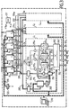
- FIG. 3 shows a diagram of an embodiment of a multiplexing device according to the invention.
- It is composed of a plurality of service circuits C1, C2, ..., C M each provided with an output S1, S2, ..., S M respectively connected to a common data line 200 and a plurality of network circuits R0, R1, R2 and R3, each provided with an input E0, E1, E2 and E3 also connected to this common line 200.
- each of the service circuits C1, C2, ..., C M the terminals 1801 to 1805 for the circuit C1 and the terminals 1806 to 180 N (not shown in FIG. 3 ) for other circuits.
- these circuits C1, C2, ..., C M are each assigned to a given service.
- circuit C1 is assigned to video links such as videoconferencing, circuit C2 to telephone links and circuit C M to extensions of local networks.
- Each circuit C1, C2, ..., C M comprises at least one queue member formed from a memory of the FIFO type (first input data, first output data). This is in practice achieved by means of a random access memory provided with independent read and write circuits.
- We identified by 205 Kohls to 205 P the different queue members contained in the circuit C1.
- These organs make it possible to store different information cells before they pass through the network 100.
- two wires 2061 to 206 P have been assigned on the one hand and 2071 to 207 P , on the other hand, for transmitting respectively a read command signal and an empty memory signal or, in other words, a signal to indicate whether or not the memory contains at least one cell.
- a switching device 250 makes it possible to switch the various access terminals to the queue members 2051 to 205 P.
- This switching member 250 can be coupled to a cell trainer 260 in case these are not formed at the level of the user. This need not be described in more detail since the invention is not concerned with this.
- the commutations carried out by the member 250 are defined by a table 262. This table is registered by means of a management member 270, which can be constituted by an individual computer like PC, to make a correspondence between one of the terminals of access 1801 to 1805 on which a user is connected and one of the queue members 2051 to 205 P.
- a table formed by a memory 275 makes it possible to manage, inside the service circuits, the access of the various queue members to line 200.
- This table also registered from the management member 270, allows to assign a queue member to a destination code being the concatenation of a VPI ("Virtual Path Identifier") and an identifier of the network access point.
- the VPI consists of 8 binary elements and since the number of network accesses is 4 in the example described here, a given destination is therefore represented by a code of 10 binary elements.
- This table is addressed by different destination codes coming from a first service line 280 common to all the service circuits C2, ..., C M. This table provides, in correspondence, the code validating or not a queue organ 205 organe to 205 P.
- a register 288 stores this validation code.
- An OR gate 290 supplies a signal DA1 which, active, signals that at least one queue member of the circuit C1 concerned by the access code contains at least one cell. This is determined by a set of doors ET 2951 to 295 P with two inputs; a first receives the allocation signal from register 288 and the second the signal transmitted by the wires 2071 to 207 P. The inputs of OR gate 290 receive the output signals from gates 2951 to 295 p .
- a decoding circuit 310 provides an active signal when a code corresponding to the identification code of the service circuit is transmitted by a second service line 315.
- the signal decoding from circuit 310 allows the selection of one of the queue members, if there is one concerned by this operation, via a validation circuit 316 which allows the codes contained therein to pass in the register 288 at each edge of a signal H supplied by a clock 317 and therefore activates the reading of the queue member concerned so that a cell is transmitted on the line 200.
- FIG. 4 shows in more detail the structure of the network circuit R0, it being understood that the other circuits R1, R2 and R3 can have the same structure.
- the circuit R0 includes an output circuit 400 which connects the common line 200 to the connection terminal 170.
- It also includes an allocation unit 410 for supplying destination codes at well-defined times.
- the member 410 is provided with an allocation table constituted by a random access memory 412 containing destination codes distributed in a manner which will be explained below and by a table reading member provided for picking up said codes. destination.
- the read member is constituted by an addressing counter 414 of said memory. This counter counts H1 pulses at a fixed rate so that the memory is read cyclically.
- This circuit R0 also includes an arbitration circuit 450.
- This circuit is formed by a processing circuit 455 whose outputs 465 provide the identification code of the service circuit to which access to line 200 has been granted.
- status memory 470 which contains previous states and in particular the identification code of the last service circuit which obtained access for one of the 256 destinations accessible from this network access, the VPI field having 8 binary elements wide.
- the entrees of the processing circuit 455 are constituted, on the one hand, by the signals DA1, DA2, ..., DA M passing through a buffer register 472 and on the other hand by the destination code transmitted on the line 280.
- the information multiplexing device further comprises an allocation member for allocating cell sampling times on said data line 200, to each of the output circuits as a function of the bit rate to be flowed by said output circuits.
- This member is formed from an allocation table in the form of a memory 500 which is addressed by a code of time interval numbers TS transmitted by a line 510 common to all the network circuits R0 , R1, R2 and R3. These time interval codes are produced by a counter 520 (fig. 3) counting the pulses of the signal H.
- the memory 500 is organized in words of a single binary element and has a number of locations equal to the counting capacity of the counter 520. In the context of this example: 64. In the locations of this memory 500, there are allocation indications. Thus, we put a logical "1" to signify that the network circuit is concerned by this time interval code and a "0" to signify that it is not concerned.
- This memory 500 is pre-programmed by means of the management unit 270 in a manner explained below.
- bit rates to be transmitted by the network circuits are low, their number can be multiplied without saturating the transmission capacity of line 200.
- the information multiplexing device described comprises pipeline registers which authorize operation in the pipeline. These different registers are clocked at the rate of the clock signal H.
- pipeline registers 515 and 516 are inserted in the lines of service 280 and 315.
- the other circuits C2 to C M are also obviously equipped with the same registers.
- a first pipeline register 550 interconnects the common data line 200 with the output circuit 400; this register is loaded at the rate of an H5 signal.
- a second register 552 and a third register 553 loaded at the rate of a signal H3 provide the different information to be processed by the arbitration circuit 450.
- register 552 receives the different signals DA1 to DA M and on the other hand the register 553 receives the code transmitted by the service line 280.
- the information produced by this arbitration circuit 450 is received by a fourth register 554 at the rate of a signal H4.
- a fifth register 556 interconnects the output of the allocation unit 410 with the service line 280.
- the signals H2, H3, H4 and H5 are deduced from the signal H1 by successive time offsets each equal to a period of the signal H.
- the signal H1 is derived from the signal H by an AND gate 580 with two inputs, one of which therefore receives the signal H and the other the value of the binary element contained in the memory 500 previously validated. This validation is carried out at the rate of the signal H by means of a flip-flop 582.
- the operation of the information multiplexing device of the invention is as follows.
- This management body 270 is the interface between a management manager who handles this body and the users, on the one hand, and a network manager, on the other hand.
- the manager determines the connections to be made between the various access terminals and the queue members.
- the device manager communicates with the network manager to reserve access with a certain speed.
- the latter provides following this request a destination code representing in a shortened form, as has been said, the destination desired by the recipient. It is from this member that the various table memories 262, 275, 412, 470 and 500 are loaded according to the traffic to be satisfied.
- the cells can be sent over each access link to the network 100 at a maximum rate of 149.76.106 eb / s (binary elements per second).
- the TS time interval codes vary from 0 to 63 and therefore the counter 520 is a modulo 64 counter.
- the network circuits are all called to transmit at this maximum rate, a maximum of 16 TS time codes are allocated among the 64 at each of the network circuits.
- the allocated TS time codes must be separated by at least 3 TS time codes. The period of the signal H is therefore 707.5 ns.
- FIG. 5 shows an example of allocation of these time intervals TS.
- the circuit R0 is assigned to the maximum bit rate, 16 TS codes are allocated to it either: the codes “0", “4", “8", “12", ...
- the circuit R1 is assigned to a bit rate twice as low .
- TS codes "1", “9”, ... are allocated to it.
- the circuit R2 is also assigned to this maximum speed the codes “2", “6", “10", “14”, ..., "62” are allocated to it.
- the circuit R3 is assigned to a slow rate and a single time code TS is allocated to it, ie "4".
- This allocation member 410 defines access times to common line 200 to the queue members contained in the various circuits C1, C2, ..., C M so that cells are emitted on the connection terminal 170 via the common line 200 and the output circuit 400.
- the memory 412 contains destination codes distributed in a manner explained below and the read counter 414 is provided to address this memory at the rate of the signal H1 so that the memory is read continuously in a cyclic manner. This fixes the rate of appearance of said destination codes.
- This memory 412 is also programmed from the management terminal 270.
- a manager takes into account the speed requests for the different destinations and formulates a request to obtain the necessary resources of the network for the envisaged traffic. This request is transferred to the network manager who provides the destination code consisting of a V.P.I. and a code identifying the network access circuit. The manager then writes this destination code into the memory 412 according to the following considerations.
- the frequency of the clock pulses fixes the maximum bit rate that can be transmitted. Either by taking a practical example 149.76.106 eb / s (binary elements per second), so the period for the H1 pulses cannot be less than 2.83 ⁇ s. Thus, if the traffic required for a destination is this maximum speed, all the memory locations will be affected by this service.
- the size of this memory is partly defined by the minimum flow rate d min to be guaranteed, for example: 4.5 103 eb / s.
- the memory size is then 32,768 locations. This size is also defined by the granularity of the bit rates to be transmitted, that is to say the set of different bit rates which can be transmitted. The greater the number of possible debits, the larger the size of the table.
- the memory 470 contains as many memory locations as there are possible VPI codes, namely: 256.
- the arbitration mechanism chosen is that of rotating priority, for each destination, described in "DISTRIBUTED-PROCESSOR COMMUNICATION ARCHITECTURE" by Kenneth J. Thurber, and Gerald M. Masson, published in Lexington Books, Heatch., Chapter 5, pages 140 and 141. Given this mechanism, memory 470 does not require any initialization.
- the priority is determined in several phases of calculations determined by a clock signal H16 which has a frequency sixteen times higher than that of the signals H.
- the arbitration context, for a given destination, is stored in memory 470, at an address deduced from the V.P.I. number. corresponding to this destination.
- a system comprising such a device can be formed from a network of the type shown in FIG. 1. This system then allows the exchange of information between nodes of this network via a device according to the invention.
Abstract
Description
La présente invention concerne un dispositif de multiplexage d'informations pour un réseau du genre A.T.M., notamment, qui transmet d'un de ses points d'accès à un autre des cellules d'informations, dispositif comportant :
- une pluralité de bornes d'accès pour des utilisateurs ayant des informations à transmettre vers une certaine destination avec un certain débit,
- une pluralité de bornes de raccord pour une pluralité de points d'accès dudit réseau,
- une pluralité de circuits de service munis d'organes de files d'attente pour emmagasiner des données d'utilisateur et pour fournir sur des sorties de données les cellules à transmettre,
- une ligne commune de données interconnectant les sorties de données desdits circuits de service,
- une pluralité de circuits de réseau munis de circuits de sortie dont les entrées sont connectées à ladite ligne de données et dont les sorties sont connectées auxdites bornes de raccord.
- a plurality of access terminals for users having information to be transmitted to a certain destination with a certain speed,
- a plurality of connection terminals for a plurality of access points of said network,
- a plurality of service circuits provided with queue members for storing user data and for supplying the cells to be transmitted on data outputs,
- a common data line interconnecting the data outputs of said service circuits,
- a plurality of network circuits provided with output circuits whose inputs are connected to said data line and whose outputs are connected to said connection terminals.
La présente invention concerne également un système comprenant un tel dispositif.The present invention also relates to a system comprising such a device.
Les réseaux A.T.M. se répandent de plus en plus et pour les utiliser au maximum des possibilités qu'ils offrent, il convient de multiplexer les données que l'utilisateur veut transmettre.The A.T.M. are spreading more and more and to use them to the maximum of the possibilities which they offer, it is advisable to multiplex the data which the user wants to transmit.
Un dispositif de ce genre qui peut effectuer des opérations de multiplexage est connu de la demande de brevet n° 2 670 972.A device of this kind which can carry out multiplexing operations is known from patent application No. 2 670 972.
Ce dispositif connu est formé de joncteurs d'entrée dont les fonctions peuvent être assimilées aux circuits de service précités et des joncteurs de sortie assimilables aux circuits de réseau.This known device is formed of input junctions whose functions can be assimilated to the circuits of aforementioned service and output trunks comparable to network circuits.
Tous les joncteurs, tant de sortie que d'entrée, doivent avoir des caractéristiques identiques puisqu'on doit effectuer des opérations de brassages pour lesquelles toute cellule à l'entrée de n'importe quel joncteur d'entrée peut aller à la sortie de n'importe quel joncteur de sortie. Cependant, en ce qui concerne les opérations de multiplexage, les utilisateurs pour se connecter à un réseau A.T.M. peuvent utiliser des liaisons qui assurent des débits différents : fibres optiques, lignes téléphoniques... Le dispositif connu ne donne aucune mesure spéciale pour adapter les joncteurs de sortie au débit offert par la liaison à laquelle ils sont connectés. Il en découle qu'il faut prévoir des files d'attente au niveau des joncteurs de sortie afin d'absorber, pour une part, ces variations de débit.All trunks, both output and input, must have identical characteristics since it is necessary to carry out patching operations for which any cell at the input of any input trunk can go to the output of n any output trunk. However, with respect to multiplexing operations, users to connect to an A.T.M. can use links which provide different bit rates: optical fibers, telephone lines ... The known device does not give any special measure to adapt the output trunks to the bit rate offered by the link to which they are connected. It follows that it is necessary to provide queues at the output junctions in order to absorb, in part, these variations in flow.
La présente invention propose un dispositif qui permet donc d'adapter les circuits de réseaux au débit de la liaison à laquelle ils sont reliés et qui ne nécessite pas forcément, au niveau des circuits de réseau, de files d'attente et de moyens de gestion qui doivent leur être associés.The present invention provides a device which therefore makes it possible to adapt the network circuits to the speed of the link to which they are connected and which does not necessarily require, at the level of the network circuits, queues and management means. which must be associated with them.
Pour cela, un tel dispositif est remarquable en ce qu'il comporte en outre :
- un organe d'allocation pour allouer des temps de prélèvement de cellules sur ladite ligne de données à chacun des circuits de sortie en fonction du débit à écouler par lesdits circuits de sortie.
- an allocation member for allocating cell sampling times on said data line to each of the output circuits as a function of the flow rate to be flowed through said output circuits.
La description suivante, accompagnée des dessins ci-annexés, le tout donné à titre d'exemple non limitatif, fera bien comprendre comment l'invention peut être réalisée.
- La figure 1 montre un réseau sur lequel est connecté un dispositif de multiplexage conforme à l'invention.
- La figure 2 montre la structure des cellules d'information transmises par le réseau.
- La figure 3 montre un dispositif de multiplexage conforme à l'invention.
- La figure 4 montre un circuit de réseau faisant partie du dispositif de la figure 3.
- La figure 5 montre un diagramme temps montrant le fonctionnement en pipe-line du dispositif de l'invention.
- FIG. 1 shows a network to which a multiplexing device according to the invention is connected.
- Figure 2 shows the structure of the information cells transmitted by the network.
- Figure 3 shows a multiplexing device according to the invention.
- FIG. 4 shows a network circuit forming part of the device of FIG. 3.
- Figure 5 shows a time diagram showing the pipeline operation of the device of the invention.
La figure 1 montre d'une manière schématisée un réseau A.T.M. portant sur la figure la référence 100. On trouvera une description de ce réseau dans l'ouvrage
" ASYNCHRONOUS TRANSFER MODE " de MARTIN de PRYCKER paru aux éditions ELLIS HORWOOD en Angleterre. Ce réseau est constitué de différents noeuds 102, 103, 104, 105, 106, 107 et 108 reliés entre eux par des liaisons 110 à 118 pour relier respectivement les noeuds 102-103, 102-107, 103-105, 103-104, 104-105, 104-108, 104-106, 107-108 et 106-107. On a repéré par 120 à 128 différents points d'accès de ce réseau. Ces points d'accès sont respectivement reliés aux noeuds 108, 106, 107, 102, 103 et 105 par l'intermédiaire de liaisons 130 à 138 respectivement. A ces points d'accès, se connectent différents dispositifs de multiplexage et de démultiplexage 160, 161 et 162. Parmi ces dispositifs, il faut distinguer : un dispositif de multiplexage 160, objet de la présente invention, et deux dispositifs de démultiplexage 161 et 162 qui effectuent les opérations inverses de celles du dispositif 160. Pour être relié aux quatre points 120, 121, 122 et 123, le dispositif de multiplexage 160 est muni de quatre bornes de raccord 170, 171, 172 et 173. Ainsi les informations peuvent, dans le cadre de cet exemple décrit, aller du dispositif 160 vers les dispositifs 162 et 164 en transitant par le réseau 100. Ces informations à transmettre sont appliquées à une pluralité de bornes d'accès 180₁ à 180N dont est pourvu le dispositif de multiplexage 160, et peuvent être fournies, entre autres, a des bornes de sortie 185₁ à 185N' du dispositif 161 et 190₁ à 190N'' du dispositif 162. Les informations transmises dans le réseau se présentent sous forme de cellules dont l'allure est montrée à la figure 2. Ces cellules sont formées de 53 octets : 5 constituent l'entête HD et les 48 autres PL contiennent les données pour un service à transmettre accompagnées éventuellement d'informations supplémentaires pour reconstituer les données de ce service à la réception.Figure 1 shows schematically an ATM network with the
"ASYNCHRONOUS TRANSFER MODE" by MARTIN de PRYCKER published by ELLIS HORWOOD editions in England. This network is made up of
La figure 3 montre un schéma de réalisation d'un dispositif de multiplexage conforme à l'invention.FIG. 3 shows a diagram of an embodiment of a multiplexing device according to the invention.
Il est composé d'une pluralité de circuits de service C₁, C₂, ..., CM munis chacun d'une sortie S₁, S₂, ..., SM respectivement reliée à une ligne de données commune 200 et d'une pluralité de circuits de réseau R₀, R₁, R₂ et R₃, munis chacun d'une entrée E₀, E₁, E₂ et E₃ reliée aussi à cette ligne commune 200.It is composed of a plurality of service circuits C₁, C₂, ..., C M each provided with an output S₁, S₂, ..., S M respectively connected to a
A chacun des circuits de service C₁, C₂, ..., CM sont rattachées des bornes d'accès d'utilisateurs : les bornes 180₁ à 180₅ pour le circuit C₁ et les bornes 180₆ à 180N (non représentées sur la figure 3) pour les autres circuits. En principe, ces circuits C₁, C₂, ..., CM sont chacun affectés à un service donné. Par exemple, le circuit C₁ est affecté aux liaisons vidéo genre vidéoconférence, le circuit C₂ aux liaisons téléphoniques et le circuit CM à des prolongations de réseaux locaux.User access terminals are attached to each of the service circuits C₁, C₂, ..., C M : the
Chaque circuit C₁, C₂, ..., CM comporte au moins un organe de file d'attente formé à partir d'une mémoire du genre F.I.F.O (première donnée entrée, première donnée sortie). Ceci est en pratique réalisé au moyen d'une mémoire vive munie de circuits de lecture et d'écriture indépendants. On a repéré par 205₁ à 205P les différents organes de file d'attente contenus dans le circuit C₁. Ces organes permettent de stocker différentes cellules d'informations avant leur passage au travers du réseau 100. Pour chacun de ces organes, on a affecté deux fils 206₁ à 206P d'une part et 207₁ à 207P, d'autre part, pour transmettre respectivement un signal de commande de lecture et un signal de mémoire vide ou, en d'autres termes, un signal pour indiquer si la mémoire contient ou non au moins une cellule. Un organe de commutation 250 permet de commuter les différentes bornes d'accès sur les organes de file d'attente 205₁ à 205P. Cet organe de commutation 250 peut être couplé à un formateur de cellules 260 au cas où celles-ci ne seraient pas formées au niveau de l'utilisateur. Ceci n'a pas besoin d'être décrit plus en détail car l'invention n'est pas concernée par cela. Les commutations effectuées par l'organe 250 sont définies par une table 262. Cette table est inscrite au moyen d'un organe de gestion 270, qui peut être constitué par un ordinateur individuel genre PC, pour faire une correspondance entre une des bornes d'accès 180₁ à 180₅ sur laquelle un utilisateur est connecté et un des organes de files d'attente 205₁ à 205P.Each circuit C₁, C₂, ..., C M comprises at least one queue member formed from a memory of the FIFO type (first input data, first output data). This is in practice achieved by means of a random access memory provided with independent read and write circuits. We identified by 205 contenus to 205 P the different queue members contained in the circuit C₁. These organs make it possible to store different information cells before they pass through the
Une table formée par une mémoire 275 permet de gérer à l'intérieur des circuits de service l'accès des différents organes de file d'attente à la ligne 200. Cette table, inscrite aussi à partir de l'organe de gestion 270, permet d'affecter un organe de file d'attente à un code de destination étant la concaténation d'un V.P.I. ("Virtual Path Identifier") et d'un identificateur du point d'accès réseau. Le V.P.I. est constitué de 8 éléments binaires et comme le nombre d'accès réseau est de 4 dans l'exemple décrit ici, une destination donnée est donc représentée par un code de 10 éléments binaires. Cette table est adressée par différents codes de destination provenant d'une première ligne de service 280 commune à tous les circuits de service C₂, ..., CM. Cette table fournit, en correspondance, le code validant ou non un organe de file d'attente 205₁ à 205P. Un registre 288 emmagasine ce code de validation. Une porte OU 290 fournit un signal DA1 qui, actif, signale qu'au moins un organe de file d'attente du circuit C1 concerné par le code d'accès contient au moins une cellule. Ceci est déterminé par un ensemble de portes ET 295₁ à 295P à deux entrées ; une première reçoit le signal d'affectation provenant du registre 288 et la seconde le signal transmis par les fils 207₁ à 207P. Les entrées de la porte OU 290 reçoivent les signaux de sortie des portes 295₁ à 295p.A table formed by a
Comme chaque circuit de service est affecté d'un code d'identification, un circuit de décodage 310 fournit un signal actif lorsqu'un code correspondant au code d'identification du circuit de service est transmis par une deuxième ligne de service 315. Le signal de décodage issu du circuit 310 permet la sélection d'un des organes de file d'attente, s'il y en a un de concerné par cette opération, par l'intermédiaire d'un circuit de validation 316 qui laisse passer les codes contenus dans le registre 288 à chaque front d'un signal H fourni par une horloge 317 et de ce fait, active la lecture de l'organe de file d'attente concerné pour qu'une cellule soit émise sur la ligne 200.As each service circuit is assigned an identification code, a decoding circuit 310 provides an active signal when a code corresponding to the identification code of the service circuit is transmitted by a
La figure 4 montre plus en détail la structure du circuit de réseau R0, étant entendu que les autres circuits R1, R2 et R3 peuvent avoir la même structure.FIG. 4 shows in more detail the structure of the network circuit R0, it being understood that the other circuits R1, R2 and R3 can have the same structure.
Le circuit R0 comporte un circuit de sortie 400 qui relie la ligne commune 200 à la borne de raccord 170.The circuit R0 includes an
Il comporte aussi un organe d'affectation 410 pour fournir des codes de destination en des temps bien définis.It also includes an allocation unit 410 for supplying destination codes at well-defined times.
L'organe 410 est muni d'une table d'affectation constituée par une mémoire vive 412 contenant des codes de destination répartis d'une manière qui sera explicitée ci-dessous et d'un organe de lecture de table prévu pour prélever lesdits codes de destination. L'organe de lecture est constitué par un compteur d'adressage 414 de ladite mémoire. Ce compteur compte des impulsions H1 à cadence fixe de sorte que la mémoire est lue d'une manière cyclique.The member 410 is provided with an allocation table constituted by a
Ce circuit R0 comporte encore un circuit d'arbitrage 450. Ce circuit est formé d'un circuit de traitement 455 dont les sorties 465 fournissent le code d'identification du circuit de service auquel on a accordé l'accès à la ligne 200. Une mémoire de statut 470 qui contient des états antérieurs et notamment le code d'identification du dernier circuit de service qui a obtenu l'accès pour une des 256 destinations accessibles à partir de cet accès réseau, le champ V.P.I. ayant 8 éléments binaires de large. Les entrées du circuit de traitement 455 sont constitués, d'une part, par les signaux DA1, DA2, ..., DAM transitant par un registre tampon 472 et d'autre part par le code de destination transmis sur la ligne 280.This circuit R0 also includes an
Conformément à l'invention, le dispositif de multiplexage d'informations comporte, en outre, un organe d'allocation pour allouer des temps de prélèvement de cellules sur ladite ligne de données 200, à chacun des circuits de sortie en fonction du débit à écouler par lesdits circuits de sortie. Cet organe est constitué à partir d'une table d'allocation se présentant sous la forme d'une mémoire 500 qui est adressée par un code de numéros d'intervalle de temps TS transmis par une ligne 510 commune à tous les circuits de réseau R0, R1, R2 et R3. Ces codes d'intervalle de temps sont élaborés par un compteur 520 (fig. 3) comptant les impulsions du signal H.According to the invention, the information multiplexing device further comprises an allocation member for allocating cell sampling times on said
La mémoire 500 est organisée en mots d'un seul élément binaire et a un nombre d'emplacements égal à la capacité de comptage du compteur 520. Dans le cadre de cet exemple : 64. Dans les emplacements de cette mémoire 500, on dispose des indications d'allocation. Ainsi, on met un "1" logique pour signifier que le circuit de réseau est concerné par ce code d'intervalle de temps et un "0" pour signifier qu'il n'est pas concerné. Cette mémoire 500 est pré-programmée au moyen de l'organe de gestion 270 d'une manière explicitée ci-dessous.The
Si les débits à transmettre par les circuits de réseau sont faibles, on peut multiplier leur nombre sans saturer la capacité de transmission de la ligne 200.If the bit rates to be transmitted by the network circuits are low, their number can be multiplied without saturating the transmission capacity of
Conformément à un autre aspect de l'invention, le dispositif de multiplexage d'information décrit comporte des registres de pipe-line qui autorisent un fonctionnement en pipe-line. Ces différents registres sont cadencés au rythme du signal d'horloge H.In accordance with another aspect of the invention, the information multiplexing device described comprises pipeline registers which authorize operation in the pipeline. These different registers are clocked at the rate of the clock signal H.
Sur le circuit de service C₁, des registres de pipe-line 515 et 516 sont insérés dans les lignes de service 280 et 315. Les autres circuits C₂ à CM sont aussi évidemment équipés des mêmes registres.On the service circuit C₁, pipeline registers 515 and 516 are inserted in the lines of
Sur le circuit de réseau R0, un premier registre de pipe-line 550 interconnecte la ligne de données commune 200 avec le circuit de sortie 400 ; ce registre est chargé au rythme d'un signal H5. Un deuxième registre 552 et un troisième registre 553 chargé au rythme d'un signal H3 fournissent les différentes informations à traiter par le circuit d'arbitrage 450. D'une part le registre 552 reçoit les différents signaux DA₁ à DAM et d'autre part le registre 553 reçoit le code transmis par la ligne de service 280. L'information élaborée par ce circuit d'arbitrage 450 est reçue par un quatrième registre 554 au rythme d'un signal H4. Un cinquième registre 556 interconnecte la sortie de l'organe d'affectation 410 avec la ligne de service 280.On the network circuit R0, a first pipeline register 550 interconnects the
Les signaux H2, H3, H4 et H5 se déduisent du signal H1 par des décalages temporels successifs égaux chacun à une période du signal H. Le signal H1 est dérivé du signal H par une porte ET 580 à deux entrées dont une reçoit donc le signal H et l'autre la valeur de l'élément binaire contenu dans la mémoire 500 préalablement validé. Cette validation est effectuée au rythme du signal H au moyen d'une bascule 582.The signals H2, H3, H4 and H5 are deduced from the signal H1 by successive time offsets each equal to a period of the signal H. The signal H1 is derived from the signal H by an AND
Des éléments de retard 590, 591, 592 et 593 montés en cascade à la sortie de la porte 580 fournissent respectivement les signaux H2 à H5. Ces éléments de retard apportent un retard égal à la période citée ci-dessus.Delay
Le fonctionnement du dispositif de multiplexage d'informations de l'invention est le suivant.The operation of the information multiplexing device of the invention is as follows.
Cet organe de gestion 270 est l'interface entre un gestionnaire de gestion qui manipule cet organe et les utilisateurs, d'une part, et un gestionnaire de réseau, d'autre part.This
Le gestionnaire détermine les connexions à faire entre les différentes bornes d'accès et les organes de file d'attente. Le gestionnaire du dispositif communique avec le gestionnaire du réseau pour réserver un accès avec un certain débit. Ce dernier fournit à la suite de cette demande un code de destination représentant sous une forme raccourcie, ainsi qu'il l'a été dit, la destination voulue par le destinataire. C'est à partir de cet organe que les différentes mémoires tables 262, 275, 412, 470 et 500 sont chargées en fonction du trafic à satisfaire.The manager determines the connections to be made between the various access terminals and the queue members. The device manager communicates with the network manager to reserve access with a certain speed. The latter provides following this request a destination code representing in a shortened form, as has been said, the destination desired by the recipient. It is from this member that the
Dans le cadre de l'exemple décrit les cellules peuvent être envoyées sur chaque lien d'accès au réseau 100 à un rythme maximal de 149,76.10⁶ eb/s (éléments binaires par seconde). Les codes d'intervalle de temps TS varient de 0 à 63 et de ce fait le compteur 520 est un compteur modulo 64. Comme les circuits de réseau sont tous appelés à transmettre avec ce rythme maximal, on alloue au maximum 16 codes de temps TS parmi les 64 à chacun des circuits de réseau. Pour un même circuit de réseau, les codes de temps TS alloués doivent être séparés d'au moins 3 codes de temps TS. La période du signal H est donc de 707,5 ns.In the context of the example described, the cells can be sent over each access link to the
A la figure 5, on a représenté un exemple d'allocation de ces intervalles de temps TS. Ainsi le circuit R0 est affecté au débit maximal, 16 codes TS lui sont alloués soit : les codes "0", "4", "8", "12", ... Le circuit R1 est affecté à un débit deux fois moindre. Les codes TS "1", "9", ... lui sont alloués. Le circuit R2 est affecté lui aussi à ce débit maximal les codes "2", "6", "10", "14", ..., "62" lui sont alloués. Le circuit R3 est affecté à un débit lent et un seul code de temps TS lui est alloué soit "4".FIG. 5 shows an example of allocation of these time intervals TS. Thus the circuit R0 is assigned to the maximum bit rate, 16 TS codes are allocated to it either: the codes "0", "4", "8", "12", ... The circuit R1 is assigned to a bit rate twice as low . TS codes "1", "9", ... are allocated to it. The circuit R2 is also assigned to this maximum speed the codes "2", "6", "10", "14", ..., "62" are allocated to it. The circuit R3 is assigned to a slow rate and a single time code TS is allocated to it, ie "4".
Cet organe d'affectation 410 définit des temps d'accès à ligne commune 200 aux organes de file d'attente contenus dans les différents circuits C₁, C₂, ..., CM pour que des cellules soient émises sur la borne de raccord 170 via la ligne commune 200 et le circuit de sortie 400. La mémoire 412 contient des codes de destination répartis d'une manière explicitée ci-dessous et le compteur de lecture 414 est prévu pour adresser cette mémoire à la cadence du signal H1 de sorte que la mémoire est lue en permanence d'une manière cyclique. Ceci fixe la cadence d'apparition desdits codes de destination.This allocation member 410 defines access times to
Cette mémoire 412 est programmée également à partir du terminal de gestion 270. Un gestionnaire prend en compte les demandes de débit pour les différentes destinations et formule une demande pour obtenir les ressources nécessaires du réseau pour le trafic envisagé. Cette demande est transférée au gestionnaire du réseau qui fournit le code de destination constitué d'un V.P.I. et d'un code identifiant le circuit d'accès réseau. Le gestionnaire inscrit ensuite ce code de destination dans la mémoire 412 en fonction des considérations suivantes.This
La fréquence des impulsions d'horloge fixe le débit maximal susceptible d'être transmis. Soit en prenant un exemple pratique 149,76.10⁶ eb/s (éléments binaires par seconde), donc la période pour les impulsions H1 ne peut pas être inférieure à 2,83 µs. Ainsi, si le trafic exigé pour une destination est ce débit maximal, tous les emplacements de la mémoire seront concernés par ce service. La taille de cette mémoire est définie en partie par le débit minimal dmin à assurer par exemple : 4,5 10³ eb/s. La taille de la mémoire est alors de 32 768 emplacements. Cette taille est aussi définie par la granularité des débits à transmettre, c'est-à-dire l'ensemble des débits différents que l'on peut transmettre. Plus le nombre de débits possibles est grand, plus la taille de la table sera grande.The frequency of the clock pulses fixes the maximum bit rate that can be transmitted. Either by taking a practical example 149.76.10⁶ eb / s (binary elements per second), so the period for the H1 pulses cannot be less than 2.83 µs. Thus, if the traffic required for a destination is this maximum speed, all the memory locations will be affected by this service. The size of this memory is partly defined by the minimum flow rate d min to be guaranteed, for example: 4.5 10³ eb / s. The memory size is then 32,768 locations. This size is also defined by the granularity of the bit rates to be transmitted, that is to say the set of different bit rates which can be transmitted. The greater the number of possible debits, the larger the size of the table.
La mémoire 470 contient autant d'emplacements mémoires qu'il y a de codes V.P.I. possibles soit : 256. Le mécanisme d'arbitrage choisi est celui de la priorité tournante, pour chacune des destination, décrite dans
" DISTRIBUTED-PROCESSOR COMMUNICATION ARCHITECTURE " de Kenneth J. Thurber, et Gerald M. Masson, paru dans Lexington Books, Heatch., Chapitre 5, pages 140 et 141. Etant donné ce mécanisme, la mémoire 470 ne nécessite aucune initialisation.The memory 470 contains as many memory locations as there are possible VPI codes, namely: 256. The arbitration mechanism chosen is that of rotating priority, for each destination, described in
"DISTRIBUTED-PROCESSOR COMMUNICATION ARCHITECTURE" by Kenneth J. Thurber, and Gerald M. Masson, published in Lexington Books, Heatch.,
La priorité est déterminée en plusieurs phases de calculs déterminées par un signal d'horloge H16 qui a une fréquence seize fois plus élevée que celle des signaux H.The priority is determined in several phases of calculations determined by a clock signal H16 which has a frequency sixteen times higher than that of the signals H.
Le contexte d'arbitrage, pour une destination donnée, est stocké dans la mémoire 470, à une adresse déduite du numéro de V.P.I. correspondant à cette destination.The arbitration context, for a given destination, is stored in memory 470, at an address deduced from the V.P.I. number. corresponding to this destination.
Une séquence d'arbitrage se décompose alors selon les phases suivantes :
- on prélève dans la mémoire 470 le contexte d'arbitrage relatif au code de destination V.P.I.,
- on réalise l'arbitrage entre les différents circuits d'accès, selon le mécanisme de priorité tournante,
- on émet sur la ligne 315 le code du circuit qui a gagné l'accès,
- on enregistre dans la mémoire 470 le nouveau contexte d'arbitrage relatif au code de destination V.P.I.
- the arbitration context relating to the destination code VPI is taken from memory 470,
- arbitration is carried out between the different access circuits, according to the rotating priority mechanism,
- the code of the circuit which gained access is sent on
line 315, - the new arbitration context relating to the VPI destination code is stored in memory 470
La figure 5 illustre bien ce fonctionnement.Figure 5 illustrates this well.
Lorsque TS = "0", un élément binaire de valeur "1" est présent à la sortie de la bascule 582 du circuit de réseau, ce qui fait apparaître le signal H1. C'est la phase d'allocation.When TS = "0", a binary element of value "1" is present at the output of flip-
Lorsque TS = "1", le code de destination provenant de la mémoire 412 du circuit de réseau est émis sur la ligne de service 280. C'est la phase d'appel pour une destination.When TS = "1", the destination code from
Ce code est analysé au niveau de chaque circuit de service au moyen de la mémoire 275. Si un des organes de file d'attente est concerné par cette destination le signal DA1 est actif. Les signaux DA₁ à DAM provenant de tous les circuits de service sont analysés par le circuit de réseau R0 lorsque TS = "2". C'est la phase de demande d'accès de la ligne de données.This code is analyzed at each service circuit by means of
Le circuit d'arbitrage du circuit de réseau R0 donne son verdict lorsque TS = "3". C'est la phase d'accord pour un accès à la ligne commune.The arbitration circuit of the network circuit R0 gives its verdict when TS = "3". This is the agreement phase for access to the common line.
Lorsque TS = "4", la cellule de l'organe de file d'attente concerné est émise sur la ligne de données. C'est la phase d'émission de données.When TS = "4", the cell of the queue member concerned is sent on the data line. This is the data transmission phase.
Un système comprenant un tel dispositif peut être formé à partir d'un réseau du type montré à la figure 1. Ce système permet alors l'échange d'informations entre des noeuds de ce réseau via un dispositif conforme à l'invention.A system comprising such a device can be formed from a network of the type shown in FIG. 1. This system then allows the exchange of information between nodes of this network via a device according to the invention.
Claims (7)
Applications Claiming Priority (2)
| Application Number | Priority Date | Filing Date | Title |
|---|---|---|---|
| FR9303776 | 1993-03-31 | ||
| FR9303776 | 1993-03-31 |
Publications (1)
| Publication Number | Publication Date |
|---|---|
| EP0618748A1 true EP0618748A1 (en) | 1994-10-05 |
Family
ID=9445585
Family Applications (1)
| Application Number | Title | Priority Date | Filing Date |
|---|---|---|---|
| EP94200810A Withdrawn EP0618748A1 (en) | 1993-03-31 | 1994-03-25 | Apparatus and system for information multiplexing in ATM network |
Country Status (3)
| Country | Link |
|---|---|
| US (1) | US5539738A (en) |
| EP (1) | EP0618748A1 (en) |
| JP (1) | JPH07183895A (en) |
Cited By (2)
| Publication number | Priority date | Publication date | Assignee | Title |
|---|---|---|---|---|
| EP0735793A1 (en) * | 1995-03-29 | 1996-10-02 | Philips Communication D'entreprise | Communication system including a network and a multiplexer |
| EP0771130A1 (en) | 1995-10-25 | 1997-05-02 | Philips Communication D'entreprise | Multiplexing and scheduling apparatus for an ATM switching network |
Families Citing this family (3)
| Publication number | Priority date | Publication date | Assignee | Title |
|---|---|---|---|---|
| JP3437071B2 (en) * | 1997-10-28 | 2003-08-18 | 富士通株式会社 | ATM cell multiplexer |
| JP3679249B2 (en) * | 1998-07-31 | 2005-08-03 | 富士通株式会社 | ATM cell multiplexer |
| FR2823037B1 (en) * | 2001-03-27 | 2003-06-20 | Thomson Csf | METHOD FOR OPTIMIZING THE MANAGEMENT OF THE BANDWIDTH OF A DIGITAL TRANSMISSION CHANNEL |
Citations (3)
| Publication number | Priority date | Publication date | Assignee | Title |
|---|---|---|---|---|
| EP0138717A2 (en) * | 1983-10-14 | 1985-04-24 | Denis Chomel | Asynchronous digital time-multiplex system with a distributed bus |
| EP0351014A2 (en) * | 1988-07-14 | 1990-01-17 | Philips Patentverwaltung GmbH | Switching network for a switching system |
| FR2670972A1 (en) * | 1990-12-20 | 1992-06-26 | Lmt Radio Professionelle | TRANSIT SWITCH OF AN ASYNCHRONOUS NETWORK, IN PARTICULAR AN ATM NETWORK. |
Family Cites Families (4)
| Publication number | Priority date | Publication date | Assignee | Title |
|---|---|---|---|---|
| US4597075A (en) * | 1981-08-21 | 1986-06-24 | Italtel-Societa Italiana Telecomunicazioni S.P.A. | Modular switching network for telecommunication system |
| FR2635243B1 (en) * | 1988-08-05 | 1994-01-14 | Lmt Radio Professionnelle | PACKET SWITCHER FOR ASYNCHRONOUS DATA TRANSFER IN A DIGITAL TRANSMISSION NETWORK |
| US5072442A (en) * | 1990-02-28 | 1991-12-10 | Harris Corporation | Multiple clock rate teleconferencing network |
| US5251209A (en) * | 1991-03-28 | 1993-10-05 | Sprint International Communications Corp. | Prioritizing attributes in integrated services networks |
-
1994
- 1994-03-25 EP EP94200810A patent/EP0618748A1/en not_active Withdrawn
- 1994-03-30 US US08/221,149 patent/US5539738A/en not_active Expired - Fee Related
- 1994-03-31 JP JP6293294A patent/JPH07183895A/en active Pending
Patent Citations (3)
| Publication number | Priority date | Publication date | Assignee | Title |
|---|---|---|---|---|
| EP0138717A2 (en) * | 1983-10-14 | 1985-04-24 | Denis Chomel | Asynchronous digital time-multiplex system with a distributed bus |
| EP0351014A2 (en) * | 1988-07-14 | 1990-01-17 | Philips Patentverwaltung GmbH | Switching network for a switching system |
| FR2670972A1 (en) * | 1990-12-20 | 1992-06-26 | Lmt Radio Professionelle | TRANSIT SWITCH OF AN ASYNCHRONOUS NETWORK, IN PARTICULAR AN ATM NETWORK. |
Non-Patent Citations (1)
| Title |
|---|
| B. VOETEN ET AL, INT. SWITCHING SYMPOSIUM90, vol. 6, May 1990 (1990-05-01), SWEDEN, pages 25 - 28, XP000130957 * |
Cited By (3)
| Publication number | Priority date | Publication date | Assignee | Title |
|---|---|---|---|---|
| EP0735793A1 (en) * | 1995-03-29 | 1996-10-02 | Philips Communication D'entreprise | Communication system including a network and a multiplexer |
| FR2732530A1 (en) * | 1995-03-29 | 1996-10-04 | Trt Telecom Radio Electr | COMMUNICATION SYSTEM COMPRISING A NETWORK AND MULTIPLEXING DEVICE SUITABLE FOR SUCH A SYSTEM |
| EP0771130A1 (en) | 1995-10-25 | 1997-05-02 | Philips Communication D'entreprise | Multiplexing and scheduling apparatus for an ATM switching network |
Also Published As
| Publication number | Publication date |
|---|---|
| JPH07183895A (en) | 1995-07-21 |
| US5539738A (en) | 1996-07-23 |
Similar Documents
| Publication | Publication Date | Title |
|---|---|---|
| EP0618749A1 (en) | Apparatus and system for information multiplexing in ATM network | |
| EP0293315B1 (en) | Method and system for controlling the flow of data packets | |
| CA2050405C (en) | Temporary information storage system incorporating a buffer memory for fixed or variable length data blocks | |
| EP1507374B1 (en) | Method and device for priority management during a message transmission. | |
| EP0126196B1 (en) | Asynchronous time-division switching network for point-to-point, merging and broadcast communications | |
| FR2694828A1 (en) | Packet transfer computer bus. | |
| FR2617304A1 (en) | PROGRAMMABLE INPUT / OUTPUT SEQUENCER FOR INPUT / OUTPUT PROCESSOR | |
| FR2701180A1 (en) | Cellulization device and device for decellulising synchronous digital channels, synchronous digital channel switching center, and asynchronous digital channel switching center. | |
| EP0383660B1 (en) | Rate reservation in an asynchronous packet network | |
| EP0920157A1 (en) | Device for managing a shared buffer memory | |
| FR2549673A1 (en) | Elementary switch for automatic switching unit using an asynchronous multiplexing technique. | |
| FR2824434A1 (en) | Digital packet switched network broadcasting nodes/links having nodes broadcasting simultaneously several links and recovery path calculation minimising links per node. | |
| EP0020255B1 (en) | Switching level of an operator for a packet-switched digital data network | |
| EP0618748A1 (en) | Apparatus and system for information multiplexing in ATM network | |
| EP0406077A1 (en) | Complementary connectionless communication system for asynchronous time network | |
| EP0689371A1 (en) | Communication system having a network and multiplexing unit | |
| EP0612172A1 (en) | Opto-electronic satellite centre for connecting optical subscriber-lines to an ATM network | |
| EP0771130B1 (en) | Multiplexing and scheduling apparatus for an ATM switching network | |
| EP0899917B1 (en) | Aparatus and method for group switching ATM cells with corresponding terminating functionality at the input and output | |
| EP0114433B1 (en) | Telephone switching system | |
| EP0632669B1 (en) | Communication system including ATM network and demultiplexer | |
| EP0652662B1 (en) | Waiting queues arrangement to be used at the input stage of a non-blocking space-switching matrix | |
| FR2758427A1 (en) | SWITCHING ELEMENT, IN PARTICULAR ATM CELLS, USING PROBABILISTIC PRIORITIES ATTACHED TO CELLS | |
| FR2721416A1 (en) | Device for routing asynchronous transfer mode data cells. | |
| EP0675618A1 (en) | Adapting device between a time synchronous network and a time asynchronous network |
Legal Events
| Date | Code | Title | Description |
|---|---|---|---|
| PUAI | Public reference made under article 153(3) epc to a published international application that has entered the european phase |
Free format text: ORIGINAL CODE: 0009012 |
|
| AK | Designated contracting states |
Kind code of ref document: A1 Designated state(s): DE FR GB |
|
| 17P | Request for examination filed |
Effective date: 19950405 |
|
| RAP1 | Party data changed (applicant data changed or rights of an application transferred) |
Owner name: PHILIPS ELECTRONICS N.V. Owner name: PHILIPS COMMUNICATION D'ENTREPRISE |
|
| RAP1 | Party data changed (applicant data changed or rights of an application transferred) |
Owner name: COMPAGNIE DES SIGNAUX Owner name: PCE |
|
| RAP1 | Party data changed (applicant data changed or rights of an application transferred) |
Owner name: CS COMMUNICATION & SYSTEMES Owner name: PCE |
|
| STAA | Information on the status of an ep patent application or granted ep patent |
Free format text: STATUS: THE APPLICATION HAS BEEN WITHDRAWN |
|
| 18W | Application withdrawn |
Withdrawal date: 20020323 |