EP0618698A1 - Optical means for clock recovery of a coded signal - Google Patents
Optical means for clock recovery of a coded signal Download PDFInfo
- Publication number
- EP0618698A1 EP0618698A1 EP94400645A EP94400645A EP0618698A1 EP 0618698 A1 EP0618698 A1 EP 0618698A1 EP 94400645 A EP94400645 A EP 94400645A EP 94400645 A EP94400645 A EP 94400645A EP 0618698 A1 EP0618698 A1 EP 0618698A1
- Authority
- EP
- European Patent Office
- Prior art keywords
- signal
- circuit
- optical
- coded signal
- coded
- Prior art date
- Legal status (The legal status is an assumption and is not a legal conclusion. Google has not performed a legal analysis and makes no representation as to the accuracy of the status listed.)
- Withdrawn
Links
Images

Classifications
-
- H—ELECTRICITY
- H04—ELECTRIC COMMUNICATION TECHNIQUE
- H04L—TRANSMISSION OF DIGITAL INFORMATION, e.g. TELEGRAPHIC COMMUNICATION
- H04L7/00—Arrangements for synchronising receiver with transmitter
- H04L7/0075—Arrangements for synchronising receiver with transmitter with photonic or optical means
Definitions
- the subject of the present invention is an optical device making it possible to recover the rhythm (also called a clock) of a signal coded by a digital code. It finds numerous applications in the field of digital transmission by optical fibers.
- the object of the present invention is precisely to remedy this drawback. To this end, it offers an optical device for recovering the clock of signals coded according to different digital codes such as the NRZ (No Return to Zero) code where each information bit at "1" has a duration of a period clock, CMI code (Code Mark Inversion) where the information bits are coded alternately "01" and "10", the biphase code, etc ...
- NRZ No Return to Zero
- CMI code Code Mark Inversion
- the interferometer is a MACH-ZEHNDER interferometer, made of optical fibers.
- the circuit for shaping the coded signal comprises an AM / FM converter associated in series with the interferometer, to convert the amplitude modulated signal into a frequency modulated signal.
- This AM / FM converter is preferably a laser converter.
- An optical filter can, moreover, be associated in series with the AM / FM converter, and be adjusted to one of the frequencies of the frequency modulated signal to ensure the establishment of a logic function, the choice of the logic function to establish dependent on the digital code of the coded signal.
- the rhythm recovery circuit comprises a two-to-two coupler making it possible to introduce the pulses coming from the circuit for shaping the coded signal and to carry out the feedback loop.
- the two-to-two coupler is made of optical fibers.
- the rhythm recovery circuit includes an amplifier and an optical filter associated in series in the feedback loop.
- the rhythm recovery device can include an optical equalizer connected to the second output of the recovery circuit.
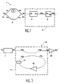
- FIG 1 there is shown schematically the circuit for shaping the coded signal received by the device according to the invention.
- This circuit for shaping the coded signal is referenced 1; we will therefore write indifferently, in the following description, circuit 1 and circuit for shaping the coded signal.
- This circuit for shaping the coded signal includes an interferometer 3.
- the signal coded according to any one of the known digital codes is introduced into the shaping circuit. by input 3a of the interferometer 3.
- This signal coded by a digital code, also called initial signal, is referenced Si.
- This signal Si is therefore injected into the interferometer 3, which is preferably a MACH interferometer -ZEHNDER.
- This MACH-ZEHNDER interferometer has the advantage of being easily achievable in optical fibers.
- the interferometer 3 is made of optical fibers so as to allow the continuity of the propagation of the signal If transmitted to device 1 by fiber optic links.
- the signal Si when it is introduced into the interferometer 3, is able to follow two paths, namely the path Ta and the path Tb.
- the delay R between the two paths that is to say the path difference between the paths Ta and Tb, is substantially equal to T / 2.
- the signals used in the interferometer for the path Ta and for the path Tb are, respectively, referenced Sa and Sb. These signals Sa and Sb are shown in Figure 3 attached which will be described in more detail in the following description.
- These signals Sa and Sb are offset by about half a period T / 2 by the interferometer.
- the signal Sc obtained at the output 3b of the interferometer 3 is the signal resulting from the signals Sa and Sb.
- This optical signal Sc then has three amplitude levels, A1, A2, A3, as shown in FIG. 3.
- R N x T / 2> rx Lc
- N is an integer
- T is the propagation time of the signals in the fiber (approximately 5 ns / m)
- the signal Sc obtained at the output of the interferometer 3 is injected into a generator 9 of optical logic functions.
- This generator includes a 5 AM / FM converter associated with an optical filter.
- the converter 5 makes it possible in particular to convert the amplitude modulated signals from the interferometer 3 into frequency modulated signals.
- This converter 5 is preferably of the laser type.
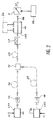
- An embodiment of the generator 9 of logic functions is represented in FIG. 2. This generator of logic functions is capable of supplying at its output a logic function, in optical form, which is reconfigurable, that is to say that the 'We can choose this logic function among several logic functions achievable with this generator.
- this generator uses an optical transposition in a distributed feedback laser diode which it comprises, as well as an optical filter 7 tunable in frequency.
- a distributed feedback laser diode which it comprises, as well as an optical filter 7 tunable in frequency.
- Such an optical transposition is described in the document: "Wavenlength conversion for FM light using light injection induced frequency shift in DFB-LD", by K INOUE and N. TAKATO, published in Electronics Letters, 28 September 1989, vol. 25, n ° 20, p. 1360-62.
- the laser diode LD1 at the output of which an optical isolator 14 is placed, is connected by an optical fiber 16 to an input of the optical coupler 10.
- the laser diode LD2 at the output of which an optical isolator 18 is placed, is connected by an optical fiber 20 to the other input of the optical coupler 10.
- the light capable of being supplied by the output of the optical coupler 10 is sent to the laser diode LD3 via an optical fiber 22 and injected into the active layer of this laser diode LD3.
- the LD3 laser diode which has two polarization electrodes, is provided with control means 24 provided to send respectively to these electrodes two constant polarization currents, chosen so that the LD3 laser diode is single mode and provides a beam output. laser 26.
- the wavelength of the output light beam 26 is the quiescent wavelength LO of the laser diode LD3.
- the optical frequency corresponding to this wavelength LO is denoted F1.
- the optical filter 7, which is frequency tunable, is placed at the output of the laser diode LD3 and intended to select an optical frequency from the optical frequencies of the light signals capable of being supplied by the laser diode LD3.
- This optical filter 7 can be controlled by appropriate means 28.
- the laser diodes LD1 and LD2 are respectively controlled by the signal Sc from the interferometer 3.
- the laser diodes LD1 and LD2 being controlled by the same signal, they respectively emit digital optical signals S1 and S2 which are synchronous and have the same bit rate.
- optical signals are mixed by the optical coupler 10 and are injected simultaneously into the active layer of the laser diode LD3.
- a polarization controller CP is placed at the input of the laser diode LD3 in order to give the signals S1 and S2 leaving the optical fiber 22 a direction of polarization situated in the plane of polarization of the laser diode LD3 ( plane of the active layer of this LD3 laser diode).
- Each of the optical signals S1 and S2 is a series of high levels (logic levels 1) and low levels (logic levels 0).
- the light power injected into the LD3 laser diode varies over time.
- the light power injected into the laser diode LD3 is zero.
- the optical frequency of the light beam 26 emitted by this laser diode LD3 is the quiescent frequency FO of the laser diode LD3.
- the light power injected into this laser diode LD3 is not zero and the frequency of the light signal supplied by the laser diode LD3 slides to a value F2 greater than F1.
- the light power injected into the laser diode LD3 is the maximum light power that can be obtained with the signals S1 and S2.
- the optical frequency of the light signal 26 supplied by the laser diode LD3 slides, in this case c), up to a value F3 greater than F2.
- the digital optical signal Sd which is obtained at the output of the optical filter 7 tunable in frequency is a function of what the optical filter has selected as frequency: the frequency F1, the frequency F2 or the frequency F3.
- optical filter 7 makes it possible to select one of the three logical functions AND (AND in the articles in English language), NON AND (NAND in the articles in English language) and EXCLUSIVE OR (XOR in the articles in English language) .
- the digital optical signal Sd supplied by the optical filter 7 corresponds to the NAND logic function.
- this digital optical signal Sd corresponds to the logic function OR EXCLUSIVE.
- this digital optical signal Sd corresponds to the logic function AND.
- This frequency-tunable optical filter 7 can be a tunable Perot Fabry interferometer.
- the frequency tunable optical filter 7 is constituted by an auxiliary laser diode with distributed feedback which is polarized below its threshold current by appropriate means.
- This auxiliary laser diode has two polarization electrodes and it is by adjusting the value of the polarization currents respectively supplied by appropriate means that the value of the frequency selected by this auxiliary laser diode forming the optical filter is chosen.
- the signal Sd supplied on the output 5b of the converter 5 is therefore a frequency modulated signal on three frequencies F1, F2, F3, the temporal duration of the states of which has not been modified.
- This signal Sd is then introduced into the optical filter 7 by the input 7a of said filter which is connected to the output 5b of the converter 5.
- This optical filter can, for example, be adjusted to the frequency F2 so that the generator 9 of functions logic establishes the OU-EXCLUSIVE function.
- the optical logic function to be established is the OR-EXCLUSIVE function.
- This OR-EXCLUSIVE function is carried out by adjusting the optical filter 7 on the frequency F2 of the signal SD introduced into said optical filter 7.
- the generator 9 of logic functions can establish the AND logic function in order to recover the clock of a signal coded by a two-phase code.
- the signal Se supplied by the output 7b of the filter 7 meets the conditions necessary to allow the implementation of the circuit for recovering the rhythm of the coded signal. These conditions are, as has been given previously, that the signal Se which is a series of pulses, has pulses of duration equal to the half clock period T / 2 and of variable occurrence equal to N x T, where the coefficient N is a time-varying integer whose maximum value depends essentially on the code of the coded signal introduced in circuit 1.
- FIG. 3 the circuit for recovering the rhythm of the coded signal is shown diagrammatically. This rhythm recovery circuit is referenced 19; we will therefore talk about circuit 19.
- This rhythm recovery circuit 19 is connected to the output 7b of the circuit 1 for shaping the coded signal.
- This circuit 19 includes a 2 to 2 coupler.
- this coupler is made of optical fibers, so as to allow continuity of the propagation of the optical signal Se obtained at the output of the shaping circuit 1.
- This 2 to 2 coupler referenced 11 in FIG. 3, has a first and a second input, respectively 11a and 11b, and a first and a second output, respectively 11c and 11d.
- the input 11a receives the signal from the output of the shaping circuit 1.
- This signal is referenced Sf in FIG. 3; it corresponds to the signal Se of FIG. 1; it however carries a different reference so as to ensure consistency between the signals Sf and Sg of FIG. 3 which are represented, in FIG. 4, in a time reference different from the signal referenced Se.
- the output 11d of the clock recovery circuit 11 provides the signal Sg corresponding to the sought clock signal.
- the output 11c of the coupler 11 is connected to the input 11b of this coupler, in order to produce a feedback loop.
- An amplifier 13 and an optical filter 15 are connected in series with each other in the feedback loop, that is to say that they are connected after the output 11c and before the input 11b of the coupler. This association of the amplifier 13 and the optical filter 15 has the advantage of making it possible to adjust the length of the feedback loop, so that the propagation time of the optical signal in said feedback loop is equal to the period T of the clock that one seeks to recover.
- an optical equalizer 17 is connected to the output 11d of the coupler 11.
- This optical equalizer 17 is, according to one embodiment, an optical amplifier similar to the amplifier 13 used in the feedback loop.
- the non-linearity of the gain curve of this amplifier 17, when it operates in saturation, makes it possible to correct the amplitude variation of the pulses of the signal Sg.
- the signal obtained at the output of this optical equalizer 17 is referenced Sg '.
- optical amplifiers 13 and 17 of the semiconductor optical amplifier type are used, the propagation time of which is less than 5 pins / second.
- FIG 4 there is shown the different signals obtained during processing by the device of the invention.
- the signal represented in A is the signal Sa which is one of the signals of the two paths of the interferometer 3.
- the signal Sb is the signal obtained for the second path of the interferometer 3.
- This signal Sb, represented in B is shifted by half-period with respect to the signal shown in A.
- This half-period T / 2 is equivalent to the delay R allocated by the interferometer 3 on the signal flowing in the path Tb with respect to the signal flowing in the path Ta.
- these signals Sa and Sb, represented respectively at A and B are substantially identical to the coded signal Si but shifted in time by half a period for the signal Sb.
- the signal shown in C that is to say the signal Sc obtained at the output of the interferometer 3, is a signal resulting from the sum of the signals Sa and Sb.
- This signal Sc is an amplitude modulated signal according to three levels A1, A2, A3, as shown in FIG. 4.
- the signal Sd represented at D in FIG. 43 shows the signal obtained at the output of the converter 5, that is to say that it shows the frequency modulated signal.
- This signal Sd has three frequency levels, F1, F2, F3; the states of this signal Sd are identical from the time duration point of view to those of the signal Sc amplitude modulated.
- the signal Se represented at E in FIG. 4 shows the signal obtained at the output of circuit 1 for shaping the coded signal.
- This signal Se is the signal obtained after adjustment on the frequency F2 by the optical filter 7.
- This signal Se is therefore frequency modulated according to two levels, F1 and F2.
- the signals Sf and Sg represented at F and at G correspond to the signals which are at the input and at the output of the circuit 11 for clock recovery.
- the signal Sf represented at F represents the same signal as the signal Se, but in a time frame different from that of Se. Indeed, the signals represented in F and G illustrate the signals which one would obtain on an oscillator placed in entry and exit of the circuit 19 clock recovery. Thus, the signal Sf illustrates the pulses obtained at the output of the circuit 1 for shaping the coded signal.
- the signal Sg represented in G, shows the clock signal obtained at the output of the coupler 11, that is to say the clock signal sought.
Abstract
Description
La présente invention a pour objet un dispositif optique permettant de récupérer le rythme (que l'on appelle aussi horloge) d'un signal codé par un code numérique. Elle trouve de nombreuses applications dans le domaine de la transmission numérique par fibres optiques.The subject of the present invention is an optical device making it possible to recover the rhythm (also called a clock) of a signal coded by a digital code. It finds numerous applications in the field of digital transmission by optical fibers.
Dans la plupart des systèmes de transmission numérique, il est nécessaire de pouvoir resynchroniser, à sa réception, le signal d'information transmis sous forme numérique afin de lire l'information qu'il contient. De nombreux dispositifs électroniques pouvant récupérer l'horloge du signal d'information (c'est-à-dire l'horloge du signal codé qu'ils reçoivent) sont connus. Cependant, lorsque le système de transmission est de type optique (transmission par fibres optiques), il est souvent important d'assurer la continuité optique dans le système. Un dispositif optique de récupération de l'horloge doit alors être utilisé.In most digital transmission systems, it is necessary to be able to resynchronize, on reception, the information signal transmitted in digital form in order to read the information that it contains. Numerous electronic devices capable of recovering the clock of the information signal (that is to say the clock of the coded signal which they receive) are known. However, when the transmission system is of the optical type (transmission by optical fibers), it is often important to ensure optical continuity in the system. An optical clock recovery device must then be used.
Le document de D.J. AS, R. EGGEMANN et al. intitulé "Clock revery based on a new type of selfpulsation in a 1,5 µm two-section InGaAsP-InP DFB laser", publié dans Electronics Letters, 21st January 1991, vol. 29, n° 2, décrit un tel dispositif optique de récupération d'horloge. Ce dispositif, qui utilise des diodes laser à contre-réaction, a pour principal inconvénient de ne permettre la récupération d'horloge qu'à partir de signaux codés par le code RZ (Retour à Zéro) pour lequel chaque bit d'information (bit à l'état "1") du signal a une durée équivalant à une demi-période d'horloge.The document by DJ AS, R. EGGEMANN et al. entitled "Clock revery based on a new type of selfpulsation in a 1.5 µm two-section InGaAsP-InP DFB laser", published in Electronics Letters, 21st January 1991, vol. 29, n ° 2, describes such an optical device clock recovery. The main drawback of this device, which uses feedback laser diodes, is to allow clock recovery only from signals coded by the code RZ (Return to Zero) for which each bit of information (bit in state "1") of the signal has a duration equivalent to half a clock period.
La présente invention a justement pour but de remédier à cet inconvénient. A cette fin, elle propose un dispositif optique de récupération de l'horloge de signaux codés selon différents codes numériques tels que le code NRZ (Non Retour à Zéro) où chaque bit d'information à "1" a une durée d'une période d'horloge, le code CMI (Code Mark Inversion) où les bits d'infomation sont codé alternativement "01" et "10", le code biphase, etc...The object of the present invention is precisely to remedy this drawback. To this end, it offers an optical device for recovering the clock of signals coded according to different digital codes such as the NRZ (No Return to Zero) code where each information bit at "1" has a duration of a period clock, CMI code (Code Mark Inversion) where the information bits are coded alternately "01" and "10", the biphase code, etc ...
Afin de permettre la récupération d'horloge de signaux pouvant être codés selon une multitude de codes numériques, le dispositif de l'invention comporte, en amont du circuit de récupération du rythme, un circuit de mise en forme du signal codé reçu. Ce circuit de mise en forme transcrit le signal codé sous la forme d'une série d'implusions répondant aux conditions suivantes :
- les impulsions ont une durée égale à une demi-période d'horloge (T/2);
- les impulsions ont une occurence variable, égale à NxT, où N est un nombre entier variant en fonction du code numérique utilisé pour coder le signal codé. De façon plus précise, l'invention concerne un dispositif optique de récupération du rythme d'un signal codé par un code numérique et transmis audit dispositif au moyen de liaisons en fibres optiques pour fournir un signal de rythme. Ce dispositif comporte :
- un circuit de mise en forme du signal codé apte à transcrire ledit signal codé sous la forme d'une série d'impulsions de durée égale à N x T/2, où T est la période du rythme du signal codé et N est un nombre entier variant en fonction du code numérique codant le signal codé, et d'occurence égale à NxT, ce circuit comportant une entrée apte à recevoir le signal codé et une sortie apte à fournir la série d'impulsions ; et
- Un circuit de récupération du rythme qui comprend une première et une seconde entrées et une première et une seconde sorties, la première entrée étant connectée sur la sortie du circuit de mise en forme et la première sortie étant connectée sur la seconde entrée pour former une boucle de contre-réaction ; ce circuit de récupération du rythme est apte, de plus, à déterminer, pour chaque période du rythme, une fraction du signal se propageant dans la boucle de contre-réaction pour fournir, sur la seconde sortie, cette fraction de signal correspondant au signal de rythme.
- the pulses have a duration equal to half a clock period (T / 2);
- the pulses have a variable occurrence, equal to NxT, where N is an integer varying according to the digital code used to code the coded signal. More specifically, the invention relates to an optical device for recovering the rhythm of a signal coded by a digital code and transmitted to said device by means of fiber optic links for providing a timing signal. This device includes:
- a circuit for shaping the coded signal capable of transcribing said coded signal in the form of a series of pulses of duration equal to N x T / 2, where T is the period of the rhythm of the coded signal and N is a number integer varying as a function of the digital code encoding the coded signal, and of occurrence equal to NxT, this circuit comprising an input capable of receiving the coded signal and an output capable of supplying the series of pulses; and
- A rhythm recovery circuit which includes first and second inputs and first and second outputs, the first input being connected to the output of the shaping circuit and the first output being connected to the second input to form a loop feedback; this rhythm recovery circuit is further capable of determining, for each period of the rhythm, a fraction of the signal propagating in the feedback loop to provide, on the second output, this fraction of signal corresponding to the signal of rhythm.
Avantageusement, le circuit de mise en forme du signal codé comporte un interféromètre de retard R = N x T/2 pour transformer le signal codé en un signal modulé en amplitude.Advantageously, the circuit for shaping the coded signal comprises a delay interferometer R = N x T / 2 for transforming the coded signal into an amplitude modulated signal.
De préférence, l'interféromètre est un interféromètre de MACH-ZEHNDER, réalisé en fibres optiques.Preferably, the interferometer is a MACH-ZEHNDER interferometer, made of optical fibers.
Selon l'invention, le circuit de mise en forme du signal codé comporte un convertisseur AM/FM associé en série à l'interféromètre, pour convertir le signal modulé en amplitude en un signal modulé en fréquence.According to the invention, the circuit for shaping the coded signal comprises an AM / FM converter associated in series with the interferometer, to convert the amplitude modulated signal into a frequency modulated signal.
Ce convertisseur AM/FM est, de préférence, un convertisseur laser.This AM / FM converter is preferably a laser converter.
Un filtre optique peut, en outre, être associé en série au convertisseur AM/FM, et être ajusté sur l'une des fréquences du signal modulé en fréquence pour assurer l'établissement d'une fonction logique, le choix de la fonction logique à établir dépendant du code numérique du signal codé.An optical filter can, moreover, be associated in series with the AM / FM converter, and be adjusted to one of the frequencies of the frequency modulated signal to ensure the establishment of a logic function, the choice of the logic function to establish dependent on the digital code of the coded signal.
Selon un mode de réalisation préféré de l'invention, le circuit de récupération du rythme comporte un coupleur deux vers deux permettant d'introduire les impulsions provenant du circuit de mise en forme du signal codé et de réaliser la boucle de contre-réaction.According to a preferred embodiment of the invention, the rhythm recovery circuit comprises a two-to-two coupler making it possible to introduce the pulses coming from the circuit for shaping the coded signal and to carry out the feedback loop.
De préférence, le coupleur deux vers deux est réalisé en fibres optiques.Preferably, the two-to-two coupler is made of optical fibers.
De façon avantageuse, le circuit de récupération du rythme comporte un amplificateur et un filtre optique associés en série dans la boucle de contre-réaction.Advantageously, the rhythm recovery circuit includes an amplifier and an optical filter associated in series in the feedback loop.
Selon une caractéristique de l'invention, le dispositif de récupération de rythme peut comporter un égaliseur optique connecté sur la seconde sortie du circuit de récupération.According to a characteristic of the invention, the rhythm recovery device can include an optical equalizer connected to the second output of the recovery circuit.
- La figure 1 représente, de façon schématique, le circuit de mise en forme du signal codé ;FIG. 1 schematically represents the circuit for shaping the coded signal;
- la figure 2 représente un mode de réalisation du générateur de fonctions logiques ;FIG. 2 represents an embodiment of the generator of logic functions;
- la figure 3 représente schématiquement le circuit de récupération de rythme connecté en sortie du circuit de mise en forme ;FIG. 3 schematically represents the rhythm recovery circuit connected at the output of the shaping circuit;
- la figure 4 illustre les différents signaux obtenus au cours du traitement par le dispositif de l'invention : A et B représentent les signaux utilisés par l'interféromètre ; C, le signal modulé en amplitude sur trois niveaux ; D, le signal modulé en fréquence ; E, le signal modulé en amplitude sur deux niveaux ; F, montre les impulsions obtenues en sortie du circuit de mise en forme ; et G, le signal de rythme.FIG. 4 illustrates the different signals obtained during processing by the device of the invention: A and B represent the signals used by the interferometer; C, the amplitude modulated signal on three levels; D, the frequency modulated signal; E, the amplitude modulated signal on two levels; F, shows the pulses obtained at the output of the shaping circuit; and G, the rhythm signal.
Sur la figure 1, on a représenté schématiquement le circuit de mise en forme du signal codé reçu par le dispositif selon l'invention. Ce circuit de mise en forme du signal codé est référencé 1 ; on écrira donc indifféremment, dans la suite de la description, circuit 1 et circuit de mise en forme du signal codé.In Figure 1, there is shown schematically the circuit for shaping the coded signal received by the device according to the invention. This circuit for shaping the coded signal is referenced 1; we will therefore write indifferently, in the following description,
Ce circuit de mise en forme du signal codé comporte un interféromètre 3. Le signal codé selon l'un quelconque des codes numériques connus (codes RZ, NRZ, CMI, Biphase, etc...) est introduit dans le circuit de mise en forme par l'entrée 3a de l'interféromètre 3. Ce signal codé par un code numérique, appelé également signal initial, est référencé Si. Ce signal Si est donc injecté dans l'interféromètre 3, qui est, de préférence, un interféromètre de MACH-ZEHNDER. Cet interféromètre de MACH-ZEHNDER a pour avantage d'être facilement réalisable en fibres optiques. Aussi, selon le mode de réalisation préféré de l'invention, l'interféromètre 3 est réalisé en fibres optiques de façon à permettre la continuité de la propagation du signal Si transmis au dispositif 1 par des liaisons en fibres optiques.This circuit for shaping the coded signal includes an
Le signal Si, lorsqu'il est introduit dans l'interféromètre 3, est apte à suivre deux trajets, à savoir le trajet Ta et le trajet Tb. Le retard R entre les deux trajets, c'est-à-dire la différence de marche entre les trajets Ta et Tb, est égale à sensiblement T/2. Les signaux utilisés dans l'interféromètre pour le trajet Ta et pour le trajet Tb sont, respectivement, référencés Sa et Sb. Ces signaux Sa et Sb sont représentés sur la figure 3 ci-jointe que l'on décrira plus en détail dans la suite de la description. Ces signaux Sa et Sb sont décalés d'environ une demi-période T/2 par l'interféromètre. De cette façon, le signal Sc obtenu à la sortie 3b de l'interféromètre 3 est le signal résultant des signaux Sa et Sb. Ce signal optique Sc comporte alors trois niveaux d'amplitude, A1, A2, A3, comme cela est montré sur la figure 3.The signal Si, when it is introduced into the
Cependant, afin d'éviter toute interférence, c'est-à-dire tout battement optique des deux signaux Sa et Sb en sortie, il est préférable d'augmenter le retard R de façon à ce que :![]()
où N est un nombre entier, T est le temps de propagation des signaux dans la fibre (sensiblement de 5 ns/m) et Lc est la longueur de cohérence de la porteuse optique avec![]()
où λ est la longueur d'onde de la porteuse optique,
δλ est l'encombrement spectral,
c est la vitesse de la lumière,
δ![]()
n est l'indice du milieu de propagation.However, in order to avoid any interference, that is to say any optical beating of the two signals Sa and Sb at the output, it is preferable to increase the delay R so that: ![]()
where N is an integer, T is the propagation time of the signals in the fiber (approximately 5 ns / m) and Lc is the coherence length of the optical carrier with ![]()
where λ is the wavelength of the optical carrier,
δλ is the spectral congestion,
c is the speed of light,
δ ![]()
n is the index of the propagation medium.
Le signal Sc obtenu à la sortie de l'interféromètre 3 est injecté dans un générateur 9 de fonctions logiques optiques. Ce générateur comporte un convertisseur 5 AM/FM associé à un filtre optique. Le convertisseur 5 permet notamment de convertir les signaux modulés en amplitude provenant de l'interféromètre 3 en des signaux modulés en fréquence. Ce convertisseur 5 est, de préférence, de type laser. Un mode de réalisatin du générateur 9 de fonctions logiques est représenté sur la figure 2. Ce générateur de fonctions logiques est capable de fournir à sa sortie une fonction logique, sous forme optique, qui est reconfigurable, c'est-à-dire que l'on peut choisir cette fonction logique parmi plusieurs fonctions logiques réalisables avec ce générateur.The signal Sc obtained at the output of the
Pour ce faire, ce générateur utilise une transposition optique dans une diode laser à contre-réaction distribuée qu'il comporte, ainsi qu'un filtre optique 7 accordable en fréquence. Une telle transposition optique est décrite dans le document :"Wavenlength conversion for FM light using light injection induced frequency shift in DFB-LD", de K INOUE et N. TAKATO, publié dans Electronics Letters, 28 September 1989, vol. 25, n° 20, p. 1360-62.To do this, this generator uses an optical transposition in a distributed feedback laser diode which it comprises, as well as an
On a représenté schématiquement, sur la figure 2, un mode de réalisation particulier de ce générateur de fonctions logiques. Il comprend :
- deux diodes lasers monomodes LD1 et LD2,
- un coupleur optique 10 à deux entrées et une sortie (coupleur de type "2
vers 1"), - une diode laser à contre-réaction distribuée LD3, et
un filtre optique 7 qui est accordable en fréquence.
- two single-mode laser diodes LD1 and LD2,
- an
optical coupler 10 with two inputs and one output ("2 to 1" type coupler), - a LD3 distributed feedback laser diode, and
- an
optical filter 7 which is frequency tunable.
La diode laser LD1, à la sortie de laquelle est placé un isolateur optique 14, est reliée par une fibre optique 16 à une entrée du coupleur optique 10.The laser diode LD1, at the output of which an
De même, la diode laser LD2, à la sortie de laquelle est placé un isolateur optique 18, est reliée par une fibre optique 20 à l'autre entrée du coupleur optique 10.Likewise, the laser diode LD2, at the output of which an
La lumière susceptible d'être fournie par la sortie du coupleur optique 10 est envoyée à la diode laser LD3 par l'intermédiaire d'une fibre optique 22 et injectée dans la couche active de cette diode laser LD3.The light capable of being supplied by the output of the
La diode laser LD3, qui comporte deux électrodes de polarisation, est munie de moyens de commande 24 prévus pour envoyer respectivement à ces électrodes deux courants de polarisation constants, choisis de façon à ce que la diode laser LD3 soit monomode et fournisse en sortie un faisceau laser 26.The LD3 laser diode, which has two polarization electrodes, is provided with control means 24 provided to send respectively to these electrodes two constant polarization currents, chosen so that the LD3 laser diode is single mode and provides a beam output.
A la place de la diode laser LD3 à deux électrodes, on pourraît utiliser une diode laser à contre-réaction distribuée à une seule électrode de polarisation, mais il faudrait alors lui faire subir un traitement anti-reflet pour la rendre monomode (au cas où elle ne le serait pas).Instead of the LD3 laser diode with two electrodes, one could use a laser feedback diode distributed with a single polarization electrode, but it would then have to be subjected to an anti-reflection treatment to make it single mode (in the case where it would not be).
Tant que la diode laser LD3 ne reçoit aucun signal lumineux en provenance du coupleur optique 10, la longueur d'onde du faisceau lumineux de sortie 26 est la longueur d'onde de repos LO de la diode laser LD3.As long as the laser diode LD3 receives no light signal from the
La fréquence optique correspondant à cette longueur d'onde LO est notée F1.The optical frequency corresponding to this wavelength LO is denoted F1.
Le filtre optique 7, qui est accordable en fréquence, est placé à la sortie de la diode laser LD3 et prévu pour sélectionner une fréquence optique parmi les fréquences optiques des signaux lumineux susceptibles d'être fournis par la diode laser LD3.The
Ce filtre optique 7 peut être commandé par des moyens appropriés 28.This
Les diodes lasers LD1 et LD2 sont respectivement commandées par le signal Sc provenant de l'interféromètre 3.The laser diodes LD1 and LD2 are respectively controlled by the signal Sc from the
Les diodes lasers LD1 et LD2 étant commandées par un même signal, elles émettent respectivement des signaux optiques numériques S1 et S2 qui sont synchrones et ont le même débit.The laser diodes LD1 and LD2 being controlled by the same signal, they respectively emit digital optical signals S1 and S2 which are synchronous and have the same bit rate.
Ces signaux optiques sont mélangés par le coupleur optique 10 et sont injectés simultanément dans la couche active de la diode laser LD3.These optical signals are mixed by the
On précise qu'un contrôleur de polarisation CP est placé à l'entrée de la diode laser LD3 afin de donner aux signaux S1 et S2 sortant de la fibre optique 22 une direction de polarisation située dans le plan de polarisation de la diode laser LD3 (plan de la couche active de cette diode laser LD3).It is specified that a polarization controller CP is placed at the input of the laser diode LD3 in order to give the signals S1 and S2 leaving the optical fiber 22 a direction of polarization situated in the plane of polarization of the laser diode LD3 ( plane of the active layer of this LD3 laser diode).
Chacun des signaux optiques S1 et S2 est une suite de niveaux hauts (niveaux logiques 1) et de niveaux bas (niveaux logiques 0).Each of the optical signals S1 and S2 is a series of high levels (logic levels 1) and low levels (logic levels 0).
La puissance lumineuse injectée dans la diode laser LD3 varie au cours du temps.The light power injected into the LD3 laser diode varies over time.
Trois cas se présentent :
- a) deux niveaux logiques 0, provenant respectivement des diodes lasers LD1 et LD2, arrivent simultanément sur la diode laser LD3,
- b) un niveau logique 0, provenant de l'une des diodes lasers LD1 et LD2, et
un niveau logique 1, provenant de l'autre de ces diodes lasers LD1 et LD2, arrivent simultanément sur la diode laser LD3, et - c) deux niveaux logiques 1, provenant respectivement des diodes lasers LD1 et LD2, arrivent simultanément sur la diode laser LD3.
- a) two logic levels 0, coming respectively from the laser diodes LD1 and LD2, arrive simultaneously on the laser diode LD3,
- b) a logic level 0, coming from one of the laser diodes LD1 and LD2, and a
logic level 1, coming from the other of these laser diodes LD1 and LD2, arrive simultaneously on the laser diode LD3, and - c) two
logic levels 1, coming respectively from the laser diodes LD1 and LD2, arrive simultaneously on the laser diode LD3.
Dans le cas a), la puissance lumineuse injectée dans la diode laser LD3 est nulle.In case a), the light power injected into the laser diode LD3 is zero.
En conséquence, la fréquence optique du faisceau lumineux 26 émis par cette diode laser LD3 est la fréquence de repos FO de la diode laser LD3.Consequently, the optical frequency of the
Dans le cas b), la puissance lumineuse injectée dans cette diode laser LD3 n'est pas nulle et la fréquence du signal lumineux fourni par la diode laser LD3 glisse jusqu'à une valeur F2 supérieure à F1.In case b), the light power injected into this laser diode LD3 is not zero and the frequency of the light signal supplied by the laser diode LD3 slides to a value F2 greater than F1.
Enfin, dans le cas c), la puissance lumineuse injectée dans la diode laser LD3 est la puissance lumineuse maximale que l'on puisse obtenir avec les signaux S1 et S2.Finally, in case c), the light power injected into the laser diode LD3 is the maximum light power that can be obtained with the signals S1 and S2.
La fréquence optique du signal lumineux 26 fourni par la diode laser LD3 glisse, dans ce cas c), jusqu'à une valeur F3 supérieure à F2.The optical frequency of the
On obtient donc, à la sortie de la diode laser LD3, un signal optique numérique dont la fréquence optique passe successivement de l'une des valeurs F1, F2 et F3 à une autre de ces valeurs au cours d'un temps t.There is therefore obtained, at the output of the laser diode LD3, a digital optical signal whose optical frequency passes successively from one of the values F1, F2 and F3 to another of these values during a time t.
Ainsi, le signal optique numérique Sd que l'on obtient à la sortie du filtre optique 7 accordable en fréquence est fonction de ce que le filtre optique a sélectionné comme fréquence : la fréquence F1, la fréquence F2 ou la fréquence F3.Thus, the digital optical signal Sd which is obtained at the output of the
Aussi, le filtre optique 7 permet de sélectionner l'une des trois fonctions logiques ET (AND dans les articles en langue anglaise), NON ET (NAND dans les articles en langue anglaise) et OU EXCLUSIF (XOR dans les articles en langue anglaise).Also, the
Plus précisément, lorsque la fréquence F1 est sélectionnée, le signal optique numérique Sd fourni par le filtre optique 7 correspond à la fonction logique NON ET.More precisely, when the frequency F1 is selected, the digital optical signal Sd supplied by the
Lorsque la fréquence F2 est sélectionnée, ce signal optique numérique Sd correspond à la fonction logique OU EXCLUSIF.When the frequency F2 is selected, this digital optical signal Sd corresponds to the logic function OR EXCLUSIVE.
Enfin, lorsque la fréquence F3 est sélectionnée ce signal optique numérique Sd correspond à la fonction logique ET.Finally, when the frequency F3 is selected, this digital optical signal Sd corresponds to the logic function AND.
On dispose ainsi d'un générateur de fonctions logiques optiques qui est remarquable par le fait que cette fonction logique est reconfigurable, c'est-à-dire peut être choisie parmi plusieurs fonctions logiques suivant la fréquence optique sélectionnée par le filtre optique accordable en fréquence 7.There is thus a generator of optical logical functions which is remarkable in that this logical function is reconfigurable, that is to say can be chosen from several logical functions according to the optical frequency selected by the optical filter tunable in frequency. 7.
Ce filtre optique 7 accordable en fréquence peut être un interféromètre de Perot Fabry accordable.This frequency-tunable
Dans un autre mode de réalisation particulier, le filtre optique accordable en fréquence 7 est constitué par une diode laser auxiliaire à contre-réaction distribuée qui est polarisée au-dessous de son courant de seuil par des moyens appropriés.In another particular embodiment, the frequency tunable
Cette diode laser auxiliaire comporte deux électrodes de polarisation et c'est en règlant la valeur des courants de polarisation respectivement fournis par des moyens appropriés que l'on choisit la valeur de la fréquence sélectionnée par cette diode laser auxiliaire formant le filtre optique.This auxiliary laser diode has two polarization electrodes and it is by adjusting the value of the polarization currents respectively supplied by appropriate means that the value of the frequency selected by this auxiliary laser diode forming the optical filter is chosen.
Au sujet d'une telle diode laser formant un filtre optique on pourra par exemple consulter le document suivant :
Demande de brevet français n° 90 06 926 du 5 juin 1990, "Système de transmission bidirectionnelle à composants lasers identiques". On the subject of such a laser diode forming an optical filter, we can for example consult the following document:
French patent application No. 90 06 926 of June 5 , 1990, "Bidirectional transmission system with identical laser components".
Le signal Sd fourni sur la sortie 5b du convertisseur 5 est donc un signal modulé en fréquence sur trois fréquences F1, F2, F3, dont la durée temporelle des états n'a pas subi de modifications.The signal Sd supplied on the
Ce signal Sd est alors introduit dans le filtre optique 7 par l'entrée 7a dudit filtre qui est connecté sur la sortie 5b du convertisseur 5. Ce filtre optique peut, par exemple, être ajusté sur la fréquence F2 afin que le générateur 9 de fonctions logiques établisse la fonction OU-EXCLUSIF.This signal Sd is then introduced into the
Selon une application de ce dispositif de l'invention, on cherche à récupérer l'horloge à partir d'un signal codé par le code NRZ. Pour récupérer l'horloge d'un tel signal, la fonction logique optique à établir est la fonction OU-EXCLUSIF. Cette fonction OU-EXCLUSIF est réalisée en ajustant le filtre optique 7 sur la fréquence F2 du signal SD introduit dans ledit filtre optique 7.According to an application of this device of the invention, it is sought to recover the clock from a signal coded by the NRZ code. To recover the clock of such a signal, the optical logic function to be established is the OR-EXCLUSIVE function. This OR-EXCLUSIVE function is carried out by adjusting the
Selon un autre exemple, le générateur 9 de fonctions logiques peut établir la fonction logique ET afin de récupérer l'horloge d'un signal codé par un code biphase.According to another example, the
Aussi, le signal Se fourni par la sortie 7b du filtre 7 répond aux conditions nécessaires pour permettre la mise en oeuvre du circuit de récupération du rythme du signal codé. Ces conditions sont, comme cela a été donné précédemment, que le signal Se qui est une série d'impulsions, ait des impulsions de durée égale à la demi-période horloge T/2 et d'occurence variable égale N x T, où le coefficient N est un nombre entier variable dans le temps et dont la valeur maximale dépend essentiellement du code du signal codé introduit dans le circuit 1.Also, the signal Se supplied by the output 7b of the
Sur la figure 3, on a représenté schématiquement le circuit de récupération du rythme du signal codé. Ce circuit de récupération du rythme est référencé 19 ; on parlera donc du circuit 19.In FIG. 3, the circuit for recovering the rhythm of the coded signal is shown diagrammatically. This rhythm recovery circuit is referenced 19; we will therefore talk about
Ce circuit 19 de récupération du rythme est connecté sur la sortie 7b du circuit 1 de mise en forme du signal codé. Ce circuit 19 comporte un coupleur 2 vers 2. Préférentiellement, ce coupleur est réalisé en fibres optiques, de façon à permettre la continuité de la propagation du signal optique Se obtenu en sortie du circuit 1 de mise en forme.This
Ce coupleur 2 vers 2, référencé 11 sur la figure 3, comporte une première et une seconde entrée, respectivement 11a et 11b, et une première et une seconde sortie, respectivement 11c et 11d. L'entrée 11a reçoit le signal provenant de la sortie du circuit 1 de mise en forme.This 2 to 2 coupler, referenced 11 in FIG. 3, has a first and a second input, respectively 11a and 11b, and a first and a second output, respectively 11c and 11d. The
Ce signal est référencé Sf sur la figure 3 ; il correspond au signal Se de la figure 1 ; il porte cependant une référence différente de façon à assurer une cohérence entre les signaux Sf et Sg de la figure 3 qui sont représentés, sur la figure 4, dans un repère temporel différent du signal référencé Se.This signal is referenced Sf in FIG. 3; it corresponds to the signal Se of FIG. 1; it however carries a different reference so as to ensure consistency between the signals Sf and Sg of FIG. 3 which are represented, in FIG. 4, in a time reference different from the signal referenced Se.
La sortie 11d du circuit 11 de récupération d'horloge fournit le signal Sg correspondant au signal d'horloge recherché. La sortie 11c du coupleur 11 est connectée sur l'entrée 11b de ce coupleur, afin de réaliser une boucle de contre-réaction. Un amplificateur 13 et un filtre optique 15 sont connectés en série l'un avec l'autre dans la boucle de contre-réaction, c'est-à-dire qu'ils sont connectés après la sortie 11c et avant l'entrée 11b du coupleur. Cette association de l'amplificateur 13 et du filtre optique 15 a pour avantage de permettre d'ajuster la longueur de la boucle de contre-réaction, de façon à ce que le temps de propagation du signal optique dans ladite boucle de contre-réaction soit égal à la période T de l'horloge que l'on cherche à récupérer.The output 11d of the
Ainsi, à la sortie 11d du coupleur 11, sont récupérées, à intervalles réguliers, des fractions du signal se propageant dans la boucle de contre-réaction. Ces fractions de signal forment le signal d'horloge (nommé aussi signal de rythme) recherché.Thus, at the output 11d of the
Lorsque le signal codé Si comporte de longues suites de "0" ou de "1", l'espacement entre deux impulsions du signal Se entrant dans le coupleur 11 peut conduire à une variation relativement importante du niveau des impulsions du signal Sg obtenu en sortie du coupleur 11. Avant de palier à ces variations, un égaliseur optique 17 est connecté sur la sortie 11d du coupleur 11. Cet égaliseur optique 17, est, selon un mode de réalisation, un amplificateur optique similaire à l'amplificateur 13 utilisé dans la boucle de contre-réaction. La non-linéarité de la courbe de gain de cet amplificateur 17, lorsqu'il fonctionne en saturation, permet de corriger la variation d'amplitude des impulsions du signal Sg. Le signal obtenu en sortie de cette égaliseur optique 17 est référencé Sg'.When the coded signal Si has long sequences of "0" or "1", the spacing between two pulses of the signal Se entering the
De préférence, on utilise, dans le dispositif de l'invention, des amplificateurs optiques 13 et 17 du type amplificateur optique à semi-conducteur dont le temps de propagation est inférieur à 5 picots/seconde.Preferably, in the device of the invention,
Sur la figure 4, on a représenté la différents signaux obtenus au cours du traitement par le dispositif de l'invention. Le signal représenté en A est le signal Sa qui est l'un des signaux des deux trajets de l'interféromètre 3. Le signal Sb est le signal obtenu pour le second trajet de l'interféromètre 3. Ce signal Sb, représenté en B, est décalé d'une demi-période par rapport au signal représenté en A. Cette demi-période T/2 équivaut au retard R attribué par l'interféromètre 3 sur le signal circulant dans le trajet Tb par rapport au signal circulant dans le trajet Ta. De façon plus précise, ces signaux Sa et Sb, représentés respectivement en A etB, sont sensiblement identiques au signal codé Si mais décalés dans le temps d'une demi-période pour le signal Sb.In Figure 4, there is shown the different signals obtained during processing by the device of the invention. The signal represented in A is the signal Sa which is one of the signals of the two paths of the
Le signal représenté en C, c'est-à-dire le signal Sc obtenu en sortie de l'interféromètre 3, est un signal résultant de la somme des signaux Sa et Sb. Ce signal Sc est un signal modulé en amplitude selon trois niveaux A1, A2, A3, comme cela est représenté sur la figure 4.The signal shown in C, that is to say the signal Sc obtained at the output of the
Le signal Sd représenté en D sur la figure 4 3 montre le signal obtenu en sortie du convertisseur 5, c'est-à-dire qu'il montre le signal modulé en fréquence. Ce signal Sd comporte trois niveaux de fréquence, F1, F2, F3 ; les états de ce signal Sd sont identiques du point de vue durée temporelle à ceux du signal Sc modulés en amplitude.The signal Sd represented at D in FIG. 43 shows the signal obtained at the output of the
Le signal Se représenté en E sur la figure 4, montre le signal obtenu en sortie du circuit 1 de mise en forme du signal codé. Ce signal Se est le signal que l'on obtient après ajustement sur la fréquence F2 par le filtre optique 7. Ce signal Se est donc modulé en fréquence selon deux niveaux, F1 et F2.The signal Se represented at E in FIG. 4 shows the signal obtained at the output of
Les signaux Sf et Sg représentés en F et en G correspondent aux signaux que l'on a en entrée et en sortie du circuit 11 de récupérationd d'horloge. Le signal Sf représenté en F représente le même signal que le signal Se, mais dans un repère de temps différent de celui de Se. En effet, les signaux représentés en F et G illustrent les signaux que l'on obtiendrait sur un oscillateur placé en entrée et en sortie du circuit 19 de récupération d'horloge. Ainsi, le signal Sf illustre les impulsions obtenues en sortie du circuit 1 de mise en forme du signal codé.The signals Sf and Sg represented at F and at G correspond to the signals which are at the input and at the output of the
Le signal Sg, représenté en G, montre le signal d'horloge obtenu en sortie du coupleur 11, c'est-à-dire le signal d'horloge recherché.The signal Sg, represented in G, shows the clock signal obtained at the output of the
On remarque sur ce signal Sg représenté en G de la figure 4, que l'amplitude du signal diminue entre deux passages successifs. Ce phénomène s'explique par le fait que l'on doit maintenir le gain de boucle de la boucle de contre-réaction inférieur à 1, afin d'éviter tout accrochage (c'est-à-dire toute oscillation non désirée) de l'amplificateur optique 13 de la boucle de contre-réaction. Le filtre optique 15 qui élimine en partie l'émission spontanée permet, notamment, de relever le seuil d'accrochage et donc, par conséquent, d'améliorer le gain de boucle et de limiter la variation d'amplitude entre deux impulsions successives. L'amplitude des signaux est également modifiée par la superposition des impulsions circulant simultanément dans la boucle de contre-réaction, ce qui se produit lorsque le temps d'occurrence des impulsions injectées est inférieur au temps d'amortissement. En effet, lorsque le temps séparant deux impulsions du signal Sf entrant dans le coupleur 11 et celui du trajet de la boucle de contre-réaction sont rigoureusement identiques, on observe un bruit de battement relativement important. Un recouvrement entre les impulsions est alors engendré dans la boucle par la rotation des impulsions d'entrée N et N+1. Ce recouvrement tient au fait que l'espacement entre ces deux impulsions N et N+1 est inférieur au temps d'amortissement de la boucle de contre-réaction. Le photodétecteur recevant simultanément les deux impulsions N et N+1, la détection est de type self-homodyne, ce qui engendre le bruit de battement. Ce bruit de battement n'a pas de conséquence dans le cas de la récupération d'horloge. Cependant, lorsque l'on désire observer le signal, une conversion optique-électrique est nécessaire ; pour assurer une bonne conversion, il est important de supprimer ce bruit de battement. Aussi, afin de supprimer ce bruit de battement, on introduit un léger désaccord temporel entre le temps séparant les deux impulsions N et N+1, et le temps de trajet dans la boucle de contre-réaction.Note on this signal Sg represented in G of FIG. 4, that the amplitude of the signal decreases between two successive passages. This phenomenon is explained by the fact that the loop gain of the feedback loop must be kept less than 1, in order to avoid any snagging (that is to say any unwanted oscillation) of the
Claims (9)
Applications Claiming Priority (2)
| Application Number | Priority Date | Filing Date | Title |
|---|---|---|---|
| FR9303592 | 1993-03-29 | ||
| FR9303592A FR2703547B1 (en) | 1993-03-29 | 1993-03-29 | Optical device for recovering the rhythm of a code signal. |
Publications (1)
| Publication Number | Publication Date |
|---|---|
| EP0618698A1 true EP0618698A1 (en) | 1994-10-05 |
Family
ID=9445450
Family Applications (1)
| Application Number | Title | Priority Date | Filing Date |
|---|---|---|---|
| EP94400645A Withdrawn EP0618698A1 (en) | 1993-03-29 | 1994-03-25 | Optical means for clock recovery of a coded signal |
Country Status (4)
| Country | Link |
|---|---|
| US (1) | US5434692A (en) |
| EP (1) | EP0618698A1 (en) |
| JP (1) | JPH07147562A (en) |
| FR (1) | FR2703547B1 (en) |
Families Citing this family (13)
| Publication number | Priority date | Publication date | Assignee | Title |
|---|---|---|---|---|
| IT1276122B1 (en) * | 1995-11-14 | 1997-10-24 | Pirelli Cavi Spa | METHOD AND DEVICE TO OPTICALLY RECOVER THE SYNCHRONISM OF A DIGITAL OPTICAL SIGNAL |
| US6388753B1 (en) * | 1996-03-14 | 2002-05-14 | Massachusetts Institute Of Technology | All-optical bit phase sensing and clock recovery apparatus and methods |
| GB2320635A (en) * | 1996-12-19 | 1998-06-24 | Northern Telecom Ltd | Optical timing detection using an interferometer |
| GB2320634A (en) | 1996-12-19 | 1998-06-24 | Northern Telecom Ltd | Optical sampling by using an interferometer to modulate a pulse train |
| EP0854379B1 (en) | 1996-12-19 | 2010-11-03 | Nortel Networks Limited | Interferometer for all-optical timing recovery |
| KR100264533B1 (en) * | 1997-12-17 | 2000-09-01 | 정선종 | Apparatus for extinction ratio enhancement of optical data converting system and optical converting system using it |
| US6222669B1 (en) | 1999-04-14 | 2001-04-24 | Nortel Networks Limited | Optical partial regeneration of solitons |
| AU2002213009A1 (en) * | 2000-10-06 | 2002-04-22 | Alphion Corporation | Format insensitive and bit rate independent optical preprocessor |
| US6563621B2 (en) | 2000-10-06 | 2003-05-13 | Alphion Corporation | Bit-rate and format insensitive all-optical clock extraction circuit |
| US6636318B2 (en) | 2000-10-06 | 2003-10-21 | Alphion Corp. | Bit-rate and format insensitive all-optical circuit for reshaping, regeneration and retiming of optical pulse streams |
| US20020080450A1 (en) * | 2000-12-27 | 2002-06-27 | Hait John N. | Fully photonic, high-speed, reduced-energy-density, burst generator |
| JP2006517374A (en) * | 2003-02-07 | 2006-07-20 | コデオス コミュニケーションズ,インコーポレイテッド | Three-level transmitter with filter |
| US7319555B2 (en) * | 2005-04-27 | 2008-01-15 | Alphion Corporation | Integrated performance monitoring, performance maintenance, and failure detection for photonic regenerators |
Citations (5)
| Publication number | Priority date | Publication date | Assignee | Title |
|---|---|---|---|---|
| EP0198701A2 (en) * | 1985-04-17 | 1986-10-22 | Nec Corporation | Phase detection circuit |
| JPS63177626A (en) * | 1987-01-19 | 1988-07-21 | Nippon Telegr & Teleph Corp <Ntt> | Optical timing extracting circuit |
| JPH01150121A (en) * | 1987-12-07 | 1989-06-13 | Nippon Telegr & Teleph Corp <Ntt> | Optical circuit for self-timing extraction |
| JPH036541A (en) * | 1989-06-02 | 1991-01-14 | Matsushita Electric Ind Co Ltd | Clock extracting device |
| FR2681747A1 (en) * | 1991-09-20 | 1993-03-26 | Thomson Csf | Clock recovery device using a surface-wave filter |
Family Cites Families (2)
| Publication number | Priority date | Publication date | Assignee | Title |
|---|---|---|---|---|
| JPH0322855A (en) * | 1989-06-20 | 1991-01-31 | Matsushita Electric Ind Co Ltd | Outer rotor type brushless motor |
| JP2701608B2 (en) * | 1991-07-29 | 1998-01-21 | 日本電気株式会社 | Optical clock extraction circuit |
-
1993
- 1993-03-29 FR FR9303592A patent/FR2703547B1/en not_active Expired - Fee Related
-
1994
- 1994-03-21 US US08/215,189 patent/US5434692A/en not_active Expired - Fee Related
- 1994-03-25 EP EP94400645A patent/EP0618698A1/en not_active Withdrawn
- 1994-03-29 JP JP6081112A patent/JPH07147562A/en active Pending
Patent Citations (5)
| Publication number | Priority date | Publication date | Assignee | Title |
|---|---|---|---|---|
| EP0198701A2 (en) * | 1985-04-17 | 1986-10-22 | Nec Corporation | Phase detection circuit |
| JPS63177626A (en) * | 1987-01-19 | 1988-07-21 | Nippon Telegr & Teleph Corp <Ntt> | Optical timing extracting circuit |
| JPH01150121A (en) * | 1987-12-07 | 1989-06-13 | Nippon Telegr & Teleph Corp <Ntt> | Optical circuit for self-timing extraction |
| JPH036541A (en) * | 1989-06-02 | 1991-01-14 | Matsushita Electric Ind Co Ltd | Clock extracting device |
| FR2681747A1 (en) * | 1991-09-20 | 1993-03-26 | Thomson Csf | Clock recovery device using a surface-wave filter |
Non-Patent Citations (6)
| Title |
|---|
| A.E. MOGHAZY ET AL.: "A SMALL ACQUISITION TIME DIGITAL SELF BIT SYNCHRONIZER AND DATA DETECTOR", FIRST EUROPEAN SIGNAL PROCESSING CONFERENCE, 16 September 1980 (1980-09-16), LAUSANNE , CH, pages 551 - 556, XP000808635 * |
| HANSEN P B ET AL: "A dual-drive Ti:LiNbO3 Mach-Zehnder modulator used as an optoelectronic logic gate for 10-Gb/s simultaneous multiplexing and modulation", IEEE PHOTONICS TECHNOLOGY LETTERS, vol. 4, no. 6, June 1992 (1992-06-01), NEW YORK, US, pages 592 - 593, XP000275545 * |
| K. INOUE ET AL.: "WAVELENGTH CONVERSION FOR FM LIGHT USING LIGHT INJECTION INDUCED FREQUENCY SHIFT IN DFB-LD", ELECTRONICS LETTERS., vol. 25, no. 20, 28 September 1989 (1989-09-28), STEVENAGE GB, XP000255903 * |
| PATENT ABSTRACTS OF JAPAN vol. 012, no. 449 (E - 686) 25 November 1988 (1988-11-25) * |
| PATENT ABSTRACTS OF JAPAN vol. 013, no. 409 (P - 931) 11 September 1989 (1989-09-11) * |
| PATENT ABSTRACTS OF JAPAN vol. 015, no. 116 (P - 1182) 20 March 1991 (1991-03-20) * |
Also Published As
| Publication number | Publication date |
|---|---|
| JPH07147562A (en) | 1995-06-06 |
| US5434692A (en) | 1995-07-18 |
| FR2703547A1 (en) | 1994-10-07 |
| FR2703547B1 (en) | 1995-05-12 |
Similar Documents
| Publication | Publication Date | Title |
|---|---|---|
| EP0792036B1 (en) | Digital data optical transmission method | |
| EP0783215B1 (en) | Optical transmission system using encryption based on deterministic chaos | |
| EP0975107A1 (en) | Transmitting device for optical data | |
| FR2512298A1 (en) | SYSTEM AND METHOD FOR OPTICAL FREQUENCY MODULATION | |
| WO2013045674A1 (en) | Method and device for synchronizing entanglement sources for a quantum communication network | |
| EP0618698A1 (en) | Optical means for clock recovery of a coded signal | |
| CA2220603C (en) | Optical data transmitting device | |
| EP0538122B1 (en) | Logical function generator using frequency conversion in a distributed feedback diode laser | |
| EP0763912B1 (en) | All-optical doubler and soliton regenerator using the doubler | |
| EP0576358B1 (en) | Method and system of very long distance soliton optical transmission | |
| EP0780723A1 (en) | Controllable phase/amplitude modulator and soliton regenerator comprising such a modulator | |
| EP0716486B1 (en) | Wavelength convertor | |
| EP0630123B1 (en) | Device for reshaping a train of optical pulses and device for recovering a periodic signal synchronised to a train of modulated optical pulses | |
| EP0744844B1 (en) | Method of inscription of binary data on a carrier wave, especially optical, and transmission system using this method | |
| EP0980538B1 (en) | Device and method for regenerating a train of solitons | |
| EP0094866B1 (en) | Bidirectional link arrangement of the single-mode optical fibre bus type | |
| FR2781320A1 (en) | Polarisation compensation device for wavelength division multiplexing (WDM) in optical fibre transmission lines uses polarising control modules connected in cascade with each generating differential compensating delay signals | |
| EP0975106B1 (en) | Device for on-line regeneration of an optical soliton signal by synchronous modulation of these solitons and transmission system comprising such a device | |
| EP0434235B1 (en) | Tone spacing and power level monitoring for FSK lightwave systems | |
| WO2020254080A1 (en) | Coherent detection with optimised local oscillator | |
| EP1508984B1 (en) | Method of creating a coded RZ or NRZ optical signal | |
| FR2762104A1 (en) | METHOD AND DEVICE FOR FORMING A BINARY SIGNAL | |
| EP3200363A1 (en) | Linear optical sampling system and coherent detection of an optical signal | |
| FR3096199A1 (en) | Coherent detection with optimized local oscillator | |
| FR2670638A1 (en) | Method and system for phase-shift optical transmission |
Legal Events
| Date | Code | Title | Description |
|---|---|---|---|
| PUAI | Public reference made under article 153(3) epc to a published international application that has entered the european phase |
Free format text: ORIGINAL CODE: 0009012 |
|
| AK | Designated contracting states |
Kind code of ref document: A1 Designated state(s): DE GB |
|
| 17P | Request for examination filed |
Effective date: 19950311 |
|
| 17Q | First examination report despatched |
Effective date: 19980223 |
|
| STAA | Information on the status of an ep patent application or granted ep patent |
Free format text: STATUS: THE APPLICATION IS DEEMED TO BE WITHDRAWN |
|
| 18D | Application deemed to be withdrawn |
Effective date: 19980707 |