EP0612140A1 - Charge pump circuit - Google Patents
Charge pump circuit Download PDFInfo
- Publication number
- EP0612140A1 EP0612140A1 EP93830059A EP93830059A EP0612140A1 EP 0612140 A1 EP0612140 A1 EP 0612140A1 EP 93830059 A EP93830059 A EP 93830059A EP 93830059 A EP93830059 A EP 93830059A EP 0612140 A1 EP0612140 A1 EP 0612140A1
- Authority
- EP
- European Patent Office
- Prior art keywords
- node
- driving
- voltage
- circuit
- output
- Prior art date
- Legal status (The legal status is an assumption and is not a legal conclusion. Google has not performed a legal analysis and makes no representation as to the accuracy of the status listed.)
- Granted
Links
Images


Classifications
-
- H—ELECTRICITY
- H02—GENERATION; CONVERSION OR DISTRIBUTION OF ELECTRIC POWER
- H02M—APPARATUS FOR CONVERSION BETWEEN AC AND AC, BETWEEN AC AND DC, OR BETWEEN DC AND DC, AND FOR USE WITH MAINS OR SIMILAR POWER SUPPLY SYSTEMS; CONVERSION OF DC OR AC INPUT POWER INTO SURGE OUTPUT POWER; CONTROL OR REGULATION THEREOF
- H02M3/00—Conversion of dc power input into dc power output
- H02M3/02—Conversion of dc power input into dc power output without intermediate conversion into ac
- H02M3/04—Conversion of dc power input into dc power output without intermediate conversion into ac by static converters
- H02M3/06—Conversion of dc power input into dc power output without intermediate conversion into ac by static converters using resistors or capacitors, e.g. potential divider
- H02M3/07—Conversion of dc power input into dc power output without intermediate conversion into ac by static converters using resistors or capacitors, e.g. potential divider using capacitors charged and discharged alternately by semiconductor devices with control electrode, e.g. charge pumps
Definitions
- the present invention concerns a charge pump circuit for implementing a voltage multiplier in integrated circuits operating with a relatively low supply voltage.
- the circuit is particularly suited for driving a high-side driver power device of a half-bridge output stage employing integrated DMOS transistors.
- FIG. 1 A basic diagram of a charge pump circuit is depicted in Fig. 1.
- the capacitor C2 stores electric charge that is fed thereto by transferring (pumping) the charge momentarily stored in a transfer capacitance C1 through a transfer diode D2.
- the intermittent charging of C1 through a diode D1 connected to VCC, and the discharging of the electric charge stored therein into the output capacitance C2, are controlled by a free-running local oscillator (OSC LOC).
- OSC LOC free-running local oscillator
- the output of the local oscillator OSC LOC is low and the capacitance C1 charges through the diode D1 to a voltage given by: VCC-Vd, where Vd represents the voltage drop across the charge diode D1.
- VCC-Vd the voltage drop across the charge diode D1.
- the output of the oscillator goes to a voltage VR, the node A assumes the voltage given by: VCC+VR-Vd , and the capacitance C1, discharges the electric charge that was stored therein during the preceding half cycle in the output storage capacitance C2.
- the circuit may be composed of an N-number of such a basic circuit module, in order to obtain an output voltage that is N-time the supply voltage less N-time the ohmic drop across a diode.
- a practical embodiment of this type of circuit is depicted in Fig. 2.
- a regulated reference voltage VR is obtained, in the most simple case, by using a common voltage regulating stage composed of the transistor Q1, the resistor R1, the diode D3 and the Zener diode DZ1.
- Vd3 the voltage across the diode D3
- VR VCC-Vdrop for VCC ⁇ VZ+Vdrop
- VCC the supply voltage
- VZ the Zener voltage
- Vdrop the sum of the junction voltage Vbe1 and of the voltage drop across the resistance R1 due to the current absorbed by the base of the regulating transistor Q1.
- Vdrop is about 1.2 V.
- a relatively high current may be required and therefore the transistor Q1 is often replaced by a Darlington pair.
- Vdrop is about 2V.
- the voltage regulating stage provides a regulated supply to the local oscillator OSC LOC and to the power stage that is made by the two MOS transistors M1 and M2.
- the power stage has the function of driving the charge and discharge of the pump capacitance C1.
- C1 in the order of 10 nF
- C2 severe hundreds of nF
- the power stage (M1-M2) must be capable of delivering relatively large peaks of current (in the order of ten mA).
- the main aim of the present invention is to satisfy the need for a charge pump circuit that will maintain unaltered its efficiency also with a low supply voltage and will not require a voltage regulating device dimensioned for a relatively high current level.
- the circuit is characterized by the fact that the electric charge transfer devices that, according to a conventional configuration, are functionally constituted by diodes (D1 and D2), are replaced with switches. In this way, the voltage drops across the charge transfer devices may be substantially reduced. Moreover, by employing a half-bridge power stage, provided with a "bootstrap" capacitance, the voltage drop (Vdrop) across the voltage regulating stage may be avoided.
- the two switches that replace the two charge transfer diodes to and from the pump capacitance C1 may consist of a pair of complementary transistors, connected in phase opposition, in practice of a first CMOS pair (inverter).
- the state of conduction and of interdiction of the two complementary transistors forming the CMOS pair is maintained for an entire half cycle of oscillation by a second CMOS pair (inverter) which, together with the first CMOS pair, constitutes a bistable circuit, commonly referred to as a latch or flip-flop.
- the half-bridge power stage is functionally connected between the supply node VCC and ground and may be formed with DMOS devices (e.g. with VDMOS transistors).
- the power device constituting so-called the high-side driver of the half-bridge power stage is controlled by an inverting stage.
- the inverting stage may be driven by the signal generated by the local oscillator and functionally is connected between the regulated voltage line and ground.
- the other power device of the stage (low-side driver) may be driven directly by the signal produced by the local oscillator.
- the transistor Q3 and the Zener DZ2 have the purpose of limiting the voltage on the node M to the value VR', given by the first one of the above-indicated equations. In fact, once the required voltage is reached (i.e. VZ+VBE) , the transistor Q3 switches-OFF the power transistor M1, thus preventing an unnecessary consumption of current through the power transistor M1 itself.
- the output charge storing capacitance C2 assumes a potential given by VCC-2 ⁇ Vd' , where Vd' represents the voltage drop across the "body” diode of a generic power MOS structure (if M7 and M8 are integrated in the same pocket, the starting voltage assumed by the capacitance C2 will be given by VCC-Vd'', where Vd'' represents the voltage drop across the "body” diode of the pocket).
- the steady state operation may be described as follows.
- the capacitance C1 charges to VCC through the MOS transistor M5, which is kept ON by the inverting stage formed by the pair of CMOS transistors M7 and M8.
- the transistors M5, M6, M7 and M8 are configured in a positive reaction mode (i.e. in a configuration that implements substantially a latch or a flip-flop), and as a consequence, the condition M5on, M6on, persists until the next switching of the driving node M.
- VCP VCC+VZ+VBE for VCC>VZ+VBE
- VCP 2*VCC for VCC ⁇ VZ+VBE
- the circuit of the invention has remarkable advantages as compared to the known circuits.
- the main advantages may be indicated as follows:
- the efficiency of the circuit may be increased further.
- the MOS transistors M5 and M6 that functionally replace the diodes D1 and D2 of a conventional circuit, as depicted in Figures 1 and 2, may be separately driven in order to avoid cross-currents and return-currents at switchings.
- this may implemented by employing two comparators: A1 and A2, or more simply two inverters, one having a low threshold for driving the N-channel transistor M5 and one having a high threshold for driving the P-channel transistor M6.
- the charge pump circuit of the invention may constitute a building block for realizing an N-order voltage multiplier, where N may be theorethically as large as desired.
- each three-terminal block (Blk) may be constituted by a circuit as the one composed of transistors M5, M6, M7 and M8 of Fig. 3, or by a circuit similar to the one composed of transistors M5 and M6 and of the respective driving threshold comparators A1 and A2 of Fig. 4.
- each three-terminal block (Blk) may be a circuit as the one composed of transistors M5, M6, M7 and M8 of Fig. 3, or a circuit as the one composed of transistors M5 and M6 and of the respective driving threshold comparators A1 and A2 of Fig. 4.
Abstract
Description
- The present invention concerns a charge pump circuit for implementing a voltage multiplier in integrated circuits operating with a relatively low supply voltage. The circuit is particularly suited for driving a high-side driver power device of a half-bridge output stage employing integrated DMOS transistors.
- Integration in the same chip of complex systems often composed of distinct circuit sections that are necessarily realized with structuraly and functionally different devices, erasing and programming of read only memory cells, optimization of the driving conditions of integrated power devices in a half-bridge configuration, require or benefit from the availability of a biasing or driving voltage higher than the supply voltage of the integrated circuit. Often these requirements are satisfied by integrating special voltage multiplying circuits capable of producing, on an output ballast capacitance (storage capacitance) a voltage that is higher than the supply voltage (VCC). These circuits are commonly referred to as voltage multipliers or charge pump circuits.
- A basic diagram of a charge pump circuit is depicted in Fig. 1.
- Basically, the capacitor C2 stores electric charge that is fed thereto by transferring (pumping) the charge momentarily stored in a transfer capacitance C1 through a transfer diode D2. The intermittent charging of C1 through a diode D1 connected to VCC, and the discharging of the electric charge stored therein into the output capacitance C2, are controlled by a free-running local oscillator (OSC LOC). At steady state, the circuit operates as follows.
- During an initial half cycle, the output of the local oscillator OSC LOC is low and the capacitance C1 charges through the diode D1 to a voltage given by: VCC-Vd, where Vd represents the voltage drop across the charge diode D1. In the following half cycle, the output of the oscillator goes to a voltage VR, the node A assumes the voltage given by:


It may be observed that for:
- Of course, the circuit may be composed of an N-number of such a basic circuit module, in order to obtain an output voltage that is N-time the supply voltage less N-time the ohmic drop across a diode.
- A practical embodiment of this type of circuit is depicted in Fig. 2. A regulated reference voltage VR is obtained, in the most simple case, by using a common voltage regulating stage composed of the transistor Q1, the resistor R1, the diode D3 and the Zener diode DZ1. By considering the voltage across the direct biased base-emitter junction of transistor Q1, given approximately by: Vbe₁=Vd₃, where Vd₃ is the voltage across the diode D3, the regulated voltage VR will be given by the following relations:


where VCC is the supply voltage, VZ is the Zener voltage and Vdrop is the sum of the junction voltage Vbe₁ and of the voltage drop across the resistance R1 due to the current absorbed by the base of the regulating transistor Q1. - In a typical circuit as the one depicted in Fig. 2, Vdrop is about 1.2 V. However in a large number of applications, a relatively high current may be required and therefore the transistor Q1 is often replaced by a Darlington pair. In this last instance, Vdrop is about 2V.
- The voltage regulating stage provides a regulated supply to the local oscillator OSC LOC and to the power stage that is made by the two MOS transistors M1 and M2. The power stage has the function of driving the charge and discharge of the pump capacitance C1. When the load connected to a multiplied voltage source is relatively heavy and/or the transistors that are connected to the VCP line switch at a high frequency, relatively large capacitances are needed both for C1 (in the order of 10 nF) and for C2 (several hundreds of nF). As a consequence, the power stage (M1-M2) must be capable of delivering relatively large peaks of current (in the order of ten mA).
- The drawbacks of a conventional circuit configuration as the one described above are the following:
- a) Throughout the range of the supply voltage, the voltage drop across the transfer diodes D1 and D2 (equivalent to about 1.4 V) is "subtracted" from the output voltage VCP, as may be observed by considering the following relation:

- b) In case of a relatively low supply voltage (e.g.


Both voltage drops contribute to limit the efficiency of the circuit when operating with a low supply voltage; - c) The current driving the pump capacitance C1, which may have relatively large peaks is drawn from the regulated voltage line VR. This implies the need of properly designing the voltage regulator, that is employing large size components.
- The main aim of the present invention is to satisfy the need for a charge pump circuit that will maintain unaltered its efficiency also with a low supply voltage and will not require a voltage regulating device dimensioned for a relatively high current level.
- These objectives are reached by the circuit object of the present invention. The circuit is characterized by the fact that the electric charge transfer devices that, according to a conventional configuration, are functionally constituted by diodes (D1 and D2), are replaced with switches. In this way, the voltage drops across the charge transfer devices may be substantially reduced. Moreover, by employing a half-bridge power stage, provided with a "bootstrap" capacitance, the voltage drop (Vdrop) across the voltage regulating stage may be avoided.
- The two switches that replace the two charge transfer diodes to and from the pump capacitance C1, may consist of a pair of complementary transistors, connected in phase opposition, in practice of a first CMOS pair (inverter). The state of conduction and of interdiction of the two complementary transistors forming the CMOS pair is maintained for an entire half cycle of oscillation by a second CMOS pair (inverter) which, together with the first CMOS pair, constitutes a bistable circuit, commonly referred to as a latch or flip-flop.
- The half-bridge power stage is functionally connected between the supply node VCC and ground and may be formed with DMOS devices (e.g. with VDMOS transistors). The power device constituting so-called the high-side driver of the half-bridge power stage is controlled by an inverting stage. The inverting stage may be driven by the signal generated by the local oscillator and functionally is connected between the regulated voltage line and ground. Conversely, the other power device of the stage (low-side driver) may be driven directly by the signal produced by the local oscillator.
- The different aspects and advantages of the circuit of the invention will become more evident through the following description of several important embodiments and by referring to the attached drawings, wherein
- Figures 1 and 2 show a charge pump circuit according to the prior art, as described above;
- Figure 3 shows a pump circuit made in accordance with the present invention;
- Figure 4 is a partial functional diagram of an alternative embodiment of the charge tranfer devices;
- Figure 5 is a block diagram of a voltage multiplier by an even number, employing the charge pump circuit of the present invention; and
- Figure 6 is a block diagram of a voltage multiplier by an odd number, employing a charge pump circuit of the present invention.
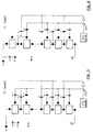
- By referring to the diagram of Fig. 3, the operation of the charge pump stage of the invention is as follows.
- During a first half cycle, when the output of the local oscillator OSC LOC is high (at the regulated voltage VR), the power transistor M1 (high-side driver) is OFF and the power transistor M2 (low-side driver) is ON. Therefore, the output node M of the half-bridge power stage is at ground potential and the bootstrap capacitance Cb charges through the transistor Q2 to the regulated voltage VR present on the node R.
- During the successive half cycle of oscillation, when the output of the oscillator commutes from the voltage VR to ground potential, M2 is switched-OFF and M1 is switched-ON, thus "shortcircuiting" the node R (to which the bootstrap capacitance Cb is connected) to the gate of M1, through the transistor M3. As a consequence, the output node M of the half-bridge stage takes a voltage VR' and the power transistor M1 is kept on during the entire half cycle by the charge stored in the bootstrap capacitance Cb. The voltage VR', assumed by the driving node M, will have the following values:


The transistor Q3 and the Zener DZ2 have the purpose of limiting the voltage on the node M to the value VR', given by the first one of the above-indicated equations. In fact, once the required voltage is reached (i.e. VZ+VBE) , the transistor Q3 switches-OFF the power transistor M1, thus preventing an unnecessary consumption of current through the power transistor M1 itself. - Once the initial switch-ON transient period has terminated, the output charge storing capacitance C2 assumes a potential given by

- As long as the voltage VCP-VCC remains lower than the threshold voltage of the CMOS transistors (M5, M6, M7 and M8), C2 will continue to charge through the diodes intrinsic to the integrated structure of the transistors. As soon as the voltage VCP-VCC becomes greater than the threshold voltage of the CMOS transistors, M5 and M6, driven by the inverting stage constituted by the CMOS pair M7 and M8, will conduct alternatively, cooperating to "pump" electric charge in C2.
- The steady state operation may be described as follows.
- During the half cycle of oscillation when the driving node M is at ground potential, the capacitance C1 charges to VCC through the MOS transistor M5, which is kept ON by the inverting stage formed by the pair of CMOS transistors M7 and M8. In fact, the transistors M5, M6, M7 and M8 are configured in a positive reaction mode (i.e. in a configuration that implements substantially a latch or a flip-flop), and as a consequence, the condition M5on, M6on, persists until the next switching of the driving node M.
- During the following half cycle, when the driving node M assumes the VR' potential, the electric charge that was stored in the transfer capacitance C1 during the preceding half cycle, transfers, thus charging it, into the output storage capacitance C2 through the transistor M6, which is maintained conducting during this half cycle and until a successive switching of the driving node M because of the positive reaction that is implemented through M7-M8.
- From the above considerations, it may be verified easily that the output voltage VCP assumes the following values:


The above formulas are valid for purely capacitive loads. - Of course, when the current absorbed by the load has nonnegligeable value, the internal ON-resistance of transistors M1, M2 and M5 and M6, must be kept in consideration.
- The circuit of the invention has remarkable advantages as compared to the known circuits. The main advantages may be indicated as follows:
- a) reduction of the maximum (multiplied) output voltage by a quantity equivalent to the voltage drop across the transfer diodes of the known circuits can be avoided throughout the range of the supply voltage;
- b) reduction of the maximum output voltage by a quantity equivalent to the voltage drop (Vdrop) through the voltage regulator, under conditions of low supply voltage, may be avoided too;
- c) because the half-bridge, power stage made with the power transistors M1 and M2 is electrically connected to the supply line VCC, the high current peaks that occur for driving the transfer capacitance C1 no longer need to be drawn from the voltage regulator circuit.
- According to an alterantive embodiment of the circuit of the invention, depicted in Fig. 4, the efficiency of the circuit may be increased further.
- As schematically shown in the partial diagram of Fig. 4, the MOS transistors M5 and M6 that functionally replace the diodes D1 and D2 of a conventional circuit, as depicted in Figures 1 and 2, may be separately driven in order to avoid cross-currents and return-currents at switchings. In practice this may implemented by employing two comparators: A1 and A2, or more simply two inverters, one having a low threshold for driving the N-channel transistor M5 and one having a high threshold for driving the P-channel transistor M6.
- In case of integration of the charge pump circuit of the invention, it is recommended to place the transistors M5 and M6 into separate pockets and to bias the pocket of M5 to the bulk potential. Moreover, it is advisable to minimize the gain of the parasitic PNP transistor of the integrated structure of M6, as well as to minimize the parasitic capacitances of the R and S nodes of the circuit depicted in Fig. 3.
- The charge pump circuit of the invention, illustrated above for a voltage "duplicator", may constitute a building block for realizing an N-order voltage multiplier, where N may be theorethically as large as desired.
- A N-even multiplier is depicted in Fig. 5, wherein each three-terminal block (Blk) may be constituted by a circuit as the one composed of transistors M5, M6, M7 and M8 of Fig. 3, or by a circuit similar to the one composed of transistors M5 and M6 and of the respective driving threshold comparators A1 and A2 of Fig. 4.
- An N-odd multiplier is depicted in Fig. 6, wherein each three-terminal block (Blk) may be a circuit as the one composed of transistors M5, M6, M7 and M8 of Fig. 3, or a circuit as the one composed of transistors M5 and M6 and of the respective driving threshold comparators A1 and A2 of Fig. 4.
Claims (8)
- A charge pump circuit comprising
a storage capacitor, functionally connected between an output node on the circuit and a ground node,
two charge transfer devices, functionally connected in series between a supply node and said output node of the circuit,
a charge transfer capacitor, functionally connected between an intermediate node between said two series connected devices and a driving node,
a voltage regulator capable of producing a regulated voltage,
a driving oscillator,
a power stage, controlled by said regulated voltage and driven by said oscillator, whose output node constitutes said driving node to which said charge transfer capacitor is connected,
and characterized by the fact that
each of said charge transfer devices is a switch;
said power stage is a half-bridge stage, functionally connected between said supply node and said ground node and controlled through an inverter which is driven by said oscillator and which is functionally connected between a node at said regulated voltage and said ground node;
a bootstrap capacitor is connected between said driving node at a node at said regulated voltage. - A charge pump circuit as defined in claim 1, wherein said charge transfer switches are constituted by a pair of complementary MOS transistors driven by an inverter formed by a second pair of complementary MOS transistors.
- A charge pump circuit as defined in claim 1, wherein each of said charge transfer switches is independently driven by a driving inverter having a certain triggering threshold.
- A charge pump circuit according to claim 1, wherein said power stage has means capable of limiting the maximum voltage reached by said driving node.
- A charge pump circuit as defined in claim 4, wherein said limiting means are composed of a line comprising a transistor and a Zener diode functionally connected between the output node of said inverter driven by the oscillator and the ground node and said transistor as a control terminal that is functionally connected to said driving node.
- A voltage multiplier comprising a plurality of three-terminal blocks, each having an input, an output and a driving terminal, functionally connected in cascade between a supply node and an output node of the multiplier circuit, the driving terminal of each block being connected to a charge transfer capacitor and the output of each block being connected to a storage capacitor, characterized by the fact that
each block is formed by a pair of switches driven in phase opposition and functionally connected in series between said input and said output of the block, an intermediate node of connect ion between said switches constituting said third driving terminal of the block;
means capable of driving said pair of switches in phase opposition in function of a signal present on said driving node. - A multiplier circuit as defined in claim 6, wherein said means are constituted by an inverter.
- A multiplier circuit as defined in claim 6, wherein said means comprise a pair of threshold comparators.
Priority Applications (4)
| Application Number | Priority Date | Filing Date | Title |
|---|---|---|---|
| DE69310134T DE69310134T2 (en) | 1993-02-17 | 1993-02-17 | Charge pump circuit |
| EP93830059A EP0612140B1 (en) | 1993-02-17 | 1993-02-17 | Charge pump circuit |
| US08/197,077 US5481221A (en) | 1993-02-17 | 1994-02-16 | Charge pump circuit for low supply voltage applications |
| JP4305994A JPH06343260A (en) | 1993-02-17 | 1994-02-17 | Charge pump circuit |
Applications Claiming Priority (1)
| Application Number | Priority Date | Filing Date | Title |
|---|---|---|---|
| EP93830059A EP0612140B1 (en) | 1993-02-17 | 1993-02-17 | Charge pump circuit |
Publications (2)
| Publication Number | Publication Date |
|---|---|
| EP0612140A1 true EP0612140A1 (en) | 1994-08-24 |
| EP0612140B1 EP0612140B1 (en) | 1997-04-23 |
Family
ID=8215120
Family Applications (1)
| Application Number | Title | Priority Date | Filing Date |
|---|---|---|---|
| EP93830059A Expired - Lifetime EP0612140B1 (en) | 1993-02-17 | 1993-02-17 | Charge pump circuit |
Country Status (4)
| Country | Link |
|---|---|
| US (1) | US5481221A (en) |
| EP (1) | EP0612140B1 (en) |
| JP (1) | JPH06343260A (en) |
| DE (1) | DE69310134T2 (en) |
Cited By (3)
| Publication number | Priority date | Publication date | Assignee | Title |
|---|---|---|---|---|
| KR100332646B1 (en) * | 1998-12-23 | 2002-06-20 | 박종섭 | Bootstrap circuit |
| WO2007010018A1 (en) * | 2005-07-21 | 2007-01-25 | Siemens Aktiengesellschaft | Circuit and method for modifying the charge of a capacitive load |
| DE19829806B4 (en) * | 1997-07-03 | 2010-07-08 | DENSO CORPORATION, Kariya-shi | Consumer driver circuit for a vehicle occupant protection device |
Families Citing this family (10)
| Publication number | Priority date | Publication date | Assignee | Title |
|---|---|---|---|---|
| US5767736A (en) * | 1995-11-27 | 1998-06-16 | Lucent Technologies Inc. | Charge pump having high switching speed and low switching noise |
| JPH09288897A (en) * | 1996-04-19 | 1997-11-04 | Sony Corp | Voltage supplying circuit |
| US6448841B1 (en) | 1998-05-01 | 2002-09-10 | Texas Instruments Incorporated | Efficiency charge pump circuit |
| US6344959B1 (en) | 1998-05-01 | 2002-02-05 | Unitrode Corporation | Method for sensing the output voltage of a charge pump circuit without applying a load to the output stage |
| FR2791193B1 (en) * | 1999-03-16 | 2004-07-09 | St Microelectronics Sa | METHOD FOR CONTROLLING THE OPERATION OF A CAPACITIVE CHARGE PUMP AND CORRESPONDING CAPACITIVE CHARGE PUMP DEVICE |
| US6188274B1 (en) | 1999-06-04 | 2001-02-13 | Sharp Laboratories Of America, Inc. | Bootstrap capacitor power supply for low voltage mobile communications power amplifier |
| KR101085698B1 (en) * | 2004-09-08 | 2011-11-22 | 조지아 테크 리서치 코오포레이션 | Apparatus for mixing frequency |
| US20100156513A1 (en) * | 2008-12-23 | 2010-06-24 | Pratt & Whitney Rocketdyne, Inc. | Charge pump |
| US10333397B2 (en) | 2017-07-18 | 2019-06-25 | Stmicroelectronics International N.V. | Multi-stage charge pump circuit operating to simultaneously generate both a positive voltage and a negative voltage |
| US10050524B1 (en) * | 2017-11-01 | 2018-08-14 | Stmicroelectronics International N.V. | Circuit for level shifting a clock signal using a voltage multiplier |
Citations (3)
| Publication number | Priority date | Publication date | Assignee | Title |
|---|---|---|---|---|
| FR2321144A1 (en) * | 1975-08-14 | 1977-03-11 | Ebauches Sa | VOLTAGE MULTIPLIER |
| EP0135889A2 (en) * | 1983-09-29 | 1985-04-03 | Siemens Aktiengesellschaft | Voltage multiplication circuit |
| EP0349495A2 (en) * | 1988-06-28 | 1990-01-03 | STMicroelectronics S.r.l. | CMOS voltage multiplier |
Family Cites Families (7)
| Publication number | Priority date | Publication date | Assignee | Title |
|---|---|---|---|---|
| US3851258A (en) * | 1973-12-13 | 1974-11-26 | Rca Corp | Gateless logic for producing selectable phase clock pulses |
| US4621315A (en) * | 1985-09-03 | 1986-11-04 | Motorola, Inc. | Recirculating MOS charge pump |
| US4669089A (en) * | 1985-09-30 | 1987-05-26 | The Boeing Company | Suppressed clock pulse-duration modulator for direct sequence spread spectrum transmission systems |
| US4809152A (en) * | 1985-10-01 | 1989-02-28 | Maxim Integrated Products | Integrated dual charge pump power supply and RS-232-transmitter/receiver |
| US5051882A (en) * | 1989-01-27 | 1991-09-24 | Teledyne Industries | Three reservoir capacitor charge pump circuit |
| US5038325A (en) * | 1990-03-26 | 1991-08-06 | Micron Technology Inc. | High efficiency charge pump circuit |
| KR930008876B1 (en) * | 1990-08-17 | 1993-09-16 | 현대전자산업 주식회사 | High voltage generating circuit of semicondcutor device |
-
1993
- 1993-02-17 DE DE69310134T patent/DE69310134T2/en not_active Expired - Fee Related
- 1993-02-17 EP EP93830059A patent/EP0612140B1/en not_active Expired - Lifetime
-
1994
- 1994-02-16 US US08/197,077 patent/US5481221A/en not_active Expired - Lifetime
- 1994-02-17 JP JP4305994A patent/JPH06343260A/en active Pending
Patent Citations (3)
| Publication number | Priority date | Publication date | Assignee | Title |
|---|---|---|---|---|
| FR2321144A1 (en) * | 1975-08-14 | 1977-03-11 | Ebauches Sa | VOLTAGE MULTIPLIER |
| EP0135889A2 (en) * | 1983-09-29 | 1985-04-03 | Siemens Aktiengesellschaft | Voltage multiplication circuit |
| EP0349495A2 (en) * | 1988-06-28 | 1990-01-03 | STMicroelectronics S.r.l. | CMOS voltage multiplier |
Non-Patent Citations (1)
| Title |
|---|
| RAMESH PATNAIKUNI, CARR W. N.: "DESIGN AND ANALYSIS OF AN OPTICAL-POWERED ON-CHIP POWER SUPPLY.", PROCEEDINGS OF THE MIDWEST SYMPOSIUM ON CIRCUITS AND SYSTEMS. CHAMPAIGN, AUG. 14 - 16, 1989., NEW YORK, IEEE., US, vol. SYMP. 32, 14 August 1989 (1989-08-14), US, pages 681 - 684., XP000139744 * |
Cited By (4)
| Publication number | Priority date | Publication date | Assignee | Title |
|---|---|---|---|---|
| DE19829806B4 (en) * | 1997-07-03 | 2010-07-08 | DENSO CORPORATION, Kariya-shi | Consumer driver circuit for a vehicle occupant protection device |
| KR100332646B1 (en) * | 1998-12-23 | 2002-06-20 | 박종섭 | Bootstrap circuit |
| WO2007010018A1 (en) * | 2005-07-21 | 2007-01-25 | Siemens Aktiengesellschaft | Circuit and method for modifying the charge of a capacitive load |
| DE102005034164B4 (en) * | 2005-07-21 | 2009-04-30 | Siemens Ag | Circuit and method for changing the charge of a capacitive load |
Also Published As
| Publication number | Publication date |
|---|---|
| DE69310134T2 (en) | 1997-09-18 |
| US5481221A (en) | 1996-01-02 |
| EP0612140B1 (en) | 1997-04-23 |
| DE69310134D1 (en) | 1997-05-28 |
| JPH06343260A (en) | 1994-12-13 |
Similar Documents
| Publication | Publication Date | Title |
|---|---|---|
| US5874850A (en) | Mos voltage elevator of the charge pump type | |
| US6130572A (en) | NMOS negative charge pump | |
| US5717581A (en) | Charge pump circuit with feedback control | |
| US5479333A (en) | Power supply start up booster circuit | |
| US4621315A (en) | Recirculating MOS charge pump | |
| US5689208A (en) | Charge pump circuit for high side switch | |
| EP0685921B1 (en) | Capacitive charge pump, Bicmos circuit for low supply voltage | |
| JP2639325B2 (en) | Constant voltage generator | |
| US4922402A (en) | CMOS voltage multiplier | |
| KR100381971B1 (en) | Self-contained DC-DC converter | |
| EP0612140B1 (en) | Charge pump circuit | |
| US5347171A (en) | Efficient negative charge pump | |
| US5412257A (en) | High efficiency N-channel charge pump having a primary pump and a non-cascaded secondary pump | |
| US6603673B2 (en) | Charge-pump circuit and a load-driving circuit utilizing the same | |
| US7633332B2 (en) | Boosting circuit and boosting method | |
| KR0161308B1 (en) | Power source connecting circuit and switch ic for power supply line | |
| US5914589A (en) | Voltage boosting circuit for high-potential-side MOS switching transistor | |
| US7002399B2 (en) | Basic stage for a charge pump circuit | |
| US7078956B1 (en) | Charge pump circuit | |
| US5381044A (en) | Bootstrap circuit for driving a power MOS transistor | |
| US6483376B1 (en) | Voltage generation circuit of charge pump type, with a self-oscillating control circuit | |
| US5677599A (en) | Circuit for driving an electroluminescent lamp | |
| US5057707A (en) | Charge pump including feedback circuitry for eliminating the requirement of a separate oscillator | |
| US5537072A (en) | Charge pump switch circuits | |
| KR20010113939A (en) | Electronic circuit provided with a digital driver for driving a capacitive load |
Legal Events
| Date | Code | Title | Description |
|---|---|---|---|
| PUAI | Public reference made under article 153(3) epc to a published international application that has entered the european phase |
Free format text: ORIGINAL CODE: 0009012 |
|
| AK | Designated contracting states |
Kind code of ref document: A1 Designated state(s): DE FR GB IT |
|
| 17P | Request for examination filed |
Effective date: 19950121 |
|
| 17Q | First examination report despatched |
Effective date: 19960105 |
|
| GRAG | Despatch of communication of intention to grant |
Free format text: ORIGINAL CODE: EPIDOS AGRA |
|
| GRAH | Despatch of communication of intention to grant a patent |
Free format text: ORIGINAL CODE: EPIDOS IGRA |
|
| GRAH | Despatch of communication of intention to grant a patent |
Free format text: ORIGINAL CODE: EPIDOS IGRA |
|
| GRAA | (expected) grant |
Free format text: ORIGINAL CODE: 0009210 |
|
| AK | Designated contracting states |
Kind code of ref document: B1 Designated state(s): DE FR GB IT |
|
| REF | Corresponds to: |
Ref document number: 69310134 Country of ref document: DE Date of ref document: 19970528 |
|
| ET | Fr: translation filed | ||
| PLBE | No opposition filed within time limit |
Free format text: ORIGINAL CODE: 0009261 |
|
| STAA | Information on the status of an ep patent application or granted ep patent |
Free format text: STATUS: NO OPPOSITION FILED WITHIN TIME LIMIT |
|
| 26N | No opposition filed | ||
| REG | Reference to a national code |
Ref country code: GB Ref legal event code: IF02 |
|
| PGFP | Annual fee paid to national office [announced via postgrant information from national office to epo] |
Ref country code: DE Payment date: 20020306 Year of fee payment: 10 |
|
| PG25 | Lapsed in a contracting state [announced via postgrant information from national office to epo] |
Ref country code: DE Free format text: LAPSE BECAUSE OF NON-PAYMENT OF DUE FEES Effective date: 20030902 |
|
| PGFP | Annual fee paid to national office [announced via postgrant information from national office to epo] |
Ref country code: FR Payment date: 20040210 Year of fee payment: 12 |
|
| PGFP | Annual fee paid to national office [announced via postgrant information from national office to epo] |
Ref country code: GB Payment date: 20040211 Year of fee payment: 12 |
|
| PG25 | Lapsed in a contracting state [announced via postgrant information from national office to epo] |
Ref country code: IT Free format text: LAPSE BECAUSE OF NON-PAYMENT OF DUE FEES;WARNING: LAPSES OF ITALIAN PATENTS WITH EFFECTIVE DATE BEFORE 2007 MAY HAVE OCCURRED AT ANY TIME BEFORE 2007. THE CORRECT EFFECTIVE DATE MAY BE DIFFERENT FROM THE ONE RECORDED. Effective date: 20050217 Ref country code: GB Free format text: LAPSE BECAUSE OF NON-PAYMENT OF DUE FEES Effective date: 20050217 |
|
| GBPC | Gb: european patent ceased through non-payment of renewal fee |
Effective date: 20050217 |
|
| PG25 | Lapsed in a contracting state [announced via postgrant information from national office to epo] |
Ref country code: FR Free format text: LAPSE BECAUSE OF NON-PAYMENT OF DUE FEES Effective date: 20051031 |
|
| REG | Reference to a national code |
Ref country code: FR Ref legal event code: ST Effective date: 20051031 |