EP0611221B1 - Micro-capteur capacitif à faible capacité parasite et procédé de fabrication - Google Patents
Micro-capteur capacitif à faible capacité parasite et procédé de fabrication Download PDFInfo
- Publication number
- EP0611221B1 EP0611221B1 EP94410006A EP94410006A EP0611221B1 EP 0611221 B1 EP0611221 B1 EP 0611221B1 EP 94410006 A EP94410006 A EP 94410006A EP 94410006 A EP94410006 A EP 94410006A EP 0611221 B1 EP0611221 B1 EP 0611221B1
- Authority
- EP
- European Patent Office
- Prior art keywords
- stripe
- silicon
- plates
- isolating
- external
- Prior art date
- Legal status (The legal status is an assumption and is not a legal conclusion. Google has not performed a legal analysis and makes no representation as to the accuracy of the status listed.)
- Expired - Lifetime
Links
- 238000004519 manufacturing process Methods 0.000 title claims description 15
- 230000003071 parasitic effect Effects 0.000 title description 7
- XUIMIQQOPSSXEZ-UHFFFAOYSA-N Silicon Chemical compound [Si] XUIMIQQOPSSXEZ-UHFFFAOYSA-N 0.000 claims description 35
- 229910052710 silicon Inorganic materials 0.000 claims description 34
- 239000010703 silicon Substances 0.000 claims description 34
- VYPSYNLAJGMNEJ-UHFFFAOYSA-N Silicium dioxide Chemical compound O=[Si]=O VYPSYNLAJGMNEJ-UHFFFAOYSA-N 0.000 claims description 9
- 229910052814 silicon oxide Inorganic materials 0.000 claims description 9
- 238000005530 etching Methods 0.000 claims description 6
- 230000003647 oxidation Effects 0.000 claims description 6
- 238000007254 oxidation reaction Methods 0.000 claims description 6
- 238000005520 cutting process Methods 0.000 claims description 4
- 230000002093 peripheral effect Effects 0.000 claims description 2
- 230000001590 oxidative effect Effects 0.000 claims 1
- 235000012431 wafers Nutrition 0.000 description 23
- 238000000034 method Methods 0.000 description 9
- 230000001133 acceleration Effects 0.000 description 6
- 239000011521 glass Substances 0.000 description 5
- 229910052581 Si3N4 Inorganic materials 0.000 description 4
- HQVNEWCFYHHQES-UHFFFAOYSA-N silicon nitride Chemical compound N12[Si]34N5[Si]62N3[Si]51N64 HQVNEWCFYHHQES-UHFFFAOYSA-N 0.000 description 4
- 238000009413 insulation Methods 0.000 description 3
- 239000012212 insulator Substances 0.000 description 3
- 239000012528 membrane Substances 0.000 description 3
- 238000000926 separation method Methods 0.000 description 3
- 241000446313 Lamella Species 0.000 description 2
- 238000002955 isolation Methods 0.000 description 2
- 238000005259 measurement Methods 0.000 description 2
- 229910021420 polycrystalline silicon Inorganic materials 0.000 description 2
- 239000004065 semiconductor Substances 0.000 description 2
- 239000000725 suspension Substances 0.000 description 2
- 238000000137 annealing Methods 0.000 description 1
- 238000009412 basement excavation Methods 0.000 description 1
- 230000000295 complement effect Effects 0.000 description 1
- 230000008094 contradictory effect Effects 0.000 description 1
- 238000004320 controlled atmosphere Methods 0.000 description 1
- 230000008021 deposition Effects 0.000 description 1
- 238000010438 heat treatment Methods 0.000 description 1
- 230000000873 masking effect Effects 0.000 description 1
- 238000012986 modification Methods 0.000 description 1
- 230000004048 modification Effects 0.000 description 1
- 150000004767 nitrides Chemical class 0.000 description 1
- 230000035515 penetration Effects 0.000 description 1
- XUIMIQQOPSSXEZ-AKLPVKDBSA-N silicon-31 atom Chemical compound [31Si] XUIMIQQOPSSXEZ-AKLPVKDBSA-N 0.000 description 1
Images


Classifications
-
- G—PHYSICS
- G01—MEASURING; TESTING
- G01P—MEASURING LINEAR OR ANGULAR SPEED, ACCELERATION, DECELERATION, OR SHOCK; INDICATING PRESENCE, ABSENCE, OR DIRECTION, OF MOVEMENT
- G01P15/00—Measuring acceleration; Measuring deceleration; Measuring shock, i.e. sudden change of acceleration
- G01P15/02—Measuring acceleration; Measuring deceleration; Measuring shock, i.e. sudden change of acceleration by making use of inertia forces using solid seismic masses
- G01P15/08—Measuring acceleration; Measuring deceleration; Measuring shock, i.e. sudden change of acceleration by making use of inertia forces using solid seismic masses with conversion into electric or magnetic values
- G01P15/125—Measuring acceleration; Measuring deceleration; Measuring shock, i.e. sudden change of acceleration by making use of inertia forces using solid seismic masses with conversion into electric or magnetic values by capacitive pick-up
-
- G—PHYSICS
- G01—MEASURING; TESTING
- G01D—MEASURING NOT SPECIALLY ADAPTED FOR A SPECIFIC VARIABLE; ARRANGEMENTS FOR MEASURING TWO OR MORE VARIABLES NOT COVERED IN A SINGLE OTHER SUBCLASS; TARIFF METERING APPARATUS; MEASURING OR TESTING NOT OTHERWISE PROVIDED FOR
- G01D5/00—Mechanical means for transferring the output of a sensing member; Means for converting the output of a sensing member to another variable where the form or nature of the sensing member does not constrain the means for converting; Transducers not specially adapted for a specific variable
- G01D5/12—Mechanical means for transferring the output of a sensing member; Means for converting the output of a sensing member to another variable where the form or nature of the sensing member does not constrain the means for converting; Transducers not specially adapted for a specific variable using electric or magnetic means
- G01D5/14—Mechanical means for transferring the output of a sensing member; Means for converting the output of a sensing member to another variable where the form or nature of the sensing member does not constrain the means for converting; Transducers not specially adapted for a specific variable using electric or magnetic means influencing the magnitude of a current or voltage
- G01D5/24—Mechanical means for transferring the output of a sensing member; Means for converting the output of a sensing member to another variable where the form or nature of the sensing member does not constrain the means for converting; Transducers not specially adapted for a specific variable using electric or magnetic means influencing the magnitude of a current or voltage by varying capacitance
- G01D5/241—Mechanical means for transferring the output of a sensing member; Means for converting the output of a sensing member to another variable where the form or nature of the sensing member does not constrain the means for converting; Transducers not specially adapted for a specific variable using electric or magnetic means influencing the magnitude of a current or voltage by varying capacitance by relative movement of capacitor electrodes
- G01D5/2417—Mechanical means for transferring the output of a sensing member; Means for converting the output of a sensing member to another variable where the form or nature of the sensing member does not constrain the means for converting; Transducers not specially adapted for a specific variable using electric or magnetic means influencing the magnitude of a current or voltage by varying capacitance by relative movement of capacitor electrodes by varying separation
-
- G—PHYSICS
- G01—MEASURING; TESTING
- G01L—MEASURING FORCE, STRESS, TORQUE, WORK, MECHANICAL POWER, MECHANICAL EFFICIENCY, OR FLUID PRESSURE
- G01L9/00—Measuring steady of quasi-steady pressure of fluid or fluent solid material by electric or magnetic pressure-sensitive elements; Transmitting or indicating the displacement of mechanical pressure-sensitive elements, used to measure the steady or quasi-steady pressure of a fluid or fluent solid material, by electric or magnetic means
- G01L9/0041—Transmitting or indicating the displacement of flexible diaphragms
- G01L9/0072—Transmitting or indicating the displacement of flexible diaphragms using variations in capacitance
- G01L9/0073—Transmitting or indicating the displacement of flexible diaphragms using variations in capacitance using a semiconductive diaphragm
-
- G—PHYSICS
- G01—MEASURING; TESTING
- G01P—MEASURING LINEAR OR ANGULAR SPEED, ACCELERATION, DECELERATION, OR SHOCK; INDICATING PRESENCE, ABSENCE, OR DIRECTION, OF MOVEMENT
- G01P15/00—Measuring acceleration; Measuring deceleration; Measuring shock, i.e. sudden change of acceleration
- G01P15/02—Measuring acceleration; Measuring deceleration; Measuring shock, i.e. sudden change of acceleration by making use of inertia forces using solid seismic masses
- G01P15/08—Measuring acceleration; Measuring deceleration; Measuring shock, i.e. sudden change of acceleration by making use of inertia forces using solid seismic masses with conversion into electric or magnetic values
- G01P2015/0805—Measuring acceleration; Measuring deceleration; Measuring shock, i.e. sudden change of acceleration by making use of inertia forces using solid seismic masses with conversion into electric or magnetic values being provided with a particular type of spring-mass-system for defining the displacement of a seismic mass due to an external acceleration
- G01P2015/0822—Measuring acceleration; Measuring deceleration; Measuring shock, i.e. sudden change of acceleration by making use of inertia forces using solid seismic masses with conversion into electric or magnetic values being provided with a particular type of spring-mass-system for defining the displacement of a seismic mass due to an external acceleration for defining out-of-plane movement of the mass
- G01P2015/0825—Measuring acceleration; Measuring deceleration; Measuring shock, i.e. sudden change of acceleration by making use of inertia forces using solid seismic masses with conversion into electric or magnetic values being provided with a particular type of spring-mass-system for defining the displacement of a seismic mass due to an external acceleration for defining out-of-plane movement of the mass for one single degree of freedom of movement of the mass
- G01P2015/0828—Measuring acceleration; Measuring deceleration; Measuring shock, i.e. sudden change of acceleration by making use of inertia forces using solid seismic masses with conversion into electric or magnetic values being provided with a particular type of spring-mass-system for defining the displacement of a seismic mass due to an external acceleration for defining out-of-plane movement of the mass for one single degree of freedom of movement of the mass the mass being of the paddle type being suspended at one of its longitudinal ends
Definitions
- the present invention relates to the field of micro-sensors capacitive silicon.
- micro-sensors can for example building up pressure sensors, sensors acceleration ...
- micro-sensors taking advantage of techniques of silicon engraving developed as part of the manufacture of semiconductor electronic components.
- micro-sensors consisted of the assembly suitably engraved silicon wafers and blades thin glass used as a waterproof case or plates of insulating separation between silicon wafers, these blades of glass possibly carrying various patterns of electrodes metallic.
- the sensor of Figure 1 is an acceleration sensor and the sensor of FIG. 2 a pressure sensor.
- Each of these sensors includes a central silicon wafer 1 sandwiched between external silicon wafers 2 and 3.
- the isolation between the plates is ensured by a first insulating strip 5, generally a layer of silicon oxide, between plates 1 and 2 and a second insulating strip 6 between plates 1 and 3.
- These insulating strips take the form of a frame arranged between adjacent plates, the along the edges of these. Oxide bands can be obtained by growth or deposit from one of the platelets adjacent then engraving.
- silicon surfaces and of silicon oxide facing have very low roughness, for example less than 0.5 nm.
- Silicon wafers extremes 2 and 3 define between them and with the part of frame of the silicon wafer 1 a region in which is contained a controlled atmosphere, for example a very low pressure, called vacuum.
- FIG. 1 schematically represents a sectional view of an accelerometer
- the plate of central silicon 1 is etched before assembly to understand a frame and a central plate or counterweight 8 fixed to the frame by thin bars of suspension 9.
- a single bar appears in the schematic sectional view of FIG. 1.
- the external plates 2 and 3 delimit with the frame formed at the periphery of the central plate an empty space.
- the counterweight 8 moves relative to the entire device and capabilities listed above vary. he is also generally provided an electrostatic servo for hold the flyweight in place by applying a field continuous electrical and the error signal then gives an indication of the change in capacity.
- Figure 2 very schematically represents a structure constituting a pressure sensor.
- the lower plate 2 is etched to form a thin membrane 11.
- the plate 1 is etched to form a stud 12 supported on this membrane.
- a silicon wafer 13 extends between this stud and the frame of the plate 1. Again, the space delimited by the upper plate, the lower plate and the central plate frame defines an empty space. Variations in external pressure deform the membrane 11 and cause the lamella tension to vary 13.
- This variation in voltage causes a variation in the resonant frequency of the capacitive resonator constituted by the strip 13 and the facing surface of the wafer 3.
- the internal face of the plate 3 is etched to form a protruding strip opposite the lamella 13.
- electrodes 21, 22 and 23 must be respectively attached to plates 1, 2 and 3. In the case of FIG. 2, only the electrodes 21 and 23 will be required.
- the thickness of the frame 1 is in a simple manufacturing process the same as the thickness of the counterweight 8.
- the thickness of the layers insulators (oxide) 5 and 6 defines, on the one hand, the value of the interval between the counterweight and each of the opposite faces, on the other hand, the isolation between silicon wafers. This thickness must be small so that the active capacity (defined by the interval between the counterweight and the facing faces) be as large as possible. In contrast, this thickness should be as large as possible to limit the parasitic capacity.
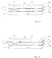
- the aforementioned patent application proposes (as illustrated in its figure 4 shown in Figure 3 attached) to deposit layers of polycrystalline silicon 16, 18 on the internal faces of external pads, opposite the counterweight, to reduce the interval between the counterweight and the facing faces.
- this process is relatively complex since requires additional manufacturing steps including a deposition of polycrystalline silicon and an etching thereof on the internal faces.
- Another solution is proposed in this earlier patent application in relation to its figure figure 24. It consists on the one hand of making the thickness unequal of the counterweight and the thickness of the frame, on the other hand to dig the external faces and fill them with an insulating glass at the contact points. Again, this is a process complex and the use of glass deposits is not without disadvantages.
- an object of the present invention is to provide a new capacitive micro-sensor structure in which parasitic capacities are reduced.
- Another object of the present invention is to provide such a structure in which variations of these are avoided capacities from one component to another and over time.
- the present invention provides a capacitive micro-sensor including a sandwich of three silicon wafers, peripheral band of the face internal of each external plate being attached to a strip corresponding from the opposite face of the central plate by through an insulating strip.
- the insulating tape is a silicon oxide strip which partially penetrates inside external platelets.
- the projecting height of the insulating strip is substantially the half of its total thickness.
- the present invention also provides a method of manufacture of the aforementioned capacitive micro-sensor which consists to assemble three separate silicon wafers together, at least at their periphery, by an insulating strip, each of these plates initially forming part of a silicon wafer, individual devices being formed by cutting the assembly of slices, in which the strip insulator is formed by localized oxidation of platelets external.
- the present invention also provides a method of manufacture of the aforementioned capacitive micro-sensor which consists to assemble three separate silicon wafers together, at least at their periphery, by an insulating strip, each of these plates initially forming part of a silicon wafer, individual devices being formed by cutting the assembly of slices, in which the strip insulator is formed by digging appropriate regions of external platelets, oxidation and etching of the oxide outside hollowed out regions.
- the thicknesses do not are not drawn to scale and are arbitrarily expanded to make the figures readable.
- the thicknesses silicon wafers are in the range of 300 to 500 micrometers while the thicknesses of the insulation layers are in the range of 2 to 4 micrometers.
- the lateral dimensions of each component may be of the order of 3 to 6 mm.
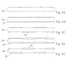
- Figure 4 shows a sectional view of a device according to the present invention.
- the insulation layers for separating the outer pads from the center pad are oxide layers which partially penetrate and partially protrude from the outer pads.
- their protruding thickness d1 delimits the interval between the counterweight and the external plates while their total thickness d2 determines the value of the parasitic capacities. It is therefore possible to limit the value of the stray capacitances without reducing the value of the active interval.
- Such a structure can be manufactured simply by various conventional processes using oxide layers silicon.
- FIGS. 5A to 5E represent successive stages manufacturing using the conventional process designated in the semiconductor technique under the name "LOCOS". These FIGS. 5A to 5E represent an external silicon wafer.
- FIG. 5A represents a bare section 30.
- this layer of silicon nitride has a thickness of a hundred nanometers and is deposited on a very thin layer of silicon oxide with a thickness of one ten nanometers.
- the nitride layer of silicon 31 is etched to leave regions 32 in place.
- thermal oxidation is realized which only occurs in the openings made between regions 32. This gives oxide regions 33 which penetrate from a certain depth into the silicon wafer and protrude from a determined height.
- the engraving of silicon nitride can be followed by etching of the oxide of silicon to project only a selected height silicon oxide.
- the projecting height is substantially equal to the depth of penetration. So if the silicon oxide layer has a total thickness of the order of 2 micrometers, the projecting height will be around 1 micrometer or less. We can consider growing layers oxide having total thicknesses of up to 3 to 4 micrometers.
- FIG. 6 it is then possible to assemble two external sections such as section 30, respectively designated by the references 30 and 40 on either side of a central section 35, section 40 comprising oxide regions 43 symmetrical of the oxide regions 33.
- the central section has a conventional structure known in the art.
- the assembly is then welded by heat treatment and the desired result is obtained, namely that the thickness d2 of the oxide 33 contributing to the definition of the parasitic capacitances is greater than the interval d1 between the counterweight and the external sections.
- the assembly of the three slices can conventionally be divided into elementary components such as that of FIG. 4 by sawing along the lines indicated in dotted lines by the references 50.
- FIG. 7 represents another mode of separation into elementary components.
- regions 34 and 44 previously defined as mask of etching the external silicon wafers 30 and 40. And we etch these platelets until reaching the oxide layers 33 and 43. It is only after this engraving of the external plates that we separate into elementary components by sawing along lines 50.
- this second embodiment of the invention we have the advantage of increasing the thickness of the insulation between platelets but we have an additional advantage linked to the fact that sawing is not carried out along the edge of the device and is therefore not likely to cause chips silicon at the visible walls of the oxide bands side.
- the present invention is capable of many variants which will appear to those skilled in the art.
- the "LOCOS" process instead of using the "LOCOS" process to train partially buried oxide regions 33 we could first etch the external silicon wafers, leaving excavations at the level of regions 33, then proceed to uniform oxidation and remove the silicon oxide by masking outside the hollow zones. We then obtain substantially the same result.
- the present invention is susceptible of numerous variants and modifications which will appear to those skilled in the art.
- an embodiment of the invention has been described in relationship with a very schematic accelerometer.
- Many other accelerometer structures are known in the art and it will again be emphasized that the present invention applies also to structures of the pressure sensor type such than that illustrated in figure 2.
Landscapes
- Physics & Mathematics (AREA)
- General Physics & Mathematics (AREA)
- Engineering & Computer Science (AREA)
- Power Engineering (AREA)
- Pressure Sensors (AREA)
- Measuring Fluid Pressure (AREA)
Description
Claims (4)
- Micro-capteur capacitif comprenant un sandwich de trois plaquettes de silicium (1, 2, 3), une bande périphérique de la face interne de chaque plaquette externe étant accolée à une bande correspondante de la face en regard de la plaquette centrale par l'intermédiaire d'une bande isolante (5, 6), caractérisé en ce que ladite bande isolante est une bande d'oxyde de silicium qui pénètre partiellement à l'intérieur des plaquettes externes (2, 3).
- Micro-capteur capacitif selon la revendication 1, caractérisé en ce que la hauteur en saillie (d1) de la bande isolante (5, 6) est sensiblement la moitié de son épaisseur totale (d2).
- Procédé de fabrication d'un micro-capteur capacitif selon la revendication 1, consistant à assembler trois plaquettes de silicium séparées entre elles, au moins au niveau de leur pourtour, par une bande isolante (33, 43), chacune de ces plaquettes faisant initialement partie d'une tranche de silicium (30, 35, 40), des dispositifs individuels étant formés par découpe de l'assemblage de tranches, caractérisé en ce que ladite bande isolante (33, 43) est formée par oxydation localisée des plaquettes externes (30, 40).
- Procédé de fabrication d'un micro-capteur capacitif selon la revendication 1, consistant à assembler trois plaquettes de silicium séparées entre elles, au moins au niveau de leur pourtour, par une bande isolante (33, 43), chacune de ces plaquettes faisant initialement partie d'une tranche de silicium (30, 35, 40), des dispositifs individuels étant formés par découpe de l'assemblage de tranches, caractérisé en ce que ladite bande isolante (33, 43) est formée par creusement des régions appropriées des plaquettes externes (30, 40), oxydation et gravure de l'oxyde en dehors des régions creusées.
Applications Claiming Priority (2)
| Application Number | Priority Date | Filing Date | Title |
|---|---|---|---|
| FR9301742A FR2701562B1 (fr) | 1993-02-10 | 1993-02-10 | Micro-capteur capacitif à faible capcité parasite et procédé de fabrication. |
| FR9301742 | 1993-02-10 |
Publications (2)
| Publication Number | Publication Date |
|---|---|
| EP0611221A1 EP0611221A1 (fr) | 1994-08-17 |
| EP0611221B1 true EP0611221B1 (fr) | 1998-05-06 |
Family
ID=9444115
Family Applications (1)
| Application Number | Title | Priority Date | Filing Date |
|---|---|---|---|
| EP94410006A Expired - Lifetime EP0611221B1 (fr) | 1993-02-10 | 1994-02-08 | Micro-capteur capacitif à faible capacité parasite et procédé de fabrication |
Country Status (3)
| Country | Link |
|---|---|
| EP (1) | EP0611221B1 (fr) |
| DE (1) | DE69409991T2 (fr) |
| FR (1) | FR2701562B1 (fr) |
Families Citing this family (5)
| Publication number | Priority date | Publication date | Assignee | Title |
|---|---|---|---|---|
| DE4439238A1 (de) * | 1994-11-03 | 1996-05-09 | Telefunken Microelectron | Kapazitiver Beschleunigungssensor |
| GB9524624D0 (en) * | 1995-12-01 | 1996-01-31 | Weston Aerospace Ltd | Pressure sensor |
| WO2006127814A2 (fr) | 2005-05-25 | 2006-11-30 | Northrop Grumman Corporation | Optimisation de la largeur de ligne de liaison directe a la micro-plaquette pour reduire la capacitance parasite dans les accelerometres en technologie des systemes micro-electromecaniques |
| WO2006127813A2 (fr) * | 2005-05-25 | 2006-11-30 | Northrop Grumman Corporation | Amelioration du rapport signal/bruit dans des microcircuits accelerometres en technologie des systemes micro-electromecaniques sur substrat et autres dispositifs en technologie des systemes micro-electromecaniques |
| CN119470972B (zh) * | 2024-11-14 | 2025-11-14 | 华中科技大学 | 一种低寄生电容的mems加速度计及制备方法 |
Family Cites Families (3)
| Publication number | Priority date | Publication date | Assignee | Title |
|---|---|---|---|---|
| JPS5516228A (en) * | 1978-07-21 | 1980-02-04 | Hitachi Ltd | Capacity type sensor |
| JPH0623782B2 (ja) * | 1988-11-15 | 1994-03-30 | 株式会社日立製作所 | 静電容量式加速度センサ及び半導体圧力センサ |
| US4879627A (en) * | 1988-12-30 | 1989-11-07 | United Technologies Corporation | Differential capacitive pressure sensor with over-pressure protection |
-
1993
- 1993-02-10 FR FR9301742A patent/FR2701562B1/fr not_active Expired - Fee Related
-
1994
- 1994-02-08 DE DE69409991T patent/DE69409991T2/de not_active Expired - Fee Related
- 1994-02-08 EP EP94410006A patent/EP0611221B1/fr not_active Expired - Lifetime
Also Published As
| Publication number | Publication date |
|---|---|
| DE69409991T2 (de) | 1998-12-24 |
| FR2701562B1 (fr) | 1995-05-05 |
| EP0611221A1 (fr) | 1994-08-17 |
| FR2701562A1 (fr) | 1994-08-19 |
| DE69409991D1 (de) | 1998-06-10 |
Similar Documents
| Publication | Publication Date | Title |
|---|---|---|
| EP0557217B1 (fr) | Micro-capteur capacitif à faible capacité parasite et procédé de fabrication | |
| EP0557219B1 (fr) | Micro-capteur capacitif à capacité parasite réduite et procédé de fabrication | |
| EP0605302B1 (fr) | Procédé de fabrication d'un capteur de pression utilisant la technologie silicium sur isolant et capteur obtenu | |
| EP1248366B1 (fr) | Résonateur électromécanique à poutre vibrante | |
| US6973835B2 (en) | Pressure sensor | |
| EP0754953B1 (fr) | Procédé de fabrication d'une structure avec une couche utile maintenue à distance d'un substrat par des butées, et de désolidarisation d'une telle couche | |
| EP0596456A1 (fr) | Procédé de fabrication de transducteurs capacitifs intégrés | |
| FR2736205A1 (fr) | Dispositif detecteur a semiconducteur et son procede de formation | |
| EP1027583A1 (fr) | Structure munie de contacts electriques formes a travers le substrat de cette structure et procede d'obtention d'une telle structure | |
| EP0983609B1 (fr) | Procede de fabrication d'un micro-capteur en silicium usine | |
| EP0610806A1 (fr) | Capteur de mesure de pression absolue de type capacitif et procédé de fabrication d'une pluralité de tels capteurs | |
| EP0557216B1 (fr) | Micro-capteur de pression | |
| FR2897937A1 (fr) | Capteur de pression a jauges resistives | |
| EP0611221A1 (fr) | Micro-capteur capacitif à faible capacité parasite et procédé de fabrication | |
| EP0783676B1 (fr) | Micro-capteur capacitif a faible capacite parasite | |
| EP0684479B1 (fr) | Microaccéléromètre à résonateur compensé en température | |
| EP0864094B1 (fr) | Structure comprenant une partie isolee dans un substrat massif et procede de realisation d'une telle structure | |
| FR2738705A1 (fr) | Dispositif capteur electromecanique et procede de fabrication d'un tel dispositif | |
| EP0611222B1 (fr) | Procédé de découpe d'un microcapteur capacitif | |
| EP0557220B1 (fr) | Micro-capteur capacitif à protection latérale et procédé de fabrication | |
| EP0362090A1 (fr) | Procédé de fabrication d'une pièce mécanique comportant un élément sensible d'épaisseur donnée et pièce mécanique obtenue | |
| WO2002076881A1 (fr) | Procede de fabrication d'une structure a membrane micro-usinee | |
| EP0613011A1 (fr) | Montage de micro-capteur | |
| FR3074358A1 (fr) | Procede de realisation d'une cavite etanche a couche mince |
Legal Events
| Date | Code | Title | Description |
|---|---|---|---|
| PUAI | Public reference made under article 153(3) epc to a published international application that has entered the european phase |
Free format text: ORIGINAL CODE: 0009012 |
|
| AK | Designated contracting states |
Kind code of ref document: A1 Designated state(s): CH DE FR GB IT LI |
|
| 17P | Request for examination filed |
Effective date: 19950124 |
|
| 17Q | First examination report despatched |
Effective date: 19960925 |
|
| GRAG | Despatch of communication of intention to grant |
Free format text: ORIGINAL CODE: EPIDOS AGRA |
|
| GRAG | Despatch of communication of intention to grant |
Free format text: ORIGINAL CODE: EPIDOS AGRA |
|
| GRAH | Despatch of communication of intention to grant a patent |
Free format text: ORIGINAL CODE: EPIDOS IGRA |
|
| GRAH | Despatch of communication of intention to grant a patent |
Free format text: ORIGINAL CODE: EPIDOS IGRA |
|
| GRAA | (expected) grant |
Free format text: ORIGINAL CODE: 0009210 |
|
| AK | Designated contracting states |
Kind code of ref document: B1 Designated state(s): CH DE FR GB IT LI |
|
| REG | Reference to a national code |
Ref country code: CH Ref legal event code: EP |
|
| REF | Corresponds to: |
Ref document number: 69409991 Country of ref document: DE Date of ref document: 19980610 |
|
| ITF | It: translation for a ep patent filed | ||
| GBT | Gb: translation of ep patent filed (gb section 77(6)(a)/1977) |
Effective date: 19980722 |
|
| REG | Reference to a national code |
Ref country code: CH Ref legal event code: NV Representative=s name: MOINAS SAVOYE & CRONIN |
|
| PLBE | No opposition filed within time limit |
Free format text: ORIGINAL CODE: 0009261 |
|
| STAA | Information on the status of an ep patent application or granted ep patent |
Free format text: STATUS: NO OPPOSITION FILED WITHIN TIME LIMIT |
|
| 26N | No opposition filed | ||
| REG | Reference to a national code |
Ref country code: GB Ref legal event code: IF02 |
|
| PGFP | Annual fee paid to national office [announced via postgrant information from national office to epo] |
Ref country code: GB Payment date: 20050202 Year of fee payment: 12 |
|
| PGFP | Annual fee paid to national office [announced via postgrant information from national office to epo] |
Ref country code: DE Payment date: 20050203 Year of fee payment: 12 |
|
| PG25 | Lapsed in a contracting state [announced via postgrant information from national office to epo] |
Ref country code: IT Free format text: LAPSE BECAUSE OF NON-PAYMENT OF DUE FEES;WARNING: LAPSES OF ITALIAN PATENTS WITH EFFECTIVE DATE BEFORE 2007 MAY HAVE OCCURRED AT ANY TIME BEFORE 2007. THE CORRECT EFFECTIVE DATE MAY BE DIFFERENT FROM THE ONE RECORDED. Effective date: 20050208 |
|
| PGFP | Annual fee paid to national office [announced via postgrant information from national office to epo] |
Ref country code: FR Payment date: 20050208 Year of fee payment: 12 |
|
| PGFP | Annual fee paid to national office [announced via postgrant information from national office to epo] |
Ref country code: CH Payment date: 20050216 Year of fee payment: 12 |
|
| PG25 | Lapsed in a contracting state [announced via postgrant information from national office to epo] |
Ref country code: GB Free format text: LAPSE BECAUSE OF NON-PAYMENT OF DUE FEES Effective date: 20060208 |
|
| PG25 | Lapsed in a contracting state [announced via postgrant information from national office to epo] |
Ref country code: LI Free format text: LAPSE BECAUSE OF NON-PAYMENT OF DUE FEES Effective date: 20060228 Ref country code: CH Free format text: LAPSE BECAUSE OF NON-PAYMENT OF DUE FEES Effective date: 20060228 |
|
| PG25 | Lapsed in a contracting state [announced via postgrant information from national office to epo] |
Ref country code: DE Free format text: LAPSE BECAUSE OF NON-PAYMENT OF DUE FEES Effective date: 20060901 |
|
| REG | Reference to a national code |
Ref country code: CH Ref legal event code: PL |
|
| GBPC | Gb: european patent ceased through non-payment of renewal fee |
Effective date: 20060208 |
|
| REG | Reference to a national code |
Ref country code: FR Ref legal event code: ST Effective date: 20061031 |
|
| PG25 | Lapsed in a contracting state [announced via postgrant information from national office to epo] |
Ref country code: FR Free format text: LAPSE BECAUSE OF NON-PAYMENT OF DUE FEES Effective date: 20060228 |