EP0608209A2 - Dispositif photo-électrique pour mesurer la position - Google Patents
Dispositif photo-électrique pour mesurer la position Download PDFInfo
- Publication number
- EP0608209A2 EP0608209A2 EP94890010A EP94890010A EP0608209A2 EP 0608209 A2 EP0608209 A2 EP 0608209A2 EP 94890010 A EP94890010 A EP 94890010A EP 94890010 A EP94890010 A EP 94890010A EP 0608209 A2 EP0608209 A2 EP 0608209A2
- Authority
- EP
- European Patent Office
- Prior art keywords
- phase grating
- scale
- diffraction
- scanning
- grating
- Prior art date
- Legal status (The legal status is an assumption and is not a legal conclusion. Google has not performed a legal analysis and makes no representation as to the accuracy of the status listed.)
- Granted
Links
- 230000003287 optical effect Effects 0.000 claims abstract description 10
- 238000005259 measurement Methods 0.000 claims abstract description 6
- 230000000737 periodic effect Effects 0.000 claims abstract description 3
- 238000005070 sampling Methods 0.000 claims description 4
- 238000009434 installation Methods 0.000 abstract 1
- 241000669003 Aspidiotus destructor Species 0.000 description 2
- 238000010276 construction Methods 0.000 description 1
- 230000001419 dependent effect Effects 0.000 description 1
- 238000013461 design Methods 0.000 description 1
- 238000011161 development Methods 0.000 description 1
- 238000010586 diagram Methods 0.000 description 1
- 230000000694 effects Effects 0.000 description 1
- 230000008030 elimination Effects 0.000 description 1
- 238000003379 elimination reaction Methods 0.000 description 1
- 238000011156 evaluation Methods 0.000 description 1
- 238000004519 manufacturing process Methods 0.000 description 1
- 238000012544 monitoring process Methods 0.000 description 1
- 230000007935 neutral effect Effects 0.000 description 1
- 238000000926 separation method Methods 0.000 description 1
Images
Classifications
-
- G—PHYSICS
- G01—MEASURING; TESTING
- G01D—MEASURING NOT SPECIALLY ADAPTED FOR A SPECIFIC VARIABLE; ARRANGEMENTS FOR MEASURING TWO OR MORE VARIABLES NOT COVERED IN A SINGLE OTHER SUBCLASS; TARIFF METERING APPARATUS; MEASURING OR TESTING NOT OTHERWISE PROVIDED FOR
- G01D5/00—Mechanical means for transferring the output of a sensing member; Means for converting the output of a sensing member to another variable where the form or nature of the sensing member does not constrain the means for converting; Transducers not specially adapted for a specific variable
- G01D5/26—Mechanical means for transferring the output of a sensing member; Means for converting the output of a sensing member to another variable where the form or nature of the sensing member does not constrain the means for converting; Transducers not specially adapted for a specific variable characterised by optical transfer means, i.e. using infrared, visible, or ultraviolet light
- G01D5/32—Mechanical means for transferring the output of a sensing member; Means for converting the output of a sensing member to another variable where the form or nature of the sensing member does not constrain the means for converting; Transducers not specially adapted for a specific variable characterised by optical transfer means, i.e. using infrared, visible, or ultraviolet light with attenuation or whole or partial obturation of beams of light
- G01D5/34—Mechanical means for transferring the output of a sensing member; Means for converting the output of a sensing member to another variable where the form or nature of the sensing member does not constrain the means for converting; Transducers not specially adapted for a specific variable characterised by optical transfer means, i.e. using infrared, visible, or ultraviolet light with attenuation or whole or partial obturation of beams of light the beams of light being detected by photocells
- G01D5/36—Forming the light into pulses
- G01D5/38—Forming the light into pulses by diffraction gratings
Definitions
- the invention relates to a photoelectric position measuring device, with a scale phase grating, at least one scanning phase grating which can be adjusted relative to the scale, at least one light source with a collimator and photo receivers which is fixed relative to the scanning phase grating (s), the groups of the diffraction order determined by the two Diffraction of the light on the phase grating (s) and the at least one-time diffraction on the scale phase grating receive interference images and correspondingly generate periodic, mutually phase-shifted measurement signals from their changes in intensity during the relative adjustment of scanning and scale phase grids.
- Such a position measuring device is known, inter alia, from EP-A-0 509 979.
- Such position measuring devices work according to the principle of the so-called three-grating step encoder, the bases of which are explained in detail in theory in the dissertation by J. Wilhelm published in 1978 "Three-grating stepper photoelectric transducer for measuring changes in position" (TU Hannover). With reflective phase gratings as a scale, the light in the sampling phase grating is diffracted twice.
- a further scanning phase grating can be provided on the second scale side and finally it is also possible for the light diffracted by the first scanning phase grating and the transparent scale to be passed via a diverting prism on the back of the scale over a section of the scale length and then through the scale and to lead another scanning grating to the receivers so that there is a double diffraction of the light on the scale.
- phase errors can occur with all three-grating step encoders of the previous type, in particular due to pitch errors of the individual gratings and / or mounting tolerances of the scanning grids with respect to the scale grating (s) and due to tilting of the scanning grids, so that lengthy adjustment settings are necessary to achieve usable signals during the measurement.
- the object of the invention is to provide a measuring device of the type mentioned at the outset, in which large mounting tolerances are permissible with simple manufacture and simple adjustment for the adjustment of the phase error is made possible.
- the object is achieved in that at least one optical guide device which fuses the light beam subjected to diffraction across the diffraction direction on scale and scanning phase gratings in two partial beam regions is switched on in the light beam path and separate photo receivers are provided for the groups with the same diffraction direction of the partial beam light beams.
- the position measuring device enables the use of simple scale and scanning gratings, the desired phase-shifted signal pairs being nevertheless generated and the possibility of also generating the phase-shifted signal pairs from immediately adjacent or merging scanning points of the scale phase grating.
- the optical guide device itself is designed as a phase grating with webs and furrows running transversely with respect to the scale and scanning phase grating.
- the fanning out of the light beam at the leading phase grating is preferably only carried out to such an extent that, in the case of a conventional three-grating stepper, the incidence areas of the partial beams merge into one another and are sufficiently large. local separation of the interference images is achieved at the location of the photoreceiver.
- the leading phase grating has a ridge / groove ratio of 1: 1 at a groove depth corresponding to the wavelength of the light used, so that it predominantly +1 in the directions of diffraction. and 1st order bends.
- this photoelectric position measuring device compared to the construction according to EP-A-509 979 results in a simplification of the overall structure due to the elimination of the second graduation track on the scale and an increase in accuracy, since tilting errors of the scanning unit can only have a smaller effect , because scale areas lying close together are scanned in a scanning zone that is essentially neutral with respect to tilting. Single-field push-pull scanning is thus largely implemented.
- the master phase grating can be set to rotate about an axis that runs normally to its main plane.
- the master phase grating can be arranged between the sampling phase grating and the scale phase grating, so that it diffracts the light twice when the scale phase grating is reflective.
- Another variant enables the arrangement of the leading phase grating between the light source and the collimator or between the collimator and the sampling phase grating.
- the master phase grating is combined with the one or the scanning phase grating to form a cross grating, the grating lines preferably being at an angle other than 90 °, e.g. B. cross at 45 °, if, as mentioned above, a double diffraction of the light takes place on this grating.
- the invention is not limited to conductive phase gratings as optical guidance devices.
- a prism wedge or another similar guide device can also be used to fan out the light beam in the partial beam.
- the optical guide device only spreads the partial beams so far that their areas of incidence largely overlap on the scale phase grating.
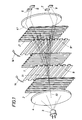
- a scale phase grating running through the length or the circumference of a measuring range has a scanning phase grating 2, 2 ', at least one light source 3 and one collimator 4, 4', with photodetectors 5, and 7, 8 being present.
- the light source 3 can be an LED, LD, incandescent lamp or a laser.
- Scale 1 is a reflective scale with a specific ridge-groove ratio.
- the scanning grating 2, 2 ' has a ridge-furrow ratio which differs significantly from 1: 1.
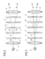
- a leading phase grating 9, 9 ' is attached between the scanning grating 2, 2' and the scale 1. That has, for example, a ridge-furrow ratio of 1: 1 at a furrow depth corresponding to the wavelength of the light used, so that it predominantly +1 in the directions of diffraction. and -1. Order bends.
- the light collimated at the collimator 4 (light beam 10) is first diffracted at the scanning phase grating 2 and the resulting simple light bundle 11 is now divided into two partial beam areas 12, 13 (only in FIG. 2) during the first passage through the guide phase grating 9 ) fanned out, which fall with a small center distance from one another on the scale phase grating 1 and are reflected back by this with diffraction to the grating 9 ', are bent again here and after further diffraction on the scanning phase grating 2' via the collimator 4 'the photo receivers 5, Illuminate 6 or 7, 8.
- the photodetectors 5 and 6 and 7 and 8 receive the interferences of the partial beams 12, 13 diffracted in their direction, which in each of the two pairs 5, 6 and 7, 8 have a nominal offset of 180 ° relative to one another.
- the nominal offset of the signals generated in pairs 5, 6 and 7, 8 compared to the signals of the other pair is 90 °.
- the antiparallel connection can be turned by 180 ° set signals from the photodetectors 5, 7 and 6, 8 generate two 90 ° mutually phase-shifted in the basic form sinusoidal analog measurement signals, in which the one signal is dependent on the adjustment direction with relative adjustment of the scanning unit containing the parts 2 to 9 compared to the scale 1 - or lags behind, so that these signals can be used to control counting or control devices depending on the adjustment direction.
- the leading phase grating can be set to rotate about an axis running normally to its main plane.
- the division of the partial beams 12, 13 and the center distance of their impingement points on the scale phase grating 1 is changed and, subsequently, the phase distance of the signals generated at the receivers 5 to 8 is influenced.
- the rotary adjustment of the leading-phase grating 9 can take place when the measuring system is being installed.
- a relative setting between the grids 2, 1 in the direction of the main axis, that is to say normal to the grating plane would also be conceivable.
Landscapes
- Physics & Mathematics (AREA)
- General Physics & Mathematics (AREA)
- Optical Transform (AREA)
Applications Claiming Priority (2)
| Application Number | Priority Date | Filing Date | Title |
|---|---|---|---|
| AT0008393A AT404637B (de) | 1993-01-21 | 1993-01-21 | Photoelektrische positionsmesseinrichtung |
| AT83/93 | 1993-01-21 |
Publications (3)
| Publication Number | Publication Date |
|---|---|
| EP0608209A2 true EP0608209A2 (fr) | 1994-07-27 |
| EP0608209A3 EP0608209A3 (en) | 1994-09-07 |
| EP0608209B1 EP0608209B1 (fr) | 1997-10-08 |
Family
ID=3481082
Family Applications (1)
| Application Number | Title | Priority Date | Filing Date |
|---|---|---|---|
| EP94890010A Expired - Lifetime EP0608209B1 (fr) | 1993-01-21 | 1994-01-14 | Dispositif photo-électrique pour mesurer la position |
Country Status (4)
| Country | Link |
|---|---|
| US (1) | US5450199A (fr) |
| EP (1) | EP0608209B1 (fr) |
| AT (1) | AT404637B (fr) |
| DE (1) | DE59404236D1 (fr) |
Cited By (1)
| Publication number | Priority date | Publication date | Assignee | Title |
|---|---|---|---|---|
| WO2009144057A1 (fr) * | 2008-05-31 | 2009-12-03 | Dr. Johannes Heidenhain Gmbh | Dispositif de mesure de position optique |
Families Citing this family (12)
| Publication number | Priority date | Publication date | Assignee | Title |
|---|---|---|---|---|
| DE69324532T2 (de) * | 1992-07-15 | 1999-09-23 | Nikon Corp | Lichtquelle für ein Heterodyninterferometer |
| US5532860A (en) * | 1995-03-20 | 1996-07-02 | General Electric Company | Spatial synchronization for optical communication system |
| US5754295A (en) * | 1996-12-20 | 1998-05-19 | Microe, Inc. | Non-contacting torque sensor and displacement measuring apparatus and method |
| US6744520B2 (en) * | 2002-03-04 | 2004-06-01 | Industrial Technology Research Institute | Method for measuring two-dimensional displacement using conjugate optics |
| US7492442B2 (en) * | 2004-08-27 | 2009-02-17 | Asml Holding N.V. | Adjustable resolution interferometric lithography system |
| GB0509727D0 (en) * | 2005-05-13 | 2005-06-22 | Renishaw Plc | Method and apparatus for scale manufacture |
| US20070096646A1 (en) * | 2005-10-28 | 2007-05-03 | Van Nice Harold L | Electroluminescent displays |
| JP6386337B2 (ja) * | 2014-10-23 | 2018-09-05 | 株式会社ミツトヨ | 光学式エンコーダ |
| US10126560B2 (en) * | 2016-02-18 | 2018-11-13 | National Engineering Research Center for Optical Instrumentation | Spectrum-generation system based on multiple-diffraction optical phasometry |
| JP2019086296A (ja) * | 2017-11-01 | 2019-06-06 | 株式会社ミツトヨ | 光学式エンコーダおよびこれを備えた測定器 |
| WO2019125306A1 (fr) * | 2017-12-21 | 2019-06-27 | Agency For Science, Technology And Research | Dispositif optique et son procédé de formation |
| CN113175881B (zh) * | 2021-04-10 | 2022-06-03 | 西安交通大学 | 一种提高光栅读数间隙容差的测量装置 |
Citations (2)
| Publication number | Priority date | Publication date | Assignee | Title |
|---|---|---|---|---|
| JPS57169613A (en) * | 1981-04-13 | 1982-10-19 | Tokyo Optical Co Ltd | Photoelectric encoder |
| EP0509979A2 (fr) * | 1991-04-18 | 1992-10-21 | RSF-Elektronik Gesellschaft m.b.H. | Dispositif de mesure de positions photo-électronique |
Family Cites Families (10)
| Publication number | Priority date | Publication date | Assignee | Title |
|---|---|---|---|---|
| US2886718A (en) * | 1955-05-31 | 1959-05-12 | Ferranti Ltd | Measuring apparatus |
| DE2431551C2 (de) * | 1974-07-01 | 1981-09-17 | Ernst Leitz Wetzlar Gmbh, 6330 Wetzlar | Anordnung zur Messung von Bewegungen und Geschwindigkeiten |
| US4049965A (en) * | 1975-03-06 | 1977-09-20 | National Research Development Corporation | Measurement apparatus |
| US4231662A (en) * | 1978-09-07 | 1980-11-04 | Pitney Bowes Inc. | Phase shift correction for displacement measuring systems using quadrature |
| DE3541199C1 (de) * | 1985-11-21 | 1987-06-25 | Heidenhain Gmbh Dr Johannes | Lichtelektrische Positionsmesseinrichtung |
| FR2615281B1 (fr) * | 1987-05-11 | 1996-08-23 | Canon Kk | Dispositif de mesure d'une distance en mouvement relatif de deux objets mobiles l'un par rapport a l'autre |
| US5064290A (en) * | 1987-12-12 | 1991-11-12 | Renishaw Plc | Opto-electronic scale-reading apparatus wherein phase-separated secondary orders of diffraction are generated |
| JPH0625675B2 (ja) * | 1989-08-30 | 1994-04-06 | オ−クマ株式会社 | 平均化回折モアレ位置検出器 |
| EP0482224B1 (fr) * | 1990-10-20 | 1994-01-12 | Dr. Johannes Heidenhain GmbH | Dispositif interférentiel de mesure pour au moins une direction de mesure |
| DE4132941C2 (de) * | 1990-10-20 | 1994-02-24 | Heidenhain Gmbh Dr Johannes | Interferentielle Meßeinrichtung für wenigstens eine Meßrichtung |
-
1993
- 1993-01-21 AT AT0008393A patent/AT404637B/de not_active IP Right Cessation
-
1994
- 1994-01-14 EP EP94890010A patent/EP0608209B1/fr not_active Expired - Lifetime
- 1994-01-14 DE DE59404236T patent/DE59404236D1/de not_active Expired - Lifetime
- 1994-01-18 US US08/184,254 patent/US5450199A/en not_active Expired - Lifetime
Patent Citations (2)
| Publication number | Priority date | Publication date | Assignee | Title |
|---|---|---|---|---|
| JPS57169613A (en) * | 1981-04-13 | 1982-10-19 | Tokyo Optical Co Ltd | Photoelectric encoder |
| EP0509979A2 (fr) * | 1991-04-18 | 1992-10-21 | RSF-Elektronik Gesellschaft m.b.H. | Dispositif de mesure de positions photo-électronique |
Non-Patent Citations (2)
| Title |
|---|
| Dissertation von J. Wilhelm Aufnehmer zur Messung von Lage{nderungen TU Hannover 1978 * |
| PATENT ABSTRACTS OF JAPAN vol. 7, no. 10 (P-168) (1155) 14. Januar 1983 & JP-A-57 169 613 (TOUKIYOU KOUGAKU KIKAI K.K.) 19. Oktober 1982 * |
Cited By (3)
| Publication number | Priority date | Publication date | Assignee | Title |
|---|---|---|---|---|
| WO2009144057A1 (fr) * | 2008-05-31 | 2009-12-03 | Dr. Johannes Heidenhain Gmbh | Dispositif de mesure de position optique |
| DE102008025870A1 (de) | 2008-05-31 | 2009-12-03 | Dr. Johannes Heidenhain Gmbh | Optische Positionsmesseinrichtung |
| US8537370B2 (en) | 2008-05-31 | 2013-09-17 | Dr. Johannes Heidenhain Gmbh | Optical position measuring device |
Also Published As
| Publication number | Publication date |
|---|---|
| AT404637B (de) | 1999-01-25 |
| EP0608209A3 (en) | 1994-09-07 |
| ATA8393A (de) | 1998-05-15 |
| EP0608209B1 (fr) | 1997-10-08 |
| US5450199A (en) | 1995-09-12 |
| DE59404236D1 (de) | 1997-11-13 |
Similar Documents
| Publication | Publication Date | Title |
|---|---|---|
| EP0163824B1 (fr) | Dispositif de mesure photo-électrique | |
| EP0509979B1 (fr) | Dispositif de mesure de positions photo-électronique | |
| DE3700906C2 (de) | Verschlüßler | |
| EP1923673B1 (fr) | Dispositif de mesure de position | |
| DE3541199C1 (de) | Lichtelektrische Positionsmesseinrichtung | |
| EP0608209B1 (fr) | Dispositif photo-électrique pour mesurer la position | |
| DE10132521A1 (de) | Positionsmesseinrichtung | |
| DE60033075T3 (de) | Kodierer | |
| DE4041584A1 (de) | Interferentielle messeinrichtung fuer wenigstens eine messrichtung | |
| DE10325082B4 (de) | Fotoelektrischer Drehwertgeber | |
| EP0747674B1 (fr) | Dispositif photo-électrique de mesure de positions | |
| EP0365806B1 (fr) | Dispositif de mesure de position angulaire | |
| EP1524503B1 (fr) | Codeur optique | |
| EP0754933B1 (fr) | Dispositif de mesure de positions | |
| EP1028309A1 (fr) | Codeur optique | |
| DE102004041950A1 (de) | Optische Positionsmesseinrichtung | |
| EP3936830B1 (fr) | Dispositif optique de mesure de la position | |
| EP0517690B1 (fr) | Système de mesure incrémentale | |
| WO1998016802A1 (fr) | Indicateur optique de position | |
| DE19957777A1 (de) | Optische Positionsmeßeinrichtung | |
| DE19614466B4 (de) | Signalverarbeitungsanordnung für eine Positionsmeßeinrichtung | |
| DE8532808U1 (de) | Lichtelektrische Positionsmeßeinrichtung | |
| DE9011628U1 (de) | Optoelektronische Anordnung zum Abtasten von Codeträgern | |
| DE9218009U1 (de) | Winkelmeßeinrichtung | |
| EP0419701A1 (fr) | Dispositif pour la mesure d'angles |
Legal Events
| Date | Code | Title | Description |
|---|---|---|---|
| PUAI | Public reference made under article 153(3) epc to a published international application that has entered the european phase |
Free format text: ORIGINAL CODE: 0009012 |
|
| PUAL | Search report despatched |
Free format text: ORIGINAL CODE: 0009013 |
|
| AK | Designated contracting states |
Kind code of ref document: A2 Designated state(s): BE CH DE FR GB IT LI LU NL SE |
|
| AK | Designated contracting states |
Kind code of ref document: A3 Designated state(s): BE CH DE FR GB IT LI LU NL SE |
|
| 17P | Request for examination filed |
Effective date: 19940916 |
|
| 17Q | First examination report despatched |
Effective date: 19960905 |
|
| GRAG | Despatch of communication of intention to grant |
Free format text: ORIGINAL CODE: EPIDOS AGRA |
|
| GRAH | Despatch of communication of intention to grant a patent |
Free format text: ORIGINAL CODE: EPIDOS IGRA |
|
| GRAH | Despatch of communication of intention to grant a patent |
Free format text: ORIGINAL CODE: EPIDOS IGRA |
|
| GRAA | (expected) grant |
Free format text: ORIGINAL CODE: 0009210 |
|
| AK | Designated contracting states |
Kind code of ref document: B1 Designated state(s): BE CH DE FR GB IT LI LU NL SE |
|
| PG25 | Lapsed in a contracting state [announced via postgrant information from national office to epo] |
Ref country code: NL Free format text: LAPSE BECAUSE OF FAILURE TO SUBMIT A TRANSLATION OF THE DESCRIPTION OR TO PAY THE FEE WITHIN THE PRESCRIBED TIME-LIMIT Effective date: 19971008 |
|
| REG | Reference to a national code |
Ref country code: CH Ref legal event code: NV Representative=s name: DIPL.-ING. W. STEUDTNER Ref country code: CH Ref legal event code: EP |
|
| ET | Fr: translation filed | ||
| GBT | Gb: translation of ep patent filed (gb section 77(6)(a)/1977) |
Effective date: 19971021 |
|
| REF | Corresponds to: |
Ref document number: 59404236 Country of ref document: DE Date of ref document: 19971113 |
|
| ITF | It: translation for a ep patent filed |
Owner name: STUDIO CONS. BREVETTUALE S.R.L. |
|
| PG25 | Lapsed in a contracting state [announced via postgrant information from national office to epo] |
Ref country code: SE Effective date: 19980108 |
|
| PG25 | Lapsed in a contracting state [announced via postgrant information from national office to epo] |
Ref country code: LU Free format text: LAPSE BECAUSE OF NON-PAYMENT OF DUE FEES Effective date: 19980114 |
|
| PG25 | Lapsed in a contracting state [announced via postgrant information from national office to epo] |
Ref country code: BE Free format text: LAPSE BECAUSE OF NON-PAYMENT OF DUE FEES Effective date: 19980131 |
|
| NLV1 | Nl: lapsed or annulled due to failure to fulfill the requirements of art. 29p and 29m of the patents act | ||
| BERE | Be: lapsed |
Owner name: RSF-ELEKTRONIK G.M.B.H. Effective date: 19980131 |
|
| PLBE | No opposition filed within time limit |
Free format text: ORIGINAL CODE: 0009261 |
|
| STAA | Information on the status of an ep patent application or granted ep patent |
Free format text: STATUS: NO OPPOSITION FILED WITHIN TIME LIMIT |
|
| 26N | No opposition filed | ||
| REG | Reference to a national code |
Ref country code: GB Ref legal event code: IF02 |
|
| REG | Reference to a national code |
Ref country code: CH Ref legal event code: PCAR Free format text: PATENTANWALTSBUREAU STEUDTNER;AHORNWEG 12;5702 NIEDERLENZ (CH) |
|
| PGFP | Annual fee paid to national office [announced via postgrant information from national office to epo] |
Ref country code: IT Payment date: 20080125 Year of fee payment: 15 |
|
| PGFP | Annual fee paid to national office [announced via postgrant information from national office to epo] |
Ref country code: FR Payment date: 20080111 Year of fee payment: 15 |
|
| PGFP | Annual fee paid to national office [announced via postgrant information from national office to epo] |
Ref country code: GB Payment date: 20090122 Year of fee payment: 16 Ref country code: CH Payment date: 20090115 Year of fee payment: 16 |
|
| REG | Reference to a national code |
Ref country code: FR Ref legal event code: ST Effective date: 20091030 |
|
| PG25 | Lapsed in a contracting state [announced via postgrant information from national office to epo] |
Ref country code: FR Free format text: LAPSE BECAUSE OF NON-PAYMENT OF DUE FEES Effective date: 20090202 |
|
| PGFP | Annual fee paid to national office [announced via postgrant information from national office to epo] |
Ref country code: DE Payment date: 20100121 Year of fee payment: 17 |
|
| REG | Reference to a national code |
Ref country code: CH Ref legal event code: PL |
|
| GBPC | Gb: european patent ceased through non-payment of renewal fee |
Effective date: 20100114 |
|
| PG25 | Lapsed in a contracting state [announced via postgrant information from national office to epo] |
Ref country code: LI Free format text: LAPSE BECAUSE OF NON-PAYMENT OF DUE FEES Effective date: 20100131 Ref country code: CH Free format text: LAPSE BECAUSE OF NON-PAYMENT OF DUE FEES Effective date: 20100131 |
|
| PG25 | Lapsed in a contracting state [announced via postgrant information from national office to epo] |
Ref country code: GB Free format text: LAPSE BECAUSE OF NON-PAYMENT OF DUE FEES Effective date: 20100114 |
|
| PG25 | Lapsed in a contracting state [announced via postgrant information from national office to epo] |
Ref country code: IT Free format text: LAPSE BECAUSE OF NON-PAYMENT OF DUE FEES Effective date: 20090114 |
|
| REG | Reference to a national code |
Ref country code: DE Ref legal event code: R119 Ref document number: 59404236 Country of ref document: DE Effective date: 20110802 |
|
| PG25 | Lapsed in a contracting state [announced via postgrant information from national office to epo] |
Ref country code: DE Free format text: LAPSE BECAUSE OF NON-PAYMENT OF DUE FEES Effective date: 20110802 |