EP0608091B1 - Pulsed power converter with multiple output voltages - Google Patents
Pulsed power converter with multiple output voltages Download PDFInfo
- Publication number
- EP0608091B1 EP0608091B1 EP94300295A EP94300295A EP0608091B1 EP 0608091 B1 EP0608091 B1 EP 0608091B1 EP 94300295 A EP94300295 A EP 94300295A EP 94300295 A EP94300295 A EP 94300295A EP 0608091 B1 EP0608091 B1 EP 0608091B1
- Authority
- EP
- European Patent Office
- Prior art keywords
- transformer
- module
- coupled
- storage capacitor
- energy storage
- Prior art date
- Legal status (The legal status is an assumption and is not a legal conclusion. Google has not performed a legal analysis and makes no representation as to the accuracy of the status listed.)
- Expired - Lifetime
Links
- 239000003990 capacitor Substances 0.000 claims description 49
- 238000004146 energy storage Methods 0.000 claims description 47
- 238000004804 winding Methods 0.000 claims description 44
- 238000001914 filtration Methods 0.000 claims description 20
- 230000001105 regulatory effect Effects 0.000 claims description 15
- 239000004020 conductor Substances 0.000 claims description 6
- 230000008878 coupling Effects 0.000 claims description 6
- 238000010168 coupling process Methods 0.000 claims description 6
- 238000005859 coupling reaction Methods 0.000 claims description 6
- 101150013999 CRBN gene Proteins 0.000 description 1
- 101150016677 ohgt gene Proteins 0.000 description 1
Images
Classifications
-
- H—ELECTRICITY
- H02—GENERATION; CONVERSION OR DISTRIBUTION OF ELECTRIC POWER
- H02M—APPARATUS FOR CONVERSION BETWEEN AC AND AC, BETWEEN AC AND DC, OR BETWEEN DC AND DC, AND FOR USE WITH MAINS OR SIMILAR POWER SUPPLY SYSTEMS; CONVERSION OF DC OR AC INPUT POWER INTO SURGE OUTPUT POWER; CONTROL OR REGULATION THEREOF
- H02M3/00—Conversion of DC power input into DC power output
- H02M3/22—Conversion of DC power input into DC power output with intermediate conversion into AC
- H02M3/24—Conversion of DC power input into DC power output with intermediate conversion into AC by static converters
- H02M3/28—Conversion of DC power input into DC power output with intermediate conversion into AC by static converters using discharge tubes with control electrode or semiconductor devices with control electrode to produce the intermediate AC
- H02M3/325—Conversion of DC power input into DC power output with intermediate conversion into AC by static converters using discharge tubes with control electrode or semiconductor devices with control electrode to produce the intermediate AC using devices of a triode or a transistor type requiring continuous application of a control signal
- H02M3/335—Conversion of DC power input into DC power output with intermediate conversion into AC by static converters using discharge tubes with control electrode or semiconductor devices with control electrode to produce the intermediate AC using devices of a triode or a transistor type requiring continuous application of a control signal using semiconductor devices only
- H02M3/33561—Conversion of DC power input into DC power output with intermediate conversion into AC by static converters using discharge tubes with control electrode or semiconductor devices with control electrode to produce the intermediate AC using devices of a triode or a transistor type requiring continuous application of a control signal using semiconductor devices only having more than one ouput with independent control
Definitions
- the present invention relates generally to power converters and, more particularly, to power converters for supplying distributed pulsed loads such as, for example, in radar applications.
- T/R phased-array radar transmit/receive
- RF radio frequency
- these voltages include at least one pulsed voltage and several low utilization voltages. Normally, the low utilization voltages are brought into the T/R module via separate lines. Energy storage for the pulsed line is external to the T/R module and is furthermore at a low utilization voltage, resulting in the need for relatively large high-energy-storage capacitors.
- typical T/R modules have many module pins and hence complicated configurations.
- a phased-array apparatus including plural TR modules, each TR module including at least an RF amplifier and controls, said apparatus comprising:
- a distributed power system for providing multiple output voltages, including pulsed voltages, to a solid-state phased-array radar T/R module comprises: an energy-storage capacitor for coupling to an input dc power source and for storing substantial energy at high voltage for supplying pulsed voltages at low voltage; at least one capacitance-multiplying converter, including first and second transformers with multiple secondary windings, for producing positive and negative voltages on buses internal to a power module; and a plurality of series regulators to obtain multiple positive and negative load voltages, including pulsed voltages, from the positive and negative bus voltages.
- substantial energy storage is achieved within the power module; and, if even more energy storage is desired, an additional external energy-storage capacitor can be coupled to the input power leads, thereby being coupled in parallel with the energy-storage capacitor. Only two power pins are needed to supply the entire module.
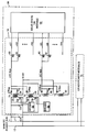
- Figure 1 schematically illustrates a multiple-output pulsed power supply according to the present invention.
- the multiple-output pulsed power supply of Figure 1 is shown as being employed in a radar application; however, it is to be understood that the power supply is suitable for any application having distributed pulsed loads.
- the power module includes a capacitance-multiplying converter 20 which comprises a series combination of a first switching device Qa and a primary winding 22 of a first transformer T1 coupled in parallel with an energy-storage capacitor Ce.
- a secondary winding 24 of transformer T1 is coupled in parallel, via a diode rectifier CRap, to a small high-frequency output filter capacitor Cop.
- Capacitance-multiplying converter 20 further includes a series combination of a second switching device Qb and a primary winding 26 of a second transformer T2 also coupled in parallel with energy-storage capacitor Ce.
- Switching devices Qa and Qb are illustrated as FET's; however, any suitable types of switching devices may be used.
- a secondary winding 28 of transformer T2 is coupled in parallel, via a diode rectifier CRbp, to output filter capacitor Cop.
- Transformers T1 and T2 have substantially the same turns ratio N.
- Capacitance-multiplying converter 20 is also illustrated as including additional secondary windings 40 and 42 of transformers T1 and T2, respectively. Additional secondary windings 40 and 42 are coupled via diode rectifiers CRan and CRbn, respectively, to an output filter capacitor Con and the negative dc bus voltage.
- Output voltages +V1, +V2, ... are obtained from the positive dc bus voltage via series regulators 50, 51 ..., respectively, to a solid-state phased-array radar T/R module 54.
- Output voltages -V1, -V2, ...-Vm are obtained from the negative dc bus voltage via series regulators 60 and 61 ..., respectively, to solid-state radar T/R module 54.
- +V1 is a pulsed voltage
- the remaining output voltages +V2 ...+Vn and -V2...-Vm are bias voltages used for control and receive functions.
- switching devices Qa and Qb are gated 180° out-of-phase with a 50% duty cycle by drive means 55. Hence, because one of the switching devices is always conducting, the energy-storage capacitor Ce is always transformer-coupled to the positive and negative dc output buses.
- the output filter capacitors Cop and Con are used for filtering switching noise and hence are not required to store substantial energy.
- module 10 may be coupled to dc power buses 11 and 12 and operate in the same manner as module 10.
- the energy storage capacitor is connected across the input power lines to the capacitance-multiplying converter such that, if additional energy storage is needed, another energy-storage capacitor (shown as capacitor Cin in Figure 1) can be connected directly across the input lines to converter 20, the additional energy-storage capacitor Cin thus being coupled in parallel with energy-storage capacitor Ce.
- capacitor Cin another energy-storage capacitor
- the low multiple utilization voltages required in a radar T/R module are generated while requiring only two power module input pins.
- pulse energy is stored in a high-voltage capacitor rather than at the substantially lower utilization voltages, thereby minimizing capacitor volume, allowing substantial energy storage to be in the module itself.
- the number of magnetic components is minimized, and operation at high frequencies is possible, thereby reducing module size.
- the entire power supply can be embedded in the T/R module with the load, as indicated by dashed line 80, with only two power leads into module 80 being required.
Landscapes
- Engineering & Computer Science (AREA)
- Power Engineering (AREA)
- Dc-Dc Converters (AREA)
- Direct Current Feeding And Distribution (AREA)
- Radar Systems Or Details Thereof (AREA)
Description
Claims (2)
- A phased-array apparatus including plural TR modules (54), each TR module including at least an RF amplifier and controls, said apparatus comprising:a two-conductor DC power bus (11,12) carrying power at a particular voltage;a plurality of power supply/TR module assemblages (70,80), each comprising a power module (10) and an associated TR module (54);each said TR module (54) including at least first and second power input ports, and requiring for operation of said amplifier and controls at least first (Vl) and second (V2) regulated voltages, respectively, at said first and second power input ports, and pulse loading at least said first regulated voltage;each said power supply (10) including:(a) an energy storage capacitor (Ce) including first and second electrodes, each of which is coupled directly to a different one of said two conductors of said DC power bus;(b) a first transformer (T1) with primary (22) and secondary (24) windings, the number of turns of said secondary winding of said first transformer being less than the number of turns of said primary winding of said first transformer by a predetermined ratio;(c) a second transformer (T2) with primary (26) and secondary (28) windings, the number of turns of said secondary winding of said second transformer being less than the number of turns of said primary winding of said second transformer by said predetermined ratio;(d) first controllable switching means (Qa) coupled directly to at least one of said first and second electrodes of said energy storage capacitor and to said primary winding (22) of said first transformer (T1), for controllably coupling said primary winding of said first transformer across said energy storage capacitor (Ce) during those intervals in which said intervals in which said first switching means is in a first state (conductive), and for controllably decoupling said primary winding of said first transformer from said energy storage capacitor during those intervals in which said first controllable switching means is in a second (nonconductive) state;(e) second controllable switching means (Qb) coupled, by a path lacking inductors, to at least one of said first and second electrodes of said energy storage capacitor and to said primary winding (26) of said second transformer (T2), for controllably coupling said primary winding of said second transformer across said energy storage capacitor (Ce) during those intervals in which said second switching means is in said first state (conductive), and for controllably decoupling said primary winding of said second transformer from said energy storage capacitor during those intervals in which said second controllable switching means is in said second state (nonconductive);(f) switch drive means (55) coupled to said first and second switching means, for gating said first and second switching means mutually out-of-phase and with a 50% duty cycle;(g) noise filtering capacitance means (Cop);(h) first rectifying means (CRap) coupled directly to said secondary winding (24) of said first transformer (T1) and to said noise filtering capacitance means (Cop), and poled for aiding in producing a first unregulated DC voltage across said noise filtering capacitance means during those intervals in which said primary winding of said first transformer is coupled across said energy storage capacitor (Ce) by said first switching means in said first (conductive) state;(i) second rectifying means (CRbp) coupled to said secondary winding (26) of said second transformer (T2) and to said noise filtering capacitance means (Cop) by a path lacking inductors, and poled for aiding in producing said first unregulated DC voltage across said noise filtering capacitance means during those intervals in which said primary winding of said second transformer is coupled across said energy storage capacitor (Ce) by said second switching means in said first (conductive) state;(j) first series voltage regulation means (50) coupled directly to said noise suppressing capacitance means (Cop) and to said first power input port (V1) of said TR module (54), for generating a first regulated voltage at said first power input port (V1) of said TR module;(k) second series voltage regulation means (51) coupled directly to said noise suppressing capacitance means (Cop) and to said second power input port (V2) of said TR module (54), for generating a second regulated voltage at said second power input port (V2) of said TR module;(l) whereby said first and second transformers are alternately coupled to said energy storage capacitor by said first and second switching means and said noise filtering capacitance means is continuously coupled by a capacitance multiplying turns ratio of one of said first and second transformers to said energy storage capacitor, and said pulse load of said TR module is supplied by said energy storage capacitor by way of that one of said first and second transformers currently coupled between said energy storage capacitor and said noise filtering capacitance means.
- An apparatus according to claim 1, wherein:each said TR module (54) includes at least third and fourth power input ports, and requires for its operation at least third (-V1) and fourth (-V2) regulated voltages, respectively, at said first and second power input ports, which third and fourth regulated voltages are poled oppositely to said first regulated voltage; andeach of said first and second transformers includes a further secondary winding (40,42), and further comprising:second noise filtering capacitance means (Con);third rectifying means (CRan) coupled to said further secondary winding (40) of said first transformer (T1) and to said second noise filtering capacitance means (Con) by a path lacking inductors, and poled for aiding in producing a second unregulated DC voltage, opposite to said first unregulated DC voltage, across said second noise filtering capacitance means during those intervals in which said primary winding of said first transformer is coupled across said energy storage capacitor (Ce) by said first switching means in said first (conductive) state;fourth rectifying means (CRbn) coupled to said further secondary winding (42) of said second transformer (T2) and to said second noise filtering capacitance means (Con) by a path lacking inductors, and poled for aiding in producing said second unregulated DC voltage across said second noise filtering capacitance means during those intervals in which said primary winding of said second transformer is coupled across said energy storage capacitor (Ce) by said second switching means in said first (conductive) state;third series regulation means (60) coupled to said second noise suppressing capacitance means (Con) and to said third power input port (-V1) of said TR module (54) by a path lacking inductors, for generating a third regulated voltage at said third power input port (-V1) of said TR module;fourth series regulation means (61) coupled to said second noise suppressing capacitance means (Con) and to said fourth power input port (-V2) of said TR module (54) by a path lacking inductors, for generating a fourth regulated voltage at said fourth power input port (-V2) of said TR module, whereby said four regulated voltages are applied to said TR module while drawing power from said two-conductor DC power bus only by way of said coupling of said energy storage capacitor (Ce) electrodes coupled to said conductors of said DC power bus.
Applications Claiming Priority (2)
| Application Number | Priority Date | Filing Date | Title |
|---|---|---|---|
| US595293 | 1993-01-19 | ||
| US08/005,952 US5377090A (en) | 1993-01-19 | 1993-01-19 | Pulsed power converter with multiple output voltages |
Publications (3)
| Publication Number | Publication Date |
|---|---|
| EP0608091A2 EP0608091A2 (en) | 1994-07-27 |
| EP0608091A3 EP0608091A3 (en) | 1996-03-13 |
| EP0608091B1 true EP0608091B1 (en) | 2000-10-25 |
Family
ID=21718532
Family Applications (1)
| Application Number | Title | Priority Date | Filing Date |
|---|---|---|---|
| EP94300295A Expired - Lifetime EP0608091B1 (en) | 1993-01-19 | 1994-01-17 | Pulsed power converter with multiple output voltages |
Country Status (4)
| Country | Link |
|---|---|
| US (1) | US5377090A (en) |
| EP (1) | EP0608091B1 (en) |
| JP (1) | JPH06261451A (en) |
| DE (1) | DE69426162T2 (en) |
Families Citing this family (53)
| Publication number | Priority date | Publication date | Assignee | Title |
|---|---|---|---|---|
| US5617015A (en) * | 1995-06-07 | 1997-04-01 | Linear Technology Corporation | Multiple output regulator with time sequencing |
| JP2002514378A (en) | 1997-01-24 | 2002-05-14 | シンクォール・インコーポレーテッド | High efficiency power converter |
| US7269034B2 (en) | 1997-01-24 | 2007-09-11 | Synqor, Inc. | High efficiency power converter |
| ES2150377B1 (en) * | 1998-07-31 | 2001-06-01 | Univ Madrid Carlos Iii | CONVERTERS OF CONTINUOUS-CONTINUOUS POWER OF MULTIPLE OUTPUTS. |
| JP3280635B2 (en) * | 1999-04-21 | 2002-05-13 | 長野日本無線株式会社 | Energy transfer device and power storage system |
| JP3280641B2 (en) * | 1999-09-08 | 2002-05-13 | 長野日本無線株式会社 | Energy transfer device |
| US6205036B1 (en) * | 1999-04-21 | 2001-03-20 | Nagano Japan Radio Co., Ltd. | Energy transfer unit, charge unit, and power supply unit |
| US6813318B1 (en) | 1999-04-30 | 2004-11-02 | Rosemount Inc, | Process transmitter having a step-up converter for powering analog components |
| SG122734A1 (en) * | 1999-07-23 | 2006-06-29 | Walter Roland Chen | AC/DC adapter 110/230 volts, with multiple dc outputs |
| SE0102303D0 (en) * | 2001-06-27 | 2001-06-27 | Ericsson Telefon Ab L M | DC / DC converter |
| US6949916B2 (en) | 2002-11-12 | 2005-09-27 | Power-One Limited | System and method for controlling a point-of-load regulator |
| US7000125B2 (en) * | 2002-12-21 | 2006-02-14 | Power-One, Inc. | Method and system for controlling and monitoring an array of point-of-load regulators |
| US7394445B2 (en) | 2002-11-12 | 2008-07-01 | Power-One, Inc. | Digital power manager for controlling and monitoring an array of point-of-load regulators |
| US7049798B2 (en) * | 2002-11-13 | 2006-05-23 | Power-One, Inc. | System and method for communicating with a voltage regulator |
| US7456617B2 (en) | 2002-11-13 | 2008-11-25 | Power-One, Inc. | System for controlling and monitoring an array of point-of-load regulators by a host |
| US6833691B2 (en) * | 2002-11-19 | 2004-12-21 | Power-One Limited | System and method for providing digital pulse width modulation |
| US7249267B2 (en) | 2002-12-21 | 2007-07-24 | Power-One, Inc. | Method and system for communicating filter compensation coefficients for a digital power control system |
| US7737961B2 (en) | 2002-12-21 | 2010-06-15 | Power-One, Inc. | Method and system for controlling and monitoring an array of point-of-load regulators |
| US7836322B2 (en) | 2002-12-21 | 2010-11-16 | Power-One, Inc. | System for controlling an array of point-of-load regulators and auxiliary devices |
| US7673157B2 (en) | 2002-12-21 | 2010-03-02 | Power-One, Inc. | Method and system for controlling a mixed array of point-of-load regulators through a bus translator |
| US7882372B2 (en) | 2002-12-21 | 2011-02-01 | Power-One, Inc. | Method and system for controlling and monitoring an array of point-of-load regulators |
| US7266709B2 (en) | 2002-12-21 | 2007-09-04 | Power-One, Inc. | Method and system for controlling an array of point-of-load regulators and auxiliary devices |
| US7743266B2 (en) | 2002-12-21 | 2010-06-22 | Power-One, Inc. | Method and system for optimizing filter compensation coefficients for a digital power control system |
| US6933709B2 (en) * | 2003-02-10 | 2005-08-23 | Power-One Limited | Digital control system and method for switched mode power supply |
| US7373527B2 (en) * | 2002-12-23 | 2008-05-13 | Power-One, Inc. | System and method for interleaving point-of-load regulators |
| US7710092B2 (en) | 2003-02-10 | 2010-05-04 | Power-One, Inc. | Self tracking ADC for digital power supply control systems |
| US7023190B2 (en) * | 2003-02-10 | 2006-04-04 | Power-One, Inc. | ADC transfer function providing improved dynamic regulation in a switched mode power supply |
| US6936999B2 (en) | 2003-03-14 | 2005-08-30 | Power-One Limited | System and method for controlling output-timing parameters of power converters |
| US7080265B2 (en) | 2003-03-14 | 2006-07-18 | Power-One, Inc. | Voltage set point control scheme |
| US6788036B1 (en) | 2003-03-28 | 2004-09-07 | Ower-One Limited | Method and system for current sharing among a plurality of power modules |
| JP3851303B2 (en) * | 2003-09-08 | 2006-11-29 | ローム株式会社 | Multi-output type power supply device and portable device using the same |
| US6958592B2 (en) * | 2003-11-26 | 2005-10-25 | Power-One, Inc. | Adaptive delay control circuit for switched mode power supply |
| US7372682B2 (en) | 2004-02-12 | 2008-05-13 | Power-One, Inc. | System and method for managing fault in a power system |
| US7187158B2 (en) * | 2004-04-15 | 2007-03-06 | Rosemount, Inc. | Process device with switching power supply |
| US20050286709A1 (en) * | 2004-06-28 | 2005-12-29 | Steve Horton | Customer service marketing |
| US7141956B2 (en) * | 2005-03-18 | 2006-11-28 | Power-One, Inc. | Digital output voltage regulation circuit having first control loop for high speed and second control loop for high accuracy |
| US7554310B2 (en) | 2005-03-18 | 2009-06-30 | Power-One, Inc. | Digital double-loop output voltage regulation |
| US7239115B2 (en) | 2005-04-04 | 2007-07-03 | Power-One, Inc. | Digital pulse width modulation controller with preset filter coefficients |
| US7327149B2 (en) | 2005-05-10 | 2008-02-05 | Power-One, Inc. | Bi-directional MOS current sense circuit |
| JP4692155B2 (en) * | 2005-08-25 | 2011-06-01 | サンケン電気株式会社 | Switching power supply |
| US7868485B2 (en) * | 2005-10-25 | 2011-01-11 | Hamilton Sundstrand Corporation | Pulsed power supply with current ripple reduction |
| WO2008141802A1 (en) * | 2007-05-22 | 2008-11-27 | Tyco Electronics Amp Gmbh | Power supply unit and power supply and communication sytem in an electromechanical appliance |
| US7834613B2 (en) | 2007-10-30 | 2010-11-16 | Power-One, Inc. | Isolated current to voltage, voltage to voltage converter |
| IL188477A (en) * | 2007-12-27 | 2014-06-30 | Elta Systems Ltd | Power array for high power pulse load |
| US7970063B2 (en) * | 2008-03-10 | 2011-06-28 | Rosemount Inc. | Variable liftoff voltage process field device |
| JP5361447B2 (en) * | 2009-02-26 | 2013-12-04 | 株式会社東芝 | Phased array radar |
| US8786128B2 (en) | 2010-05-11 | 2014-07-22 | Rosemount Inc. | Two-wire industrial process field device with power scavenging |
| US9417315B2 (en) | 2012-12-20 | 2016-08-16 | The Board Of Regents Of The University Of Oklahoma | Radar system and methods for making and using same |
| US10199950B1 (en) | 2013-07-02 | 2019-02-05 | Vlt, Inc. | Power distribution architecture with series-connected bus converter |
| CN103647446B (en) * | 2013-12-03 | 2017-01-18 | 北京中电华大电子设计有限责任公司 | SOC verification platform power supply structure for improving universality and reliability |
| US10862398B2 (en) * | 2015-02-03 | 2020-12-08 | Astec International Limited | DC-DC power converter for use in data communications distributed power architecture |
| CN104953887B (en) * | 2015-07-01 | 2017-05-31 | 中国科学院电工研究所 | A kind of repeated frequency high-voltage square-wave pulse power source |
| US10756632B2 (en) | 2017-06-26 | 2020-08-25 | Bel Fuse (Macao Commerical Offshore) Limited | Power supply with auxiliary converter for extended input voltage range |
Family Cites Families (12)
| Publication number | Priority date | Publication date | Assignee | Title |
|---|---|---|---|---|
| US3614599A (en) * | 1970-09-17 | 1971-10-19 | Superior Electric Co | Three-phase delta-connected voltage-regulating system and method therefor |
| US3660672A (en) * | 1971-02-25 | 1972-05-02 | Pioneer Magnetics Inc | Power supply dual output |
| JPS5129702Y2 (en) * | 1971-06-09 | 1976-07-27 | ||
| US4355884A (en) * | 1979-01-20 | 1982-10-26 | Canon Kabushiki Kaisha | Electrophotographic apparatus |
| DE3369778D1 (en) * | 1982-06-04 | 1987-03-12 | Nippon Chemicon | Power supply device |
| US4586119A (en) * | 1984-04-16 | 1986-04-29 | Itt Corporation | Off-line switching mode power supply |
| JPS63179781U (en) * | 1987-05-13 | 1988-11-21 | ||
| US4788634A (en) * | 1987-06-22 | 1988-11-29 | Massachusetts Institute Of Technology | Resonant forward converter |
| DE3806983C2 (en) * | 1988-03-03 | 1994-07-21 | Siemens Ag | Circuit arrangement for generating voltages of different polarities |
| US4829216A (en) * | 1988-05-16 | 1989-05-09 | Rca Licensing Corporation | SCR regulator for a television apparatus |
| US5013980A (en) * | 1988-11-01 | 1991-05-07 | Thomson Consumer Electronics, Inc. | Voltage regulator in a television apparatus |
| DE4118918A1 (en) * | 1991-06-08 | 1992-12-10 | Philips Patentverwaltung | DC=DC converter with two sec. output stages - has two current-controlled transductor chokes in series supplying one of two rectifying and smoothing circuits |
-
1993
- 1993-01-19 US US08/005,952 patent/US5377090A/en not_active Expired - Lifetime
-
1994
- 1994-01-17 DE DE69426162T patent/DE69426162T2/en not_active Expired - Lifetime
- 1994-01-17 EP EP94300295A patent/EP0608091B1/en not_active Expired - Lifetime
- 1994-01-18 JP JP6003342A patent/JPH06261451A/en active Pending
Also Published As
| Publication number | Publication date |
|---|---|
| DE69426162T2 (en) | 2001-03-29 |
| EP0608091A2 (en) | 1994-07-27 |
| EP0608091A3 (en) | 1996-03-13 |
| JPH06261451A (en) | 1994-09-16 |
| US5377090A (en) | 1994-12-27 |
| DE69426162D1 (en) | 2000-11-30 |
Similar Documents
| Publication | Publication Date | Title |
|---|---|---|
| US5377090A (en) | Pulsed power converter with multiple output voltages | |
| EP0602835B1 (en) | Voltage control circuits | |
| US4777406A (en) | High voltage power supply particularly adapted for a TWT | |
| US5140510A (en) | Constant frequency power converter | |
| DE3650480T2 (en) | Power booster with zero current changeover | |
| US4675797A (en) | Current-fed, forward converter switching at zero current | |
| US5204551A (en) | Method and apparatus for high power pulse modulation | |
| US4860189A (en) | Full bridge power converter circuit | |
| EP0428377B1 (en) | DC/DC switching converter circuit | |
| US5255174A (en) | Regulated bi-directional DC-to-DC voltage converter which maintains a continuous input current during step-up conversion | |
| US5796598A (en) | Voltage-converting circuit for the power supply of an electrical consumer of high output, particularly a bobbin winding machine | |
| US4513361A (en) | Multi-phase DC-to-AC and DC-to-DC boost converter | |
| KR100455651B1 (en) | Multi-output dc/dc voltage converting apparatus and liquid crystal display, including multi-output dc/dc voltage converter for generating main power through choke system and auxiliary power through flyback system | |
| US5038264A (en) | Multiple-output, single-ended, resonant power converter | |
| US20020114172A1 (en) | Converter circuit and method with auxiliary supply voltage | |
| AU602070B2 (en) | A converter circuit with a single-ended blocking converter | |
| US4213173A (en) | Polarity-and-load independent circuit arrangement for converting electrical energy | |
| US5619404A (en) | Multi-channel single stage high power factor AC to DC converter | |
| KR20010014809A (en) | Direct current source circuit | |
| EP1427093A1 (en) | Multi-output dc-dc converter | |
| US5274539A (en) | Capacitance-multiplying converters for supplying distributed pulsed loads | |
| CN111630760B (en) | Modular voltage converter | |
| US5282122A (en) | High voltage power supply topology suited for miniaturization | |
| KR20000057491A (en) | Dual-output dc-dc power supply | |
| WO1991000643A1 (en) | Ac/dc conversion with reduced supply waveform distortion |
Legal Events
| Date | Code | Title | Description |
|---|---|---|---|
| PUAI | Public reference made under article 153(3) epc to a published international application that has entered the european phase |
Free format text: ORIGINAL CODE: 0009012 |
|
| AK | Designated contracting states |
Kind code of ref document: A2 Designated state(s): DE FR GB IT NL |
|
| PUAL | Search report despatched |
Free format text: ORIGINAL CODE: 0009013 |
|
| AK | Designated contracting states |
Kind code of ref document: A3 Designated state(s): DE FR GB IT NL |
|
| RHK1 | Main classification (correction) |
Ipc: H02M 3/337 |
|
| 17P | Request for examination filed |
Effective date: 19960913 |
|
| 17Q | First examination report despatched |
Effective date: 19970127 |
|
| GRAG | Despatch of communication of intention to grant |
Free format text: ORIGINAL CODE: EPIDOS AGRA |
|
| GRAG | Despatch of communication of intention to grant |
Free format text: ORIGINAL CODE: EPIDOS AGRA |
|
| GRAH | Despatch of communication of intention to grant a patent |
Free format text: ORIGINAL CODE: EPIDOS IGRA |
|
| RAP1 | Party data changed (applicant data changed or rights of an application transferred) |
Owner name: LOCKHEED MARTIN CORPORATION |
|
| GRAH | Despatch of communication of intention to grant a patent |
Free format text: ORIGINAL CODE: EPIDOS IGRA |
|
| GRAA | (expected) grant |
Free format text: ORIGINAL CODE: 0009210 |
|
| AK | Designated contracting states |
Kind code of ref document: B1 Designated state(s): DE FR GB IT NL |
|
| ET | Fr: translation filed | ||
| REF | Corresponds to: |
Ref document number: 69426162 Country of ref document: DE Date of ref document: 20001130 |
|
| ITF | It: translation for a ep patent filed | ||
| PLBE | No opposition filed within time limit |
Free format text: ORIGINAL CODE: 0009261 |
|
| STAA | Information on the status of an ep patent application or granted ep patent |
Free format text: STATUS: NO OPPOSITION FILED WITHIN TIME LIMIT |
|
| 26N | No opposition filed | ||
| REG | Reference to a national code |
Ref country code: GB Ref legal event code: IF02 |
|
| PGFP | Annual fee paid to national office [announced via postgrant information from national office to epo] |
Ref country code: DE Payment date: 20110127 Year of fee payment: 18 Ref country code: FR Payment date: 20110301 Year of fee payment: 18 Ref country code: IT Payment date: 20110126 Year of fee payment: 18 Ref country code: NL Payment date: 20110128 Year of fee payment: 18 |
|
| PGFP | Annual fee paid to national office [announced via postgrant information from national office to epo] |
Ref country code: GB Payment date: 20110125 Year of fee payment: 18 |
|
| REG | Reference to a national code |
Ref country code: NL Ref legal event code: V1 Effective date: 20120801 |
|
| GBPC | Gb: european patent ceased through non-payment of renewal fee |
Effective date: 20120117 |
|
| REG | Reference to a national code |
Ref country code: FR Ref legal event code: ST Effective date: 20120928 |
|
| PG25 | Lapsed in a contracting state [announced via postgrant information from national office to epo] |
Ref country code: GB Free format text: LAPSE BECAUSE OF NON-PAYMENT OF DUE FEES Effective date: 20120117 Ref country code: DE Free format text: LAPSE BECAUSE OF NON-PAYMENT OF DUE FEES Effective date: 20120801 |
|
| REG | Reference to a national code |
Ref country code: DE Ref legal event code: R119 Ref document number: 69426162 Country of ref document: DE Effective date: 20120801 |
|
| PG25 | Lapsed in a contracting state [announced via postgrant information from national office to epo] |
Ref country code: IT Free format text: LAPSE BECAUSE OF NON-PAYMENT OF DUE FEES Effective date: 20120117 |
|
| PG25 | Lapsed in a contracting state [announced via postgrant information from national office to epo] |
Ref country code: FR Free format text: LAPSE BECAUSE OF NON-PAYMENT OF DUE FEES Effective date: 20120131 |
|
| PG25 | Lapsed in a contracting state [announced via postgrant information from national office to epo] |
Ref country code: NL Free format text: LAPSE BECAUSE OF NON-PAYMENT OF DUE FEES Effective date: 20120801 |