EP0608067B1 - Infrared detector - Google Patents
Infrared detector Download PDFInfo
- Publication number
- EP0608067B1 EP0608067B1 EP94300206A EP94300206A EP0608067B1 EP 0608067 B1 EP0608067 B1 EP 0608067B1 EP 94300206 A EP94300206 A EP 94300206A EP 94300206 A EP94300206 A EP 94300206A EP 0608067 B1 EP0608067 B1 EP 0608067B1
- Authority
- EP
- European Patent Office
- Prior art keywords
- electrodes
- array
- electrode material
- layer
- interconnected electrodes
- Prior art date
- Legal status (The legal status is an assumption and is not a legal conclusion. Google has not performed a legal analysis and makes no representation as to the accuracy of the status listed.)
- Expired - Lifetime
Links
- 239000000463 material Substances 0.000 claims description 22
- 239000007772 electrode material Substances 0.000 claims description 12
- 229920002120 photoresistant polymer Polymers 0.000 claims description 11
- 238000000926 separation method Methods 0.000 claims description 10
- 230000005855 radiation Effects 0.000 claims description 8
- 238000000151 deposition Methods 0.000 claims description 6
- 238000009713 electroplating Methods 0.000 claims description 5
- 238000000034 method Methods 0.000 claims description 5
- 239000000758 substrate Substances 0.000 claims description 5
- 238000004519 manufacturing process Methods 0.000 claims description 4
- 238000005530 etching Methods 0.000 claims description 3
- 238000000059 patterning Methods 0.000 claims description 3
- 238000003491 array Methods 0.000 claims description 2
- 229910001120 nichrome Inorganic materials 0.000 description 6
- VNNRSPGTAMTISX-UHFFFAOYSA-N chromium nickel Chemical compound [Cr].[Ni] VNNRSPGTAMTISX-UHFFFAOYSA-N 0.000 description 5
- 238000010521 absorption reaction Methods 0.000 description 2
- PCHJSUWPFVWCPO-UHFFFAOYSA-N gold Chemical compound [Au] PCHJSUWPFVWCPO-UHFFFAOYSA-N 0.000 description 2
- 239000010931 gold Substances 0.000 description 2
- 229910052737 gold Inorganic materials 0.000 description 2
- 229910052751 metal Inorganic materials 0.000 description 2
- 239000002184 metal Substances 0.000 description 2
- VYZAMTAEIAYCRO-UHFFFAOYSA-N Chromium Chemical compound [Cr] VYZAMTAEIAYCRO-UHFFFAOYSA-N 0.000 description 1
- 229910000599 Cr alloy Inorganic materials 0.000 description 1
- 229910000990 Ni alloy Inorganic materials 0.000 description 1
- 229910045601 alloy Inorganic materials 0.000 description 1
- 239000000956 alloy Substances 0.000 description 1
- 239000011651 chromium Substances 0.000 description 1
- 230000000873 masking effect Effects 0.000 description 1
Images

Classifications
-
- H—ELECTRICITY
- H10—SEMICONDUCTOR DEVICES; ELECTRIC SOLID-STATE DEVICES NOT OTHERWISE PROVIDED FOR
- H10N—ELECTRIC SOLID-STATE DEVICES NOT OTHERWISE PROVIDED FOR
- H10N15/00—Thermoelectric devices without a junction of dissimilar materials; Thermomagnetic devices, e.g. using the Nernst-Ettingshausen effect
- H10N15/10—Thermoelectric devices using thermal change of the dielectric constant, e.g. working above and below the Curie point
Definitions
- This invention relates to an infrared radiation detector device including an array of detector elements comprising an array of interconnected electrodes for exposure to the infrared radiation to be detected, an array of discrete electrodes each connected to signal processing means, and pyroelectric material disposed between the arrays.
- the invention also relates to a method of manufacturing such a detector.
- the infrared absorption qualities required of the interconnected electrodes leads to a high sheet resistance (e.g. 377 ⁇ per square for a layer 15nm thick). Furthermore it is desirable that the electrodes are thermally isolated from each other which further adds to the electrical resistance.
- EP-A-454398 discloses such a device including a network of further electrodes interspersed between the detector elements of the array.
- the electrodes are carried by support members disposed in gaps between adjacent elements. It is advantageous that the fill factor of the elements be as high as possible; that is, that the elements of the array each be as large as possible in relation to the gaps therebetween.
- a device as defined in the first paragraph is characterised by further material having a higher electrical conductivity than the interconnected electrodes disposed on and contacting a plurality of the interconnected electrodes at or adjacent at least one edge thereof.
- the further material can reduce the inter-pixel electrical resistance, and also the centre-to-edge resistance of the array, without significantly adding to the separation required between the elements.
- the further material is conveniently disposed on and contacting at least one edge face of each of the plurality of interconnected electrodes, for example by electroplating.
- the further material extends around the peripheries of separations between the interconnected electrodes.
- EP-A-454398 also discloses a method of manufacturing an infrared radiation detector device, the method comprising: forming an array of discrete electrodes supported on and connected to a substrate for connection to signal processing means; depositing a layer of pyroelectric material thereon; and depositing a layer of electrode material on the pyroelectric material for forming the interconnected electrodes.
- a method of this general kind is characterised by depositing a layer of photoresist on the electrode material and patterning the photoresist by removing it to expose the electrode material where separations between the interconnected electrodes are required; etching away the exposed electrode material; making an electrical contact to the remaining electrode material and immersing it in an electroplating solution to deposit the further material on the exposed edges of the electrode material; and removing the remaining photoresist.
- an infrared radiation detector device includes an array of detector elements 2.
- Each element 2 comprises a layer 4 of pyroelectric material sandwiched between an upper electrode 6 for exposure to the infrared radiation to be detected and a lower electrode 8 to form an infrared absorbing structure.
- the upper electrodes 6 are formed of a metal or alloy having a high sheet resistance so as to provide the structure with good infrared absorption qualities.
- the upper electrodes may be formed of an alloy of nickel and chromium (NiCr or nichrome).
- Each discrete lower electrode 8 is connected to an associated electronic circuit element 10 located on a substrate 12, and thus to a signal processing arrangement (not shown). The connection is made via a supporting pillar 14 for thermally insulating the element 2 from the substrate 12.
- the elements 2 are separated along each edge by separations 16, leaving interconnecting pieces 18 at each corner. Further material 24 having a higher electrical conductivity than the material of the electrodes 6 is disposed on the edge faces of the electrodes 6 so as to form a thin conductive rim on adjacent upper electrodes around the periphery of the separations 16.
- the lower electrodes 8 and their electrical connections to the substrate 12 via pillars 14 may be formed in the manner described in EP-A-454398, by well-known planar processes.
- a layer 4 of pyroelectric material and a layer of NiCr for forming the upper electrodes 6 are deposited on the lower electrodes 8 and covered by a layer 22 of photoresist.
- the photoresist is patterned in accordance with the required shape of the elements 2, and a NiCr etch is then used to remove the unwanted material.
- the electroplating metal 24, for example gold, is deposited only at the exposed edges of the NiCr layer 6 because of the masking effect of the pyroelectric layer 4 and the photoresist 22.
- a gold rim 24 extends around the separations 16 between the elements, thus significantly reducing interpixel electrical resistance.
- the further material may be disposed around only some of the separations, or may be disposed along only some of the edges of each separation.
- the further material may be disposed on the upper faces of the interconnected electrodes adjacent the edge rather than on the edge faces, for example by appropriate patterning of the photoresist.
Landscapes
- Photometry And Measurement Of Optical Pulse Characteristics (AREA)
- Radiation Pyrometers (AREA)
Description
- This invention relates to an infrared radiation detector device including an array of detector elements comprising an array of interconnected electrodes for exposure to the infrared radiation to be detected, an array of discrete electrodes each connected to signal processing means, and pyroelectric material disposed between the arrays. The invention also relates to a method of manufacturing such a detector.
- In such a device, the infrared absorption qualities required of the interconnected electrodes leads to a high sheet resistance (e.g. 377Ω per square for a layer 15nm thick). Furthermore it is desirable that the electrodes are thermally isolated from each other which further adds to the electrical resistance.
- These requirements conflict with a requirement for adequate electrical conduction between the electrodes and leadout connections at the edges of the array, and also with the desirability of low electrical resistance between the electrodes to limit electrical noise and cross-talk.
- EP-A-454398 discloses such a device including a network of further electrodes interspersed between the detector elements of the array. The electrodes are carried by support members disposed in gaps between adjacent elements. It is advantageous that the fill factor of the elements be as high as possible; that is, that the elements of the array each be as large as possible in relation to the gaps therebetween.
- It is an object of this invention to facilitate the achievement of a higher fill factor.
- According to one aspect of the present invention, a device as defined in the first paragraph is characterised by further material having a higher electrical conductivity than the interconnected electrodes disposed on and contacting a plurality of the interconnected electrodes at or adjacent at least one edge thereof.
- The further material can reduce the inter-pixel electrical resistance, and also the centre-to-edge resistance of the array, without significantly adding to the separation required between the elements. The further material is conveniently disposed on and contacting at least one edge face of each of the plurality of interconnected electrodes, for example by electroplating. Preferably the further material extends around the peripheries of separations between the interconnected electrodes.
- EP-A-454398 also discloses a method of manufacturing an infrared radiation detector device, the method comprising: forming an array of discrete electrodes supported on and connected to a substrate for connection to signal processing means; depositing a layer of pyroelectric material thereon; and depositing a layer of electrode material on the pyroelectric material for forming the interconnected electrodes.
- According to another aspect of the invention a method of this general kind is characterised by depositing a layer of photoresist on the electrode material and patterning the photoresist by removing it to expose the electrode material where separations between the interconnected electrodes are required; etching away the exposed electrode material; making an electrical contact to the remaining electrode material and immersing it in an electroplating solution to deposit the further material on the exposed edges of the electrode material; and removing the remaining photoresist.
- In order that the present invention may be more readily understood, reference will now be made, by way of example, to the accompanying schematic drawings, in which:
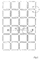
- Figure 1 is a fragmentary plan view of a detector array in accordance with an embodiment of the invention;
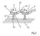
- Figure 2 is a perspective view of the array of Figure 1 shown partly in cross-section taken along lines II-II; and,
- Figures 3 and 4 are cross-sectional side views of the array during different manufacturing steps.
- Referring to Figures 1 and 2, an infrared radiation detector device includes an array of
detector elements 2. Eachelement 2 comprises alayer 4 of pyroelectric material sandwiched between anupper electrode 6 for exposure to the infrared radiation to be detected and alower electrode 8 to form an infrared absorbing structure. Theupper electrodes 6 are formed of a metal or alloy having a high sheet resistance so as to provide the structure with good infrared absorption qualities. For example, the upper electrodes may be formed of an alloy of nickel and chromium (NiCr or nichrome). - Each discrete
lower electrode 8 is connected to an associatedelectronic circuit element 10 located on asubstrate 12, and thus to a signal processing arrangement (not shown). The connection is made via a supportingpillar 14 for thermally insulating theelement 2 from thesubstrate 12. - The
elements 2 are separated along each edge byseparations 16, leaving interconnectingpieces 18 at each corner.Further material 24 having a higher electrical conductivity than the material of theelectrodes 6 is disposed on the edge faces of theelectrodes 6 so as to form a thin conductive rim on adjacent upper electrodes around the periphery of theseparations 16. - Referring to Figures 3 and 4, the
lower electrodes 8 and their electrical connections to thesubstrate 12 viapillars 14 may be formed in the manner described in EP-A-454398, by well-known planar processes. Alayer 4 of pyroelectric material and a layer of NiCr for forming theupper electrodes 6 are deposited on thelower electrodes 8 and covered by alayer 22 of photoresist. The photoresist is patterned in accordance with the required shape of theelements 2, and a NiCr etch is then used to remove the unwanted material. - An electrical contact is made to the
NiCr layer 6, and the assembly is immersed in an electroplating solution. Theelectroplating metal 24, for example gold, is deposited only at the exposed edges of the NiCrlayer 6 because of the masking effect of thepyroelectric layer 4 and thephotoresist 22. - After etching the
pyroelectric layer 4 and removing the remaining photoresist the resulting structure is as shown in Figure 2. Agold rim 24 extends around theseparations 16 between the elements, thus significantly reducing interpixel electrical resistance. - For example, the further material may be disposed around only some of the separations, or may be disposed along only some of the edges of each separation. The further material may be disposed on the upper faces of the interconnected electrodes adjacent the edge rather than on the edge faces, for example by appropriate patterning of the photoresist.
Claims (4)
- An infrared radiation detector device including an array of detector elements comprising an array of interconnected electrodes for exposure to the infrared radiation to be detected, an array of discrete electrodes each connected to signal processing means, and pyroelectric material disposed between the arrays, characterised by further material having a higher electrical conductivity than the interconnected electrodes disposed on and contacting a plurality of the interconnected electrodes at or adjacent at least one edge thereof.
- A device as claimed in claim 1, characterised in that the further material is disposed on and contacting at least one edge face of each of the plurality of interconnected electrodes.
- A device as claimed in claim 1 or 2, characterised in that the further material extends around the peripheries of separations between the plurality of interconnected electrodes.
- A method of manufacturing an infrared radiation detector device as claimed in claim 1, the method comprising:forming an array of discrete electrodes supported on and connected to a substrate for connection to signal processing means;depositing a layer of pyroelectric material thereon; and,depositing a layer of electrode material on the pyroelectric material for forming the interconnected electrodes; the method being characterised by:depositing a layer of photoresist on the electrode material and patterning the photoresist be removing it to expose the electrode material where separations between the interconnected electrodes are required;etching away the exposed electrode material;making an electrical contact to the remaining electrode material and immersing it in an electroplating solution to deposit the further material on the exposed edges of the electrode material; and,removing the remaining photoresist.
Applications Claiming Priority (2)
| Application Number | Priority Date | Filing Date | Title |
|---|---|---|---|
| GB9301147A GB2274543A (en) | 1993-01-21 | 1993-01-21 | Infrared detector |
| GB9301147 | 1993-01-21 |
Publications (2)
| Publication Number | Publication Date |
|---|---|
| EP0608067A1 EP0608067A1 (en) | 1994-07-27 |
| EP0608067B1 true EP0608067B1 (en) | 1996-06-26 |
Family
ID=10729071
Family Applications (1)
| Application Number | Title | Priority Date | Filing Date |
|---|---|---|---|
| EP94300206A Expired - Lifetime EP0608067B1 (en) | 1993-01-21 | 1994-01-12 | Infrared detector |
Country Status (4)
| Country | Link |
|---|---|
| US (1) | US5420420A (en) |
| EP (1) | EP0608067B1 (en) |
| DE (1) | DE69400261T2 (en) |
| GB (1) | GB2274543A (en) |
Families Citing this family (5)
| Publication number | Priority date | Publication date | Assignee | Title |
|---|---|---|---|---|
| TW346688B (en) * | 1996-04-15 | 1998-12-01 | Matsushita Electric Works Ltd | Pyroelectric-type IR receiving element and IR sensor using the same |
| DE19625235A1 (en) * | 1996-06-24 | 1998-01-02 | Abb Patent Gmbh | Motion detector for the detection of moving objects emitting heat radiation |
| US6620731B1 (en) * | 1997-12-18 | 2003-09-16 | Micron Technology, Inc. | Method for fabricating semiconductor components and interconnects with contacts on opposing sides |
| DE102007046451B4 (en) * | 2007-09-28 | 2011-08-25 | Pyreos Ltd. | High resolution thermal radiation detection apparatus, method of making and using the apparatus |
| DE102013204763A1 (en) | 2013-03-19 | 2014-09-25 | Robert Bosch Gmbh | Micromechanical sensor device and corresponding manufacturing method |
Family Cites Families (5)
| Publication number | Priority date | Publication date | Assignee | Title |
|---|---|---|---|---|
| GB2143081B (en) * | 1983-07-06 | 1987-01-14 | Philips Electronic Associated | Infra-red detector with differentially connected pyroelecric elements |
| GB2200246B (en) * | 1985-09-12 | 1989-11-01 | Plessey Co Plc | Thermal detector array |
| GB8812955D0 (en) * | 1988-06-01 | 1988-10-05 | Emi Plc Thorn | Thermal imaging |
| GB8812957D0 (en) * | 1988-06-01 | 1988-10-05 | Thorn Emi Electronics Ltd | Thermal imaging |
| GB9009117D0 (en) * | 1990-04-24 | 1990-08-08 | Emi Plc Thorn | Pyroelectric detector and method of manufacturing the same |
-
1993
- 1993-01-21 GB GB9301147A patent/GB2274543A/en not_active Withdrawn
-
1994
- 1994-01-12 DE DE69400261T patent/DE69400261T2/en not_active Expired - Fee Related
- 1994-01-12 EP EP94300206A patent/EP0608067B1/en not_active Expired - Lifetime
- 1994-01-13 US US08/181,121 patent/US5420420A/en not_active Expired - Fee Related
Also Published As
| Publication number | Publication date |
|---|---|
| DE69400261T2 (en) | 1997-01-30 |
| US5420420A (en) | 1995-05-30 |
| EP0608067A1 (en) | 1994-07-27 |
| GB9301147D0 (en) | 1993-03-10 |
| GB2274543A (en) | 1994-07-27 |
| DE69400261D1 (en) | 1996-08-01 |
Similar Documents
| Publication | Publication Date | Title |
|---|---|---|
| US4663529A (en) | Thermal imaging device and a method of manufacturing a thermal imaging device | |
| US6531951B2 (en) | Force sensor | |
| CA2041127C (en) | Thermal detector device | |
| US5197804A (en) | Resistance temperature sensor | |
| KR890011073A (en) | How to serially connect solar cells on a common substrate | |
| US4385215A (en) | Thin-membrane switch | |
| GB2096820A (en) | Multilayer bus bar | |
| CA1187953A (en) | High capacitance bus bar including multilayer ceramic capacitors | |
| US4725925A (en) | Circuit board | |
| US5420420A (en) | Infrared detector | |
| US4817436A (en) | Measuring device forming fluxmeter and temperature sensor combined and process for preparing the same | |
| EP0375205B1 (en) | Thermal imaging device | |
| CA1181499A (en) | Miniaturized bus bar assembly method | |
| EP0345047B1 (en) | Thermal imaging device | |
| GB2063562A (en) | Thin film sensor | |
| US4942301A (en) | Thermal imaging device | |
| EP0933873A1 (en) | Piezoelectric keyboard | |
| EP0345049B1 (en) | Thermal imaging device | |
| EP0114533A2 (en) | Membrane switch having crossing circuit conductors | |
| JPH01189102A (en) | Manufacture of electrodes of circuit component | |
| GB2200245A (en) | Thermal detector | |
| GB2184606A (en) | Method of producing metallic thin film coil | |
| JP2001066272A (en) | Flow sensor | |
| JPH0610641Y2 (en) | Resistor | |
| JP2002508598A (en) | How to make and assemble photovoltaic cells |
Legal Events
| Date | Code | Title | Description |
|---|---|---|---|
| PUAI | Public reference made under article 153(3) epc to a published international application that has entered the european phase |
Free format text: ORIGINAL CODE: 0009012 |
|
| AK | Designated contracting states |
Kind code of ref document: A1 Designated state(s): DE FR GB SE |
|
| 17P | Request for examination filed |
Effective date: 19950116 |
|
| 17Q | First examination report despatched |
Effective date: 19951017 |
|
| GRAH | Despatch of communication of intention to grant a patent |
Free format text: ORIGINAL CODE: EPIDOS IGRA |
|
| GRAA | (expected) grant |
Free format text: ORIGINAL CODE: 0009210 |
|
| AK | Designated contracting states |
Kind code of ref document: B1 Designated state(s): DE FR GB SE |
|
| REF | Corresponds to: |
Ref document number: 69400261 Country of ref document: DE Date of ref document: 19960801 |
|
| ET | Fr: translation filed | ||
| PLBE | No opposition filed within time limit |
Free format text: ORIGINAL CODE: 0009261 |
|
| STAA | Information on the status of an ep patent application or granted ep patent |
Free format text: STATUS: NO OPPOSITION FILED WITHIN TIME LIMIT |
|
| 26N | No opposition filed | ||
| PGFP | Annual fee paid to national office [announced via postgrant information from national office to epo] |
Ref country code: GB Payment date: 19980402 Year of fee payment: 5 |
|
| PGFP | Annual fee paid to national office [announced via postgrant information from national office to epo] |
Ref country code: SE Payment date: 19980406 Year of fee payment: 5 |
|
| PGFP | Annual fee paid to national office [announced via postgrant information from national office to epo] |
Ref country code: FR Payment date: 19980427 Year of fee payment: 5 |
|
| PGFP | Annual fee paid to national office [announced via postgrant information from national office to epo] |
Ref country code: DE Payment date: 19980428 Year of fee payment: 5 |
|
| PG25 | Lapsed in a contracting state [announced via postgrant information from national office to epo] |
Ref country code: GB Free format text: LAPSE BECAUSE OF NON-PAYMENT OF DUE FEES Effective date: 19990112 |
|
| PG25 | Lapsed in a contracting state [announced via postgrant information from national office to epo] |
Ref country code: SE Free format text: LAPSE BECAUSE OF NON-PAYMENT OF DUE FEES Effective date: 19990113 |
|
| GBPC | Gb: european patent ceased through non-payment of renewal fee |
Effective date: 19990112 |
|
| PG25 | Lapsed in a contracting state [announced via postgrant information from national office to epo] |
Ref country code: FR Free format text: LAPSE BECAUSE OF NON-PAYMENT OF DUE FEES Effective date: 19990930 |
|
| PG25 | Lapsed in a contracting state [announced via postgrant information from national office to epo] |
Ref country code: DE Free format text: LAPSE BECAUSE OF NON-PAYMENT OF DUE FEES Effective date: 19991103 |
|
| REG | Reference to a national code |
Ref country code: FR Ref legal event code: ST |