EP0604170B1 - Integrated circuit configuration for field effect transistors - Google Patents
Integrated circuit configuration for field effect transistors Download PDFInfo
- Publication number
- EP0604170B1 EP0604170B1 EP93310330A EP93310330A EP0604170B1 EP 0604170 B1 EP0604170 B1 EP 0604170B1 EP 93310330 A EP93310330 A EP 93310330A EP 93310330 A EP93310330 A EP 93310330A EP 0604170 B1 EP0604170 B1 EP 0604170B1
- Authority
- EP
- European Patent Office
- Prior art keywords
- fets
- fet
- centroid
- groups
- order
- Prior art date
- Legal status (The legal status is an assumption and is not a legal conclusion. Google has not performed a legal analysis and makes no representation as to the accuracy of the status listed.)
- Expired - Lifetime
Links
Images





Classifications
-
- H—ELECTRICITY
- H10—SEMICONDUCTOR DEVICES; ELECTRIC SOLID-STATE DEVICES NOT OTHERWISE PROVIDED FOR
- H10D—INORGANIC ELECTRIC SEMICONDUCTOR DEVICES
- H10D89/00—Aspects of integrated devices not covered by groups H10D84/00 - H10D88/00
-
- H—ELECTRICITY
- H10—SEMICONDUCTOR DEVICES; ELECTRIC SOLID-STATE DEVICES NOT OTHERWISE PROVIDED FOR
- H10D—INORGANIC ELECTRIC SEMICONDUCTOR DEVICES
- H10D84/00—Integrated devices formed in or on semiconductor substrates that comprise only semiconducting layers, e.g. on Si wafers or on GaAs-on-Si wafers
- H10D84/80—Integrated devices formed in or on semiconductor substrates that comprise only semiconducting layers, e.g. on Si wafers or on GaAs-on-Si wafers characterised by the integration of at least one component covered by groups H10D12/00 or H10D30/00, e.g. integration of IGFETs
- H10D84/82—Integrated devices formed in or on semiconductor substrates that comprise only semiconducting layers, e.g. on Si wafers or on GaAs-on-Si wafers characterised by the integration of at least one component covered by groups H10D12/00 or H10D30/00, e.g. integration of IGFETs of only field-effect components
- H10D84/83—Integrated devices formed in or on semiconductor substrates that comprise only semiconducting layers, e.g. on Si wafers or on GaAs-on-Si wafers characterised by the integration of at least one component covered by groups H10D12/00 or H10D30/00, e.g. integration of IGFETs of only field-effect components of only insulated-gate FETs [IGFET]
-
- Y—GENERAL TAGGING OF NEW TECHNOLOGICAL DEVELOPMENTS; GENERAL TAGGING OF CROSS-SECTIONAL TECHNOLOGIES SPANNING OVER SEVERAL SECTIONS OF THE IPC; TECHNICAL SUBJECTS COVERED BY FORMER USPC CROSS-REFERENCE ART COLLECTIONS [XRACs] AND DIGESTS
- Y10—TECHNICAL SUBJECTS COVERED BY FORMER USPC
- Y10S—TECHNICAL SUBJECTS COVERED BY FORMER USPC CROSS-REFERENCE ART COLLECTIONS [XRACs] AND DIGESTS
- Y10S257/00—Active solid-state devices, e.g. transistors, solid-state diodes
- Y10S257/919—Elements of similar construction connected in series or parallel to average out manufacturing variations in characteristics
Definitions
- This invention relates to integrated circuits.
- MOSFETs Metal Oxide Semiconductor Field-Effect Transistors
- analog Metal Oxide Semiconductor Field-Effect Transistors
- Analog transistors should have long channels with large surface area.
- Digital transistors should have channels as short as possible. However, since a short channel produces a large electric field along the channel's length (ie, between the source and the drain), the channel should be sufficiently long that the electric field does not exceed the breakdown value of the channel material.
- the digital type is used as a switch by applying the proper voltage to the gate of the device, thereby causing a change in resistance of the channel material, thereby either (a) blocking current in the channel (with a high resistance), or (b) allowing it to flow (with a low resistance).
- the high-resistance state requires that the electric field extending between the source and drain remain below the critical value for the channel material.
- the electric field must not be allowed to exceed the critical, breakdown voltage of the material.
- the channel is made as short as possible (for low ON resistance), subject to the requirement that the channel must be long enough to prevent the electric field in the OFF state from exceeding the critical value.
- Analog MOSFETs require different channels: their channels should be long and wide. The channel must be long, in order to obtain high gain. [See, for example, S. M. Sze, Physics of Semiconductor Devices, (1969, John Wiley, ISBN 471 84290 7) chapter 7, section 3, p. 340 et seq].
- the channel must be wide, in order to reduce a particular type of electrical noise, namely, "1/f noise.”
- This type of noise is so-called because it has been experimentally found to be nearly inversely proportional to frequency, as the designation "1/f” indicates. Because of the inverse proportionality, much of the noise power is concentrated at low frequencies. If gain at low frequencies is important, then the "1/f noise" presents a problem.
- this noise is caused by surface traps in the semiconductor material.
- the traps randomly absorb energy and then re-emit the energy as noise.
- One solution to the noise problem is to increase the surface area of the channel, which increases the population of surface traps. This solution reduces the "1/f noise" because, by increasing the number of traps, the number of traps available for absorption is increased, as well as the number available for emission. Restated, in a large population of traps, there is a greater likelihood of finding an available trap to absorb radiated noise.
- the surface area of the channel is made large.
- the length of the channel is made long.
- Analog transistors should have long channels with large surface area.
- Digital transistors should have channels as short as possible (subject to the limit at which breakdown occurs).
- Channel dimensions L (length) and W (Width) are defined in Figure 1.
- the channel length lies between 0.7 and 1.5 microns (a micron equals 10 -6 meter), and the channel width lies between 10 and 50 microns.
- the channel length commonly lies between 16 and 25 microns, and the channel width commonly lies between 40 to 400 microns.
- the channel length is about 10 to 35 times longer, and the channel width ranges from equal to about 40 times wider, than the comparable dimensions in a digital transistor.
- FR-A-2,176,129 discloses a circuit having groups of field effect transistors disposed in accordance with a predetermined patent on the integrated circuit substrate and so as to compensate for variations in electric properties of different regions of the substrate.
- the operational characteristics of such device are disadvantageously limited in view of the manner in which the field effect transistors are formed and connected.
- Patent Abstracts of Japan vol. 8 no.81 relating to JP-A-4,9000953 likewise discloses an arrangement of two MOS transistors on a semiconductor substrate which again seeks to reduce the effect of the difference in the electrical characteristics of the substrate.
- the formation, arrangement and connection of each transistor is disadvantageously limited and serves to limit the operational characteristics of the combined transistor arrangement as a whole.
- an integrated circuit comprising first and second groups of field effect transistor (FET) devices each having first and second electrodes, and a gate electrode, the FET devices being connected such that the first electrodes in both groups are connected together, the gate electrodes in the first group are connected to a first input, the gate electrodes in the second group are connected to a second input, the second electrodes in the first group are connected to a first output and the second electrodes in the second group are connected to a second output, wherein each group of FET devices are spatially located in the integrated circuit such that if the FET devices are regarded as being equal weights, the first and second groups of FET devices have a common centroid and characterized in that each FET device in each group comprises a compound field effect transistor formed from a plurality of field effect transistors having channel lengths of 0.7 to 1.5 microns and connected in series between the first and second electrodes of said at least one FET device
- FIGS 1 and 2 illustrate Field-Effect Transistors (FETs).
- Figures 3A and 3B illustrate a simplified FET amplifier.
- Figure 4 illustrates how FETs can be connected into a differential amplifier.
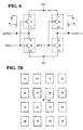
- Figure 5B illustrates how four FETs can be connected into a differential amplifier.
- Figure 5A illustrates the apparatus of Figure 5B, but in simplified form.
- Figure 6 illustrates the apparatus of Figure 5A, but with the layout of the FETs rearranged, for ease of understanding.
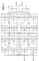
- Figure 7 illustrates how the apparatus of Figure 5B can be cascaded into a larger differential amplifier.
- Figure 7B illustrates two different groups of FETs in the apparatus of Figure 7. One group is shown in solid outline; the other group is shown in phantom outline.
- the FETs in each group form a single compound transistor, or amplifying device.
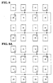
- Figures 8 - 11 illustrate different aspects of the connections of Figure 7.
- Figure 11A illustrates how the apparatus of Figure 5 can be treated as a building block which can be cascaded into a larger amplifier.
- Figure 12 illustrates how the FETs in a cascaded arrangement are arranged around centroids P, P1, and P2.
- Figure 13 illustrates how the centroids are located on diagonals.
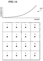
- Figure 14 illustrate a second-order gradient in dopant concentration.
- Figure 15 illustrates four different orientations of the FET array with respect to a substrate having a second-order diffusion gradient.
- FIG. 3A and 3B A simplified FET amplifier is shown in Figures 3A and 3B. The operation can be understood as follows.
- the FET can be constructed so that the channel conductance is almost directly proportional the input voltage (when above threshold).
- the FET acts as an amplifier: the input voltage swing between nine and twelve volts is amplified to a swing between zero and 12 volts.
- Figure 4 shows two of the amplifiers of Figure 3, coupled together as a differential amplifier. They are supplied by a constant current source 25.
- the coupled amplifiers operate as follows:
- Figures 5A and 5B show one approach to connecting digital FETs together, in order to combine the individual channels of the FETs into a larger, composite, channel, which is effectively longer and wider than the individual channels.
- the digital transistors shown are combined into two analog transistors.
- Figure 5A omits the input and output connections shown in Figure 5B.
- the connections to V ss and the load resistors R L are shown at the right side of Figure 5B, and indicate how the four FETs can be connected to form a differential amplifier.
- FETs 1A and 1B are connected in series, but they are not. They are both p-channel devices. Holes are the majority carrier, and the holes flow from source-to-drain, as indicated by the arrows labeled "hole flow.” Consequently, transistors 1A and 1B are actually connected in parallel: their sources are connected together, as are their drains. A similar statement applies to FETs 2A and 2B.
- FIG. 5 The apparatus of Figure 5 can, conceptually, be rearranged to that shown in Figure 6, for ease of understanding.
- the members of each FET pair (1A and 1B) and (2A and 2B) are connected in parallel, providing the effects of a single FET having a wider channel.
- the FETs are positioned as in Figure 5, rather than Figure 6, in order to compensate for diffusion gradients, as will be later discussed.
- the single differential amplifier of Figure 5 can form a building block for constructing a larger amplifier.
- An exemplary differential amplifier containing 16 FETs will be considered.
- the overall connections for the 16-FET amplifier are shown in Figure 7. Since Figure 7 is somewhat complex, it will be considered piecewise.
- Figure 5 contains two differential transistors, namely, that formed by the pair (1A and 1B) and that formed by the pair (2A and 2B).
- the amplifier of Figure 7 is similar in this respect, although, in Figure 7, eight FETs form each differential transistor, not two FETs as in Figure 5.
- One differential transistor is constructed from the eight FETs labeled 1A and 1B.
- the other is constructed from those labeled 2A and 2B.
- Figure 8 shows how the drains of the eight FETs are connected together.
- Figure 8A shows the drain connections for the other eight FETs.
- Figure 9 shows how the sources are connected together.
- Figure 10 shows the gate connections of the eight FETs forming one differential transistor.
- Figure 11 shows the gate connections of the other eight FETs.
- the 16-FET amplifier of Figure 7 can be further cascaded into a larger amplifier. This further cascading can be explained with reference to Figure 11A.
- Figure 11A groups the 16 FETs of Figure 7 into four groups, of four FETs each. Each group is contained within a dashed block. Each dashed block can be viewed as a two-port network, as that term is used in electrical network theory.
- One port includes INPUT 1 and INPUT 2.
- the other port includes OUTPUT 1 and OUTPUT 2.
- INPUTS and OUTPUTS are correspondingly labeled in Figure 5B. (The lead V ss is, strictly speaking, not a member of a port; it is a power supply lead.)
- the cascading of the two-ports is done by connecting them such that
- any feasible number of two-ports can be connected in the preceding manner, into an amplifier containing an arbitrarily large number of FETs.
- the cascaded array of FETs need not be square like the 2 x 2 array of Figure 5 and the 4 x 4 array of Figure 7. That is, the number of rows need not equal the number of columns. However, in all cases, the cascading is done according to the following rules:
- FETs can be symmetrical devices, in the sense that the source can act as the drain. Consequently, the invention can be re-configured such that
- each composite transistor eg, that composed of both 1A and 1B
- the channel width of each composite transistor is effectively about double the width of each individual FET (1A or 1B).
- the increased width also provides additional surface area of the channel, thus reducing 1/f noise, as described hereinabove.
- Each individual transistor in Figure 7 can itself be constructed of several individual transistors (such as 8 to 10 transistors) connected in series.
- the series connection provides a composite transistor having an increased effective channel length.
- FIG. 7B shows a simplified view of the FETs of Figure 7.
- the FETs form two groups:
- Both groups are symmetrical about a centroid P2.
- the centroid can be viewed as a "center of gravity.” That is, the FETs can, conceptually, be viewed as a small equal weights. They are distributed so that the FETs in one group, by themselves with the other group absent, are balanced about the centroid P2. Restated, one could (in theory) balance the circuit on the tip of a needle located at the centroid, with either one or both groups of FETs present.
- Figure 12 shows centroids in a 16 x 16 array. There are three types of centroid: P, P2, and P1. Centroid P is dead-center.
- Centroids P2 lie on the corners of a dashed square. Each P2 is the centroid of a 4 x 4 array, as indicated.
- Each P1 is the centroid of a 2 x 2 array, as indicated.
- Each 2 x 2 array centered about P1 can be termed a "first-order" group, with P1 termed a "first-order" centroid.
- Figure 12 shows sixteen first order groups.
- Each 4 x 4 array centered about P2 can be termed a "second-order" group, with P2 termed a "second-order" centroid.
- Figure 12 shows four second order groups.
- centroid P The 8 x 8 array centered on centroid P can be termed a "third-order group,” with P termed a "third-order” centroid.
- Figure 12 shows one third-order group.
- the cascading can be continued indefinitely.
- the third-order centroid P acts as a centroid for the second-order centroids P2. That is, the centroids P2 themselves have P as a centroid. Further, the second-order centroids P2 act as centroids for the first-order centroids P1.
- the centroids are hierarchical: the centroid P at one order (eg, order 3) act as a centroid for the centroids P2 at the next-lower order (eg order 2), and so on.
- the centroids hierarchical are also cumulative. That is, the third-order centroid P is not only a centroid for the second-order centroids P2, but also for the first-order centroids P1.
- two sets of diagonals can be superimposed on the FET array.
- One set 50 visually connects the FETs providing one output, such as OUTPUT 1.
- the other set 55 visually connects the FETs providing the other output, such as OUTPUT 2.
- the FET array of Figure 7 can be manufactured as an integrated circuit (IC).
- IC integrated circuit
- concentration of dopants introduced into the substrate is not constant at all points: gradients exist.
- One solution, known in the art, is to scatter transistors over several locations on the substrate. The invention provides better compensation than mere scattering, as will now be explained.
- Figure 14 shows a second-order gradient.
- the Figure shows 16 boxes, each representing a position on the substrate. The number in each box indicates the concentration at the center of the box.
- a PLOT indicates the concentration gradient. The concentration changes according to the square of position, and is thus a second-order gradient (in squaring a number, the exponent is "2," corresponding to second order).
- Figure 15A shows the cells of Figure 14, but with one-half of the cells drawn in phantom.
- the phantom cells correspond to FETs 2A or 2B in Figure 7B.
- the solid cells correspond to FETs 1A or 1B.
- the average concentration is the same.
- the average dopant concentration in the channel of one of the differential transistors is 7.5.
- a given square (and thus the FET located in that square) can be identified by its (row, column) address.
- the "1" square is located in (row 1, column 1); a "16" square is located in (row 3, column 4); another "16" square is located in (row 4, column 4).
Landscapes
- Amplifiers (AREA)
Description
- This invention relates to integrated circuits.
- MOSFETs (Metal Oxide Semiconductor Field-Effect Transistors), can be classified into two types, namely, "analog" and "digital." The two types perform different functions. The digital type acts as a switch: it is either ON or OFF. The analog type acts as an amplifier: it amplifies a signal.
- These two types are constructed differently: Analog transistors should have long channels with large surface area. Digital transistors should have channels as short as possible. However, since a short channel produces a large electric field along the channel's length (ie, between the source and the drain), the channel should be sufficiently long that the electric field does not exceed the breakdown value of the channel material. These differences will be explained in more detail.
- The digital type is used as a switch by applying the proper voltage to the gate of the device, thereby causing a change in resistance of the channel material, thereby either (a) blocking current in the channel (with a high resistance), or (b) allowing it to flow (with a low resistance).
- This alternation between high (OFF) and low (ON) resistance presents a design problem. On the one hand, the low-resistance state requires a short channel (ie, the distance between the drain and the source), because
- On the other hand, the high-resistance state requires that the electric field extending between the source and drain remain below the critical value for the channel material.
- For example, as in Figure 2, assume (A) the voltage between the source and drain is five volts, and (B) the source-drain distance L is 1µM (one micro-meter). Consequently, the electric field is 5 volts per 10-6 meter, or 5 x 10⁶ volts per meter. This is a large electric field (in terms of volts per meter), even though the absolute voltage difference between the source and drain is small (ie, five volts).
- The electric field must not be allowed to exceed the critical, breakdown voltage of the material.
- Therefore, in a digital transistor, the channel is made as short as possible (for low ON resistance), subject to the requirement that the channel must be long enough to prevent the electric field in the OFF state from exceeding the critical value.
- Analog MOSFETs require different channels: their channels should be long and wide. The channel must be long, in order to obtain high gain. [See, for example, S. M. Sze, Physics of Semiconductor Devices, (1969, John Wiley, ISBN 471 84290 7) chapter 7, section 3, p. 340 et seq].
- The channel must be wide, in order to reduce a particular type of electrical noise, namely, "1/f noise." This type of noise is so-called because it has been experimentally found to be nearly inversely proportional to frequency, as the designation "1/f" indicates. Because of the inverse proportionality, much of the noise power is concentrated at low frequencies. If gain at low frequencies is important, then the "1/f noise" presents a problem.
- It is theorized that this noise is caused by surface traps in the semiconductor material. The traps randomly absorb energy and then re-emit the energy as noise. One solution to the noise problem is to increase the surface area of the channel, which increases the population of surface traps. This solution reduces the "1/f noise" because, by increasing the number of traps, the number of traps available for absorption is increased, as well as the number available for emission. Restated, in a large population of traps, there is a greater likelihood of finding an available trap to absorb radiated noise.
- Consequently, in an analog transistor, to reduce noise, the surface area of the channel is made large. To increase gain, the length of the channel is made long.
- Therefore, an inherent conflict between digital and analog transistors becomes apparent: Analog transistors should have long channels with large surface area. Digital transistors should have channels as short as possible (subject to the limit at which breakdown occurs).
- Channel dimensions L (length) and W (Width) are defined in Figure 1. In a common digital transistor, the channel length lies between 0.7 and 1.5 microns (a micron equals 10-6 meter), and the channel width lies between 10 and 50 microns. In contrast, for an analog transistor, the channel length commonly lies between 16 and 25 microns, and the channel width commonly lies between 40 to 400 microns. Thus, based on these examples, in an analog transistor, the channel length is about 10 to 35 times longer, and the channel width ranges from equal to about 40 times wider, than the comparable dimensions in a digital transistor.
- FR-A-2,176,129 discloses a circuit having groups of field effect transistors disposed in accordance with a predetermined patent on the integrated circuit substrate and so as to compensate for variations in electric properties of different regions of the substrate. However, the operational characteristics of such device are disadvantageously limited in view of the manner in which the field effect transistors are formed and connected.
- The Patent Abstracts of Japan vol. 8 no.81 relating to JP-A-4,9000953 likewise discloses an arrangement of two MOS transistors on a semiconductor substrate which again seeks to reduce the effect of the difference in the electrical characteristics of the substrate. As with FR-A-2,176,129, the formation, arrangement and connection of each transistor is disadvantageously limited and serves to limit the operational characteristics of the combined transistor arrangement as a whole.
- According to the present invention there is provided an integrated circuit, comprising first and second groups of field effect transistor (FET) devices each having first and second electrodes, and a gate electrode, the FET devices being connected such that the first electrodes in both groups are connected together, the gate electrodes in the first group are connected to a first input, the gate electrodes in the second group are connected to a second input, the second electrodes in the first group are connected to a first output and the second electrodes in the second group are connected to a second output, wherein each group of FET devices are spatially located in the integrated circuit such that if the FET devices are regarded as being equal weights, the first and second groups of FET devices have a common centroid and characterized in that each FET device in each group comprises a compound field effect transistor formed from a plurality of field effect transistors having channel lengths of 0.7 to 1.5 microns and connected in series between the first and second electrodes of said at least one FET device
- Embodiments of the invention will now be described by way of example, with reference to the accompanying drawings, in which:-
- Figures 1 and 2 illustrate Field-Effect Transistors (FETs).
- Figures 3A and 3B illustrate a simplified FET amplifier.
- Figure 4 illustrates how FETs can be connected into a differential amplifier.
- Figure 5B illustrates how four FETs can be connected into a differential amplifier.
- Figure 5A illustrates the apparatus of Figure 5B, but in simplified form.
- Figure 6 illustrates the apparatus of Figure 5A, but with the layout of the FETs rearranged, for ease of understanding.
- Figure 7 illustrates how the apparatus of Figure 5B can be cascaded into a larger differential amplifier.
- Figure 7B illustrates two different groups of FETs in the apparatus of Figure 7. One group is shown in solid outline; the other group is shown in phantom outline. The FETs in each group form a single compound transistor, or amplifying device.
- Figures 8 - 11 illustrate different aspects of the connections of Figure 7.
- Figure 11A illustrates how the apparatus of Figure 5 can be treated as a building block which can be cascaded into a larger amplifier.
- Figure 12 illustrates how the FETs in a cascaded arrangement are arranged around centroids P, P1, and P2.
- Figure 13 illustrates how the centroids are located on diagonals.
- Figure 14 illustrate a second-order gradient in dopant concentration.
- Figure 15 illustrates four different orientations of the FET array with respect to a substrate having a second-order diffusion gradient.
- This description will explain
- (1) the use of an FET as an amplifier,
- (2) the use of two FETs as a differential amplifier, and
- (3) the construction of analog FETs from digital FETs, and the configuration of the analog FETs as a differential amplifier.
-
- Then, this discussion will explain important features, some of which result from the construction of point (3), above.
- A simplified FET amplifier is shown in Figures 3A and 3B. The operation can be understood as follows.
- In Figure 3A, assume that Vss equals 12 volts. If the INPUT is pulled HIGH, say to 12 volts, p-
channel FET 20 is turned OFF. In the OFF state, this FET, in effect, becomes a large resistor R, as shown in Figure 3B. Because R and the load resistor RL act as a voltage divider, and because R is significantly greater than RL, the OUTPUT voltage is driven to nearly ZERO. - Conversely, if the INPUT is LOW, say at nine volts, R becomes a very low resistance, and the OUTPUT voltage almost reaches Vss, or 12 volts.
- For intermediate INPUT voltages between HIGH and LOW, the FET can be constructed so that the channel conductance is almost directly proportional the input voltage (when above threshold). Thus, the FET acts as an amplifier: the input voltage swing between nine and twelve volts is amplified to a swing between zero and 12 volts.
- Figure 4 shows two of the amplifiers of Figure 3, coupled together as a differential amplifier. They are supplied by a constant
current source 25. The coupled amplifiers operate as follows: - If both
INPUT 1 andINPUT 2 are HIGH, both FETs go OFF. Now, OUTPUT_1 and OUTPUT_2 are at equal voltages, at about ZERO volts. Because the OUTPUT voltages are equal, the difference between them is zero. - If both INPUTS are LOW, both FETs go ON, both OUTPUTS go to near 12 volts, and, again, the difference between the OUTPUT voltages is zero.
- If
INPUT 1 is at a higher voltage than INPUT 2 (ie, there is a difference signal present), the resistance ofFET 27 will be higher than that ofFET 29. Consequently,OUTPUT 2 will exceedOUTPUT 1 in voltage. Now, unlike the previous two cases, there is a difference in OUTPUT voltages. - These three situations illustrates, in simplified form, how the apparatus of Figure 4 operates as a differential amplifier: it provides a differential OUTPUT voltage in response to a differential INPUT voltage input.
- Figures 5A and 5B show one approach to connecting digital FETs together, in order to combine the individual channels of the FETs into a larger, composite, channel, which is effectively longer and wider than the individual channels. The digital transistors shown are combined into two analog transistors. For clarity, Figure 5A omits the input and output connections shown in Figure 5B. The connections to Vss and the load resistors RL are shown at the right side of Figure 5B, and indicate how the four FETs can be connected to form a differential amplifier.
- It may appear that
FETs FETs transistors FETs - The apparatus of Figure 5 can, conceptually, be rearranged to that shown in Figure 6, for ease of understanding. The members of each FET pair (1A and 1B) and (2A and 2B) are connected in parallel, providing the effects of a single FET having a wider channel. However, the FETs are positioned as in Figure 5, rather than Figure 6, in order to compensate for diffusion gradients, as will be later discussed.
- For ease of illustration, the current sources of Figure 5B have been omitted in the subsequent Figures.
- The single differential amplifier of Figure 5 can form a building block for constructing a larger amplifier. An exemplary differential amplifier containing 16 FETs will be considered. The overall connections for the 16-FET amplifier are shown in Figure 7. Since Figure 7 is somewhat complex, it will be considered piecewise.
- Recall that Figure 5 contains two differential transistors, namely, that formed by the pair (1A and 1B) and that formed by the pair (2A and 2B). The amplifier of Figure 7 is similar in this respect, although, in Figure 7, eight FETs form each differential transistor, not two FETs as in Figure 5. One differential transistor is constructed from the eight FETs labeled 1A and 1B. The other is constructed from those labeled 2A and 2B.
- For the amplifier of Figure 7, Figure 8 shows how the drains of the eight FETs are connected together. Figure 8A shows the drain connections for the other eight FETs.
- Figure 9 shows how the sources are connected together.
- Figure 10 shows the gate connections of the eight FETs forming one differential transistor.
- Figure 11 shows the gate connections of the other eight FETs.
- As in Figure 5, in Figure 7, Vss and two load resistors RL are connected, showing one way to use the apparatus of Figure 7 as a differential amplifier.
- The 16-FET amplifier of Figure 7 can be further cascaded into a larger amplifier. This further cascading can be explained with reference to Figure 11A. Figure 11A groups the 16 FETs of Figure 7 into four groups, of four FETs each. Each group is contained within a dashed block. Each dashed block can be viewed as a two-port network, as that term is used in electrical network theory.
- One port includes
INPUT 1 andINPUT 2. The other port includesOUTPUT 1 andOUTPUT 2. These INPUTS and OUTPUTS are correspondingly labeled in Figure 5B. (The lead Vss is, strictly speaking, not a member of a port; it is a power supply lead.) - The cascading of the two-ports is done by connecting them such that
- 1. All INPUT_1's are connected in common.
- 2. All INPUT_2's are connected in common.
- 3. All
OUTPUT 1's are connected in common. - 4. All OUTPUT_2's are connected in common. Figure 7 illustrates these connections for a 16-FET system.
-
- More generally, any feasible number of two-ports can be connected in the preceding manner, into an amplifier containing an arbitrarily large number of FETs.
- The cascaded array of FETs need not be square like the 2 x 2 array of Figure 5 and the 4 x 4 array of Figure 7. That is, the number of rows need not equal the number of columns. However, in all cases, the cascading is done according to the following rules:
- 1) The sources are connected in common.
- 2) Half of the gates are connected to one differential input; the other half are connected to the other differential input.
- 3) Half of the drains are connected to one differential output; the other half are connected to the other differential output.
-
- It is recognized that FETs can be symmetrical devices, in the sense that the source can act as the drain. Consequently, the invention can be re-configured such that
- all S's, such as those in Figure 5, are replaced by D's,
- all D's replaced by S's,
- Vss is replaced by ground, and
- the ground symbols are replaced by Vdd.
- The cascading just described, in effect, provides a composite (or compound) transistor having a wider channel than the individual FETs. For example, in Figure 6, the channel width of each composite transistor (eg, that composed of both 1A and 1B) is effectively about double the width of each individual FET (1A or 1B).
- The increased width also provides additional surface area of the channel, thus reducing 1/f noise, as described hereinabove.
- Each individual transistor in Figure 7 (such as 1A) can itself be constructed of several individual transistors (such as 8 to 10 transistors) connected in series. The series connection provides a composite transistor having an increased effective channel length.
- Figure 7B shows a simplified view of the FETs of Figure 7. In Figure 7B, the FETs form two groups:
- (1) those connecting to OUTPUT 2 (shown in dashed outline) and
- (2) those connecting to OUTPUT 1 (shown in solid outline).
-
- Both groups are symmetrical about a centroid P2. The centroid can be viewed as a "center of gravity." That is, the FETs can, conceptually, be viewed as a small equal weights. They are distributed so that the FETs in one group, by themselves with the other group absent, are balanced about the centroid P2. Restated, one could (in theory) balance the circuit on the tip of a needle located at the centroid, with either one or both groups of FETs present.
- Figure 12 shows centroids in a 16 x 16 array. There are three types of centroid: P, P2, and P1. Centroid P is dead-center.
- Centroids P2 lie on the corners of a dashed square. Each P2 is the centroid of a 4 x 4 array, as indicated.
- Each P1 is the centroid of a 2 x 2 array, as indicated.
- Each 2 x 2 array centered about P1 can be termed a "first-order" group, with P1 termed a "first-order" centroid. Figure 12 shows sixteen first order groups.
- Each 4 x 4 array centered about P2 can be termed a "second-order" group, with P2 termed a "second-order" centroid. Figure 12 shows four second order groups.
- The 8 x 8 array centered on centroid P can be termed a "third-order group," with P termed a "third-order" centroid. Figure 12 shows one third-order group.
- In the case of a larger, 16 x 16 array (not shown), there would be 64 first-order groups, 16 second-order groups, 4 third-order groups, and a new designation, namely, a fourth-order group.
- In principle, the cascading can be continued indefinitely.
- It is significant that, in Figure 12, the third-order centroid P acts as a centroid for the second-order centroids P2. That is, the centroids P2 themselves have P as a centroid. Further, the second-order centroids P2 act as centroids for the first-order centroids P1. Thus, the centroids are hierarchical: the centroid P at one order (eg, order 3) act as a centroid for the centroids P2 at the next-lower order (eg order 2), and so on.
- Not only are the centroids hierarchical, but they are also cumulative. That is, the third-order centroid P is not only a centroid for the second-order centroids P2, but also for the first-order centroids P1.
- As shown in Figure 13, two sets of diagonals can be superimposed on the FET array. One set 50 visually connects the FETs providing one output, such as
OUTPUT 1. Theother set 55 visually connects the FETs providing the other output, such asOUTPUT 2. - The sets of diagonals intersect (when superimposed), and if the array is a square, the diagonals will intersect at right angles.
- The diagonals intersect the centroids, as indicated (only a few centroids are shown to avoid clutter).
- The FET array of Figure 7 can be manufactured as an integrated circuit (IC). In IC's generally, the concentration of dopants introduced into the substrate is not constant at all points: gradients exist. One solution, known in the art, is to scatter transistors over several locations on the substrate. The invention provides better compensation than mere scattering, as will now be explained.
- Figure 14 shows a second-order gradient. The Figure shows 16 boxes, each representing a position on the substrate. The number in each box indicates the concentration at the center of the box. A PLOT indicates the concentration gradient. The concentration changes according to the square of position, and is thus a second-order gradient (in squaring a number, the exponent is "2," corresponding to second order).
- Figure 15A shows the cells of Figure 14, but with one-half of the cells drawn in phantom. The phantom cells correspond to
FETs FETs - The average concentration for the phantom cells is
- Thus, with this configuration, the average dopant concentration in the channel of one of the differential transistors is 7.5.
- In addition, this average concentration does not change if the cells are re-oriented with respect to the concentration gradient. Figures 15B - 15D illustrate this lack of change.
- It can be shown that these average concentrations in the differential transistors are closer (in Figure 15 they are identical) than if the two differential transistors were constructed from transistors selected at random in Figure 15.
- In Figure 15, a given square (and thus the FET located in that square) can be identified by its (row, column) address. For example, the "1" square is located in (
row 1, column 1); a "16" square is located in (row 3, column 4); another "16" square is located in (row 4, column 4). - These locations are either "odd" or "even," based on the sum of (row-plus-column). For example, the "1" square is at an even location: 1 + 1 = 2, and 2 is an even number.
- Thus, there has been described an integrated circuit which:
- provides an array of FETs;
- divides the array into two groups of FETs (such as the phantom and solid cells in Figure 15);
- connects the FETs of each group into a composite differential transistor (or amplifier); and
- as a result, the composite transistors become comparable in average channel concentration, irrespective of the orientation of the array with respect to the gradient Figure 15.
Claims (2)
- An integrated circuit, comprising first (1A, 1B) and second (2A, 2B) groups of field effect transistor (FET) devices each having first (S) and second (D) electrodes, and a gate electrode (G), the FET devices (1A, 1B, 2A, 2B) being connected such that the first electrodes (S) in both groups are connected together, the gate electrodes (G) in the first group (1A, 1B) are connected to a first input, the gate electrodes (G) in the second group (2A, 2B) are connected to a second input, the second electrodes (D) in the first group (1A, 1B) are connected to a first output and the second electrodes (D) in the second group (2A, 2B) are connected to a second output, wherein each group of FET devices (1A, 1B, 2A, 2B) are spatially located in the integrated circuit such that if the FET devices (1A, 1B, 2A, 2B) are regarded as being equal weights, the first and second groups of FET devices have a common centroid and characterized in that each FET device (1A,1B,2A,2B) in each group comprises a compound field effect transistor formed from a plurality of field effect transistors having channel lengths of 0.7 to 1.5 microns and connected in series between the first (S) and second (D) electrodes of said at least one FET device .
- An integrated circuit according to Claim 1, characterized in that the centroid of each first and second group of FET devices is a first order centroid (P1), the circuit comprising a first plurality of said first and second groups and a second plurality of said first and second groups, wherein a centroid of the first order centroids of the said first plurality of groups is a second order centroid (P2) which is itself lennar to a centroid of the first order centroids (P1) of the said second plurality of groups.
Applications Claiming Priority (2)
| Application Number | Priority Date | Filing Date | Title |
|---|---|---|---|
| US99653492A | 1992-12-24 | 1992-12-24 | |
| US996534 | 1992-12-24 |
Publications (2)
| Publication Number | Publication Date |
|---|---|
| EP0604170A1 EP0604170A1 (en) | 1994-06-29 |
| EP0604170B1 true EP0604170B1 (en) | 2001-08-16 |
Family
ID=25543020
Family Applications (1)
| Application Number | Title | Priority Date | Filing Date |
|---|---|---|---|
| EP93310330A Expired - Lifetime EP0604170B1 (en) | 1992-12-24 | 1993-12-20 | Integrated circuit configuration for field effect transistors |
Country Status (4)
| Country | Link |
|---|---|
| US (1) | US5488249A (en) |
| EP (1) | EP0604170B1 (en) |
| JP (1) | JP3516307B2 (en) |
| DE (1) | DE69330594T2 (en) |
Families Citing this family (5)
| Publication number | Priority date | Publication date | Assignee | Title |
|---|---|---|---|---|
| US6316809B1 (en) * | 1999-01-06 | 2001-11-13 | Lucent Technologies Inc. | Analog MOSFET devices |
| KR100605500B1 (en) * | 2005-03-03 | 2006-07-28 | 삼성전자주식회사 | Semiconductor devices having a line type active region and manufacturing methods thereof |
| US7872502B2 (en) * | 2006-07-12 | 2011-01-18 | Hewlett-Packard Development Company, L.P. | Defect-and-failure-tolerant demultiplexer using series replication and error-control encoding |
| DE102008021564B4 (en) * | 2008-04-30 | 2016-01-28 | Globalfoundries Inc. | Integrated circuit with multiple circuit elements with less mismatch |
| CN110411483B (en) * | 2019-08-26 | 2021-08-17 | 中南大学 | Readout circuit and sensor array of a novel large-scale sensor array |
Citations (1)
| Publication number | Priority date | Publication date | Assignee | Title |
|---|---|---|---|---|
| EP0403174A2 (en) * | 1989-06-12 | 1990-12-19 | Oki Electric Industry Co., Ltd. | Differential amplifying circuit operable at high speed |
Family Cites Families (12)
| Publication number | Priority date | Publication date | Assignee | Title |
|---|---|---|---|---|
| US3477031A (en) * | 1966-09-09 | 1969-11-04 | Hitachi Ltd | Differential amplifier circuit employing multiple differential amplifier stages |
| JPS53675B2 (en) * | 1972-03-16 | 1978-01-11 | ||
| JPS5437668A (en) * | 1977-08-31 | 1979-03-20 | Sansui Electric Co | Differential amplifier |
| JPS59953A (en) * | 1982-06-26 | 1984-01-06 | Toshiba Corp | Mos type semiconductor integrated circuit |
| JPS61292358A (en) * | 1985-06-19 | 1986-12-23 | Fujitsu Ltd | Manufacture of mis field effect transistor |
| US5257095A (en) * | 1985-12-04 | 1993-10-26 | Advanced Micro Devices, Inc. | Common geometry high voltage tolerant long channel and high speed short channel field effect transistors |
| US4907201A (en) * | 1986-05-07 | 1990-03-06 | Mitsubishi Denki Kabushiki Kaisha | MOS transistor circuit |
| US4884118A (en) * | 1986-05-19 | 1989-11-28 | Lsi Logic Corporation | Double metal HCMOS compacted array |
| US4884115A (en) * | 1987-02-27 | 1989-11-28 | Siemens Aktiengesellschaft | Basic cell for a gate array arrangement in CMOS Technology |
| US4851892A (en) * | 1987-09-08 | 1989-07-25 | Motorola, Inc. | Standard cell array having fake gate for isolating devices from supply voltages |
| US4871978A (en) * | 1988-08-10 | 1989-10-03 | Actel Corporation | High-speed static differential sense amplifier |
| JPH0814995B2 (en) * | 1989-01-27 | 1996-02-14 | 株式会社東芝 | Semiconductor memory |
-
1993
- 1993-12-07 JP JP33988693A patent/JP3516307B2/en not_active Expired - Lifetime
- 1993-12-20 EP EP93310330A patent/EP0604170B1/en not_active Expired - Lifetime
- 1993-12-20 DE DE69330594T patent/DE69330594T2/en not_active Expired - Lifetime
-
1994
- 1994-05-06 US US08/239,166 patent/US5488249A/en not_active Expired - Lifetime
Patent Citations (1)
| Publication number | Priority date | Publication date | Assignee | Title |
|---|---|---|---|---|
| EP0403174A2 (en) * | 1989-06-12 | 1990-12-19 | Oki Electric Industry Co., Ltd. | Differential amplifying circuit operable at high speed |
Non-Patent Citations (1)
| Title |
|---|
| Semiconductor Devices, Physics & Technology S.M.Sze, pub. 1985 John Wiley, pgs. 213-219 * |
Also Published As
| Publication number | Publication date |
|---|---|
| EP0604170A1 (en) | 1994-06-29 |
| DE69330594D1 (en) | 2001-09-20 |
| US5488249A (en) | 1996-01-30 |
| DE69330594T2 (en) | 2002-04-18 |
| JPH06237129A (en) | 1994-08-23 |
| JP3516307B2 (en) | 2004-04-05 |
Similar Documents
| Publication | Publication Date | Title |
|---|---|---|
| US4518926A (en) | Gate-coupled field-effect transistor pair amplifier | |
| US5006816A (en) | Semiconductor integrated circuit including differential transistor circuit having a pair of FETs | |
| US3477031A (en) | Differential amplifier circuit employing multiple differential amplifier stages | |
| KR20060049488A (en) | High frequency switching circuit and semiconductor device using same | |
| US3956643A (en) | MOS analog multiplier | |
| US5610429A (en) | Differential analog transistors constructed from digital transistors | |
| JP3325396B2 (en) | Semiconductor integrated circuit | |
| US5488249A (en) | Differential analog transistors constructed from digital transistors | |
| EP0361546B1 (en) | Semiconductor memory device | |
| KR100277387B1 (en) | Linear voltage control resistor | |
| GB2335076A (en) | Electrostatic discharge protection in semiconductor devices | |
| KR900008753B1 (en) | Differential amplifier | |
| US6414536B1 (en) | Electrically adjustable CMOS integrated voltage reference circuit | |
| US5541548A (en) | Analog output driver for gate arrays | |
| US3882409A (en) | Differential amplifier circuit | |
| US4316103A (en) | Circuit for coupling signals from a sensor | |
| US3675143A (en) | All-fet linear voltage amplifier | |
| JPH0571145B2 (en) | ||
| EP0528659B1 (en) | Impedance multiplier | |
| KR100203965B1 (en) | Semiconductor integrated circuit | |
| US3359503A (en) | High gain amplifier employing cascaded opposite conductivity field effect transistors | |
| US20050024150A1 (en) | Monolithic amplifier with high-value, monolithically formed passive feedback resistor | |
| RU2069448C1 (en) | Amplifier | |
| EP2824534A2 (en) | Bulk-modulated current source | |
| EP0404360B1 (en) | Shielded transistor device |
Legal Events
| Date | Code | Title | Description |
|---|---|---|---|
| PUAI | Public reference made under article 153(3) epc to a published international application that has entered the european phase |
Free format text: ORIGINAL CODE: 0009012 |
|
| AK | Designated contracting states |
Kind code of ref document: A1 Designated state(s): DE GB |
|
| RAP1 | Party data changed (applicant data changed or rights of an application transferred) |
Owner name: AT&T GLOBAL INFORMATION SOLUTIONS INTERNATIONAL IN |
|
| 17P | Request for examination filed |
Effective date: 19941220 |
|
| RAP1 | Party data changed (applicant data changed or rights of an application transferred) |
Owner name: HYUNDAI ELECTRONICS AMERICA Owner name: AT&T GLOBAL INFORMATION SOLUTIONS INTERNATIONAL IN |
|
| RAP1 | Party data changed (applicant data changed or rights of an application transferred) |
Owner name: SYMBIOS LOGIC INC. Owner name: HYUNDAI ELECTRONICS AMERICA Owner name: AT&T GLOBAL INFORMATION SOLUTIONS INTERNATIONAL IN |
|
| 17Q | First examination report despatched |
Effective date: 19960809 |
|
| RAP1 | Party data changed (applicant data changed or rights of an application transferred) |
Owner name: SYMBIOS LOGIC INC. Owner name: HYUNDAI ELECTRONICS AMERICA Owner name: NCR INTERNATIONAL, INC. |
|
| RAP1 | Party data changed (applicant data changed or rights of an application transferred) |
Owner name: SYMBIOS, INC. Owner name: HYUNDAI ELECTRONICS AMERICA Owner name: NCR INTERNATIONAL, INC. |
|
| GRAG | Despatch of communication of intention to grant |
Free format text: ORIGINAL CODE: EPIDOS AGRA |
|
| GRAG | Despatch of communication of intention to grant |
Free format text: ORIGINAL CODE: EPIDOS AGRA |
|
| GRAH | Despatch of communication of intention to grant a patent |
Free format text: ORIGINAL CODE: EPIDOS IGRA |
|
| GRAH | Despatch of communication of intention to grant a patent |
Free format text: ORIGINAL CODE: EPIDOS IGRA |
|
| GRAA | (expected) grant |
Free format text: ORIGINAL CODE: 0009210 |
|
| AK | Designated contracting states |
Kind code of ref document: B1 Designated state(s): DE GB |
|
| REF | Corresponds to: |
Ref document number: 69330594 Country of ref document: DE Date of ref document: 20010920 |
|
| REG | Reference to a national code |
Ref country code: GB Ref legal event code: IF02 |
|
| PLBE | No opposition filed within time limit |
Free format text: ORIGINAL CODE: 0009261 |
|
| STAA | Information on the status of an ep patent application or granted ep patent |
Free format text: STATUS: NO OPPOSITION FILED WITHIN TIME LIMIT |
|
| 26N | No opposition filed | ||
| REG | Reference to a national code |
Ref country code: GB Ref legal event code: 732E |
|
| REG | Reference to a national code |
Ref country code: GB Ref legal event code: 732E |
|
| REG | Reference to a national code |
Ref country code: GB Ref legal event code: 732E |
|
| PGFP | Annual fee paid to national office [announced via postgrant information from national office to epo] |
Ref country code: GB Payment date: 20121227 Year of fee payment: 20 |
|
| PGFP | Annual fee paid to national office [announced via postgrant information from national office to epo] |
Ref country code: DE Payment date: 20121231 Year of fee payment: 20 |
|
| REG | Reference to a national code |
Ref country code: DE Ref legal event code: R071 Ref document number: 69330594 Country of ref document: DE |
|
| REG | Reference to a national code |
Ref country code: DE Ref legal event code: R071 Ref document number: 69330594 Country of ref document: DE |
|
| REG | Reference to a national code |
Ref country code: GB Ref legal event code: PE20 Expiry date: 20131219 |
|
| PG25 | Lapsed in a contracting state [announced via postgrant information from national office to epo] |
Ref country code: DE Free format text: LAPSE BECAUSE OF EXPIRATION OF PROTECTION Effective date: 20131221 Ref country code: GB Free format text: LAPSE BECAUSE OF EXPIRATION OF PROTECTION Effective date: 20131219 |