EP0603737A2 - Hybrid bipolar/field-effect power transistor in group III-V material system - Google Patents
Hybrid bipolar/field-effect power transistor in group III-V material system Download PDFInfo
- Publication number
- EP0603737A2 EP0603737A2 EP93120248A EP93120248A EP0603737A2 EP 0603737 A2 EP0603737 A2 EP 0603737A2 EP 93120248 A EP93120248 A EP 93120248A EP 93120248 A EP93120248 A EP 93120248A EP 0603737 A2 EP0603737 A2 EP 0603737A2
- Authority
- EP
- European Patent Office
- Prior art keywords
- layer
- transistor
- channel
- hybrid
- hybrid transistor
- Prior art date
- Legal status (The legal status is an assumption and is not a legal conclusion. Google has not performed a legal analysis and makes no representation as to the accuracy of the status listed.)
- Withdrawn
Links
- 239000000463 material Substances 0.000 title claims abstract description 37
- 230000005669 field effect Effects 0.000 title claims abstract description 25
- 108091006146 Channels Proteins 0.000 claims abstract description 60
- 238000002347 injection Methods 0.000 claims abstract description 31
- 239000007924 injection Substances 0.000 claims abstract description 31
- 102000004129 N-Type Calcium Channels Human genes 0.000 claims abstract description 6
- 108090000699 N-Type Calcium Channels Proteins 0.000 claims abstract description 6
- XUIMIQQOPSSXEZ-UHFFFAOYSA-N Silicon Chemical compound [Si] XUIMIQQOPSSXEZ-UHFFFAOYSA-N 0.000 claims description 15
- 229910052710 silicon Inorganic materials 0.000 claims description 15
- 239000010703 silicon Substances 0.000 claims description 15
- 150000002500 ions Chemical class 0.000 claims description 14
- 229910052751 metal Inorganic materials 0.000 claims description 10
- 239000002184 metal Substances 0.000 claims description 10
- 239000004065 semiconductor Substances 0.000 claims description 7
- JBRZTFJDHDCESZ-UHFFFAOYSA-N AsGa Chemical compound [As]#[Ga] JBRZTFJDHDCESZ-UHFFFAOYSA-N 0.000 claims description 6
- 229910000530 Gallium indium arsenide Inorganic materials 0.000 claims description 6
- FTWRSWRBSVXQPI-UHFFFAOYSA-N alumanylidynearsane;gallanylidynearsane Chemical compound [As]#[Al].[As]#[Ga] FTWRSWRBSVXQPI-UHFFFAOYSA-N 0.000 claims description 6
- GPXJNWSHGFTCBW-UHFFFAOYSA-N Indium phosphide Chemical compound [In]#P GPXJNWSHGFTCBW-UHFFFAOYSA-N 0.000 claims description 5
- 229910052790 beryllium Inorganic materials 0.000 claims description 5
- ATBAMAFKBVZNFJ-UHFFFAOYSA-N beryllium atom Chemical compound [Be] ATBAMAFKBVZNFJ-UHFFFAOYSA-N 0.000 claims description 5
- 239000011669 selenium Substances 0.000 claims description 4
- 230000004888 barrier function Effects 0.000 claims description 3
- 229910000673 Indium arsenide Inorganic materials 0.000 claims description 2
- BUGBHKTXTAQXES-UHFFFAOYSA-N Selenium Chemical compound [Se] BUGBHKTXTAQXES-UHFFFAOYSA-N 0.000 claims description 2
- ATJFFYVFTNAWJD-UHFFFAOYSA-N Tin Chemical compound [Sn] ATJFFYVFTNAWJD-UHFFFAOYSA-N 0.000 claims description 2
- AJGDITRVXRPLBY-UHFFFAOYSA-N aluminum indium Chemical compound [Al].[In] AJGDITRVXRPLBY-UHFFFAOYSA-N 0.000 claims description 2
- 239000002800 charge carrier Substances 0.000 claims description 2
- 229910052711 selenium Inorganic materials 0.000 claims description 2
- JBQYATWDVHIOAR-UHFFFAOYSA-N tellanylidenegermanium Chemical compound [Te]=[Ge] JBQYATWDVHIOAR-UHFFFAOYSA-N 0.000 claims description 2
- 238000004519 manufacturing process Methods 0.000 abstract description 3
- 230000008901 benefit Effects 0.000 description 4
- 230000015556 catabolic process Effects 0.000 description 4
- 230000009977 dual effect Effects 0.000 description 4
- 239000012212 insulator Substances 0.000 description 4
- 230000003071 parasitic effect Effects 0.000 description 3
- VYPSYNLAJGMNEJ-UHFFFAOYSA-N Silicium dioxide Chemical compound O=[Si]=O VYPSYNLAJGMNEJ-UHFFFAOYSA-N 0.000 description 2
- HCHKCACWOHOZIP-UHFFFAOYSA-N Zinc Chemical compound [Zn] HCHKCACWOHOZIP-UHFFFAOYSA-N 0.000 description 2
- 238000000151 deposition Methods 0.000 description 2
- 230000008021 deposition Effects 0.000 description 2
- 238000001465 metallisation Methods 0.000 description 2
- BASFCYQUMIYNBI-UHFFFAOYSA-N platinum Chemical compound [Pt] BASFCYQUMIYNBI-UHFFFAOYSA-N 0.000 description 2
- 239000011701 zinc Substances 0.000 description 2
- 229910052725 zinc Inorganic materials 0.000 description 2
- 229910001218 Gallium arsenide Inorganic materials 0.000 description 1
- 239000004952 Polyamide Substances 0.000 description 1
- 229910052581 Si3N4 Inorganic materials 0.000 description 1
- RTAQQCXQSZGOHL-UHFFFAOYSA-N Titanium Chemical compound [Ti] RTAQQCXQSZGOHL-UHFFFAOYSA-N 0.000 description 1
- 230000009471 action Effects 0.000 description 1
- 230000005684 electric field Effects 0.000 description 1
- 238000005516 engineering process Methods 0.000 description 1
- PCHJSUWPFVWCPO-UHFFFAOYSA-N gold Chemical compound [Au] PCHJSUWPFVWCPO-UHFFFAOYSA-N 0.000 description 1
- 229910052737 gold Inorganic materials 0.000 description 1
- 239000010931 gold Substances 0.000 description 1
- 239000012535 impurity Substances 0.000 description 1
- 239000011810 insulating material Substances 0.000 description 1
- 238000005468 ion implantation Methods 0.000 description 1
- 238000012986 modification Methods 0.000 description 1
- 230000004048 modification Effects 0.000 description 1
- 239000013642 negative control Substances 0.000 description 1
- 238000000059 patterning Methods 0.000 description 1
- 229910052697 platinum Inorganic materials 0.000 description 1
- 229920002647 polyamide Polymers 0.000 description 1
- 239000003870 refractory metal Substances 0.000 description 1
- 235000012239 silicon dioxide Nutrition 0.000 description 1
- 239000000377 silicon dioxide Substances 0.000 description 1
- HQVNEWCFYHHQES-UHFFFAOYSA-N silicon nitride Chemical compound N12[Si]34N5[Si]62N3[Si]51N64 HQVNEWCFYHHQES-UHFFFAOYSA-N 0.000 description 1
- 239000010936 titanium Substances 0.000 description 1
- 229910052719 titanium Inorganic materials 0.000 description 1
- 230000005533 two-dimensional electron gas Effects 0.000 description 1
Images


Classifications
-
- H—ELECTRICITY
- H01—ELECTRIC ELEMENTS
- H01L—SEMICONDUCTOR DEVICES NOT COVERED BY CLASS H10
- H01L29/00—Semiconductor devices adapted for rectifying, amplifying, oscillating or switching, or capacitors or resistors with at least one potential-jump barrier or surface barrier, e.g. PN junction depletion layer or carrier concentration layer; Details of semiconductor bodies or of electrodes thereof ; Multistep manufacturing processes therefor
- H01L29/66—Types of semiconductor device ; Multistep manufacturing processes therefor
- H01L29/68—Types of semiconductor device ; Multistep manufacturing processes therefor controllable by only the electric current supplied, or only the electric potential applied, to an electrode which does not carry the current to be rectified, amplified or switched
- H01L29/70—Bipolar devices
- H01L29/72—Transistor-type devices, i.e. able to continuously respond to applied control signals
- H01L29/739—Transistor-type devices, i.e. able to continuously respond to applied control signals controlled by field-effect, e.g. bipolar static induction transistors [BSIT]
- H01L29/7391—Gated diode structures
- H01L29/7392—Gated diode structures with PN junction gate, e.g. field controlled thyristors (FCTh), static induction thyristors (SITh)
-
- H—ELECTRICITY
- H01—ELECTRIC ELEMENTS
- H01L—SEMICONDUCTOR DEVICES NOT COVERED BY CLASS H10
- H01L27/00—Devices consisting of a plurality of semiconductor or other solid-state components formed in or on a common substrate
- H01L27/02—Devices consisting of a plurality of semiconductor or other solid-state components formed in or on a common substrate including semiconductor components specially adapted for rectifying, oscillating, amplifying or switching and having at least one potential-jump barrier or surface barrier; including integrated passive circuit elements with at least one potential-jump barrier or surface barrier
- H01L27/04—Devices consisting of a plurality of semiconductor or other solid-state components formed in or on a common substrate including semiconductor components specially adapted for rectifying, oscillating, amplifying or switching and having at least one potential-jump barrier or surface barrier; including integrated passive circuit elements with at least one potential-jump barrier or surface barrier the substrate being a semiconductor body
- H01L27/06—Devices consisting of a plurality of semiconductor or other solid-state components formed in or on a common substrate including semiconductor components specially adapted for rectifying, oscillating, amplifying or switching and having at least one potential-jump barrier or surface barrier; including integrated passive circuit elements with at least one potential-jump barrier or surface barrier the substrate being a semiconductor body including a plurality of individual components in a non-repetitive configuration
-
- H—ELECTRICITY
- H01—ELECTRIC ELEMENTS
- H01L—SEMICONDUCTOR DEVICES NOT COVERED BY CLASS H10
- H01L29/00—Semiconductor devices adapted for rectifying, amplifying, oscillating or switching, or capacitors or resistors with at least one potential-jump barrier or surface barrier, e.g. PN junction depletion layer or carrier concentration layer; Details of semiconductor bodies or of electrodes thereof ; Multistep manufacturing processes therefor
- H01L29/66—Types of semiconductor device ; Multistep manufacturing processes therefor
- H01L29/68—Types of semiconductor device ; Multistep manufacturing processes therefor controllable by only the electric current supplied, or only the electric potential applied, to an electrode which does not carry the current to be rectified, amplified or switched
- H01L29/70—Bipolar devices
- H01L29/72—Transistor-type devices, i.e. able to continuously respond to applied control signals
- H01L29/73—Bipolar junction transistors
- H01L29/7302—Bipolar junction transistors structurally associated with other devices
-
- H—ELECTRICITY
- H01—ELECTRIC ELEMENTS
- H01L—SEMICONDUCTOR DEVICES NOT COVERED BY CLASS H10
- H01L29/00—Semiconductor devices adapted for rectifying, amplifying, oscillating or switching, or capacitors or resistors with at least one potential-jump barrier or surface barrier, e.g. PN junction depletion layer or carrier concentration layer; Details of semiconductor bodies or of electrodes thereof ; Multistep manufacturing processes therefor
- H01L29/66—Types of semiconductor device ; Multistep manufacturing processes therefor
- H01L29/68—Types of semiconductor device ; Multistep manufacturing processes therefor controllable by only the electric current supplied, or only the electric potential applied, to an electrode which does not carry the current to be rectified, amplified or switched
- H01L29/70—Bipolar devices
- H01L29/72—Transistor-type devices, i.e. able to continuously respond to applied control signals
- H01L29/739—Transistor-type devices, i.e. able to continuously respond to applied control signals controlled by field-effect, e.g. bipolar static induction transistors [BSIT]
- H01L29/7391—Gated diode structures
-
- H—ELECTRICITY
- H01—ELECTRIC ELEMENTS
- H01L—SEMICONDUCTOR DEVICES NOT COVERED BY CLASS H10
- H01L29/00—Semiconductor devices adapted for rectifying, amplifying, oscillating or switching, or capacitors or resistors with at least one potential-jump barrier or surface barrier, e.g. PN junction depletion layer or carrier concentration layer; Details of semiconductor bodies or of electrodes thereof ; Multistep manufacturing processes therefor
- H01L29/66—Types of semiconductor device ; Multistep manufacturing processes therefor
- H01L29/68—Types of semiconductor device ; Multistep manufacturing processes therefor controllable by only the electric current supplied, or only the electric potential applied, to an electrode which does not carry the current to be rectified, amplified or switched
- H01L29/76—Unipolar devices, e.g. field effect transistors
- H01L29/772—Field effect transistors
- H01L29/80—Field effect transistors with field effect produced by a PN or other rectifying junction gate, i.e. potential-jump barrier
- H01L29/808—Field effect transistors with field effect produced by a PN or other rectifying junction gate, i.e. potential-jump barrier with a PN junction gate, e.g. PN homojunction gate
- H01L29/8083—Vertical transistors
Definitions
- the present invention generally relates to power transistors, and more specifically to a hybrid bipolar/field-effect power transistor fabricated in the group III-V material system.
- the insulated gate bipolar transistor is a hybrid power transistor which offers the high input impedance and low input current of a field-effect transistor, together with the high current capability of a bipolar transistor.
- IGBT insulated gate bipolar transistor
- a conventional IGBT 10 is illustrated in FIG. 1, and is fabricated in silicon.
- the IGBT 10 includes a bipolar PNP type transistor section 12 including a P+ emitter layer 14, an N- base or drift layer 16 and a plurality of laterally spaced P+ collector layers 18. Portions of the base layer 16 extend upwardly into the lateral gaps between the collector layers 18 to constitute vertical injection regions 20.
- An anode terminal 22 is ohmically connected to the emitter layer 14 via a metal contact layer 24.
- N+ regions 26 are formed in the opposite end portions of the collector layers 18, and provide ohmic contact between the layers 18 and cathode terminals 28 via metal contacts 30.
- the IGBT 10 further includes a field-effect transistor (FET) section 31 including a plurality of insulated gate FET structures 32.
- FET field-effect transistor
- Each structure 32 includes a gate insulator layer 33 which is formed of silicon dioxide or silicon nitride and extends over the underlying injection region 20 between adjacent N+ regions 26.
- a gate metal layer 34 is formed over each insulator layer 33 to provide a metal-oxide-semiconductor (MOS) gate structure.
- MOS metal-oxide-semiconductor
- the metal layers 34 are connected to gate terminals 36.
- the cathode terminals 28 are connected together and the gate terminals 36 are connected together.
- the cathode terminals 28 are grounded, and a positive voltage is applied to the anode terminal 22.
- lateral channels 38 defined in the upper portions of the collector layers 18 under the gate insulator layers 33 between the adjacent lateral edges of the N+ regions 26 and the collector layers 18 are depleted of electrons, and no electron current flows through the channels 38.
- Electrons are injected from the cathode terminals 28 through the lateral conduction path from which they are vertically injected into the injection regions 20.
- the electrons drift downwardly from the regions 20 through the base layer 16 and emitter layer 14 toward and are collected at the anode terminal 22.
- the electron flow through the base layer 16 increases the conductivity thereof, and causes holes to be back injected from the anode 22 and emitter layer 14 into the base layer 16, from which they flow through the collector layers 18 to the cathode terminals 28.
- the hole current from the anode terminal 22 through the emitter layer 14, base layer 16 and collector layers 18 to the cathode terminals 28 constitutes the main power current of the IGBT 10.
- the base layer 16 is conductivity modulated by the electron current which is vertically injected into the regions 20 from the channel regions 38 of the FET section 31. The larger the electron injection current, the higher the conductivity of the base layer 16 and the higher the hole current of the bipolar transistor section 12.
- the FET section 31 has an insulated gate or MOS structure, as this enables the highest power operation of the various field-effect transistor configurations using silicon technology.
- the conventional silicon IGBT has relatively low electron mobility, which produces a high forward voltage drop across the device and accompanying power loss.
- the low bandgap of silicon produces a relatively low breakdown voltage.
- Another problem inherent in silicon IGBTs is a latch-up phenomenon caused by parasitic NPH transistor or PNPN thyristor action. These drawbacks prevent the silicon IGBT from being used in applications such as power switches in which these limitations are unacceptable.
- Transistor devices fabricated in group III-V material systems including gallium arsenide (GaAs) and indium phosphide (InP), have higher electron mobility, higher breakdown voltage, higher operating speed and lower losses.
- GaAs gallium arsenide
- InP indium phosphide
- the IGBT design cannot be practically implemented in a group III-V material system as it requires the gate insulator layers 33 which are difficult or impossible to fabricate on group III-V materials.
- a hybrid power transistor embodying the present invention includes a vertical PNP bipolar transistor having a floating base.
- a junction-gate type field-effect transistor (FET) has a lateral N-type channel and a vertical electron injection path from the channel into the base of the bipolar transistor.
- the FET channel current and thereby the electron injection current are controlled by the FET gate voltage.
- the injection current conductivity modulates the base and thereby controls the collector current of the bipolar transistor.
- the FET may have a high electron mobility transistor (HEMT), junction-gate field-effect transistor (JFET) or metal-semiconductor field-effect transistor (MESFET) structure.
- HEMT high electron mobility transistor
- JFET junction-gate field-effect transistor
- MESFET metal-semiconductor field-effect transistor
- junction-gate FET of the present transistor does not require a gate insulating layer, enabling fabrication of the transistor in a group III-V material system. This enables the present transistor to embody the advantages of group III-V devices, including higher electron mobility, higher current density, higher breakdown voltage, higher operating speed and lower losses than the prior art IGBT.
- the HEMT configuration has a channel and gate structure including a doped, wide bandgap material layer formed over a substantially intrinsic narrow bandgap material layer. These two layers form a heterojunction.
- This embodiment of the invention is designated as a "heterojunction gate bipolar transistor (HGBT)".
- the present hybrid transistor is substantially less prone to latch-up than the IGBT.
- the narrow bandgap layer reduces the emitter efficiency of the parasitic NPN transistor, thereby reducing its current gain and latch-up tendency.
- the present transistor can be made substantially latch-up free.
- the transistor 40 includes a PNP bipolar transistor section 42 including a P+ emitter layer 44, an N- base or drift layer 46, and laterally spaced collector layers 48 which are analogous to the layers 14, 16 and 18 of the IGBT 10 as described above with reference to FIG. 1.
- the bipolar transistor section 42 is preferably fabricated in the group III-V material system, with the layers 44, 46 and 48 being formed of gallium arsenide (GaAs) or indium phosphide (InP).
- An anode terminal 50 is connected to the emitter layer 44 via a metal contact layer 52.
- Portions of the base layer 46 extend upwardly into the lateral gaps between adjacent collector layers 48 to define vertical electron injection regions 54.
- Cathode terminals 56 are ohmically connected to the collector layers 48 via metal contacts 58.
- the transistor 40 further includes an FET section 60 including a plurality of FET structures 62.
- Each structure 62 has a heterojunction channel including a substantially intrinsic lower layer 64 of a narrow bandgap material, preferably gallium indium arsenide (GaInAs), and an N-type upper layer 66 of a wide bandgap material, preferably aluminum gallium arsenide (AlGaAs) or aluminum indium arsenide (AlInAs).
- a Schottky metal gate 68 is formed on each layer 66 and connected to a gate terminal 70. Due to the heterojunction structure, the transistor 40 is designated as a "heterojunction gate bipolar transistor (HGBT)".
- HGBT heterojunction gate bipolar transistor
- each FET structure 62 has the configuration of a high electron mobility transistor (HEMT).
- the transistor 40 further includes ohmic contacts 72 which are formed on the opposite ends of the layers 66 and are connected to the cathode terminals 56.
- the cathode terminals 56 are grounded and a positive voltage is applied to the anode terminal 50.
- the FET section 60 is preferably operated in depletion mode, with a negative control signal applied to the gate terminals 70, although enhancement mode operation is also possible.
- the operation of the transistor 40 will be described with reference also being made to FIG. 3.
- the Schottky junction of the layer 66 and gate 68 is reverse biased and the layer 64 is depleted of electrons, such that no electrons are injected from the FET structures 62 into the injection regions 54.
- a two-dimensional electron gas (2DEG) layer 74 is formed in the layer 64 just below the interface with the layer 66.
- the 2DEG layer 74 provides a lateral conduction path between the contacts 72 at the opposite ends of each layer structure 64,66. Electrons are injected from the cathode terminals 72 into the 2DEG layer 74 as indicated by arrows 76, flow through the layer 74, and are injected vertically into the injection regions 54 as indicated by arrows 78.
- the injected electrons drift downwardly through the base layer 46 and emitter layer 44 and are collected at the anode terminal 50. This causes back injection of holes from the emitter layer 44 into the base layer 46 as indicated by arrows 80. The injected holes flow upwardly through the collector layers 48 to the cathode terminals 56.
- the hole current from the anode terminal 50 through the emitter layer 44, base layer 46 and collector layers 48 to the cathode terminals 56 constitutes the main power current of the transistor 40.
- the base layer 46 is conductivity modulated by the electron current which is vertically injected into the regions 54 from the 2DEG layer 74 of the FET structures 62. The larger the electron injection current, the higher the conductivity of the base layer 46 and the higher the hole current of the bipolar transistor section 42.
- each FET structure 62 has a source (one of the contacts 72), a lateral channel (layers 64 and 66) and a drain (the other of the contacts 72), the source and drain are both connected to ground (the cathode terminals 56).
- each FET structure 62 can be considered as constituting two FETs, with a source (one of the contacts 72), a channel (the lateral half of the layers 64,66 connected to the respective contact 72) and a drain (the lateral half of the upper portion of the respective injection region 54). The injected electrons flow laterally from the source into the channel, and vertically from the channel into the drain.
- the operation of the transistor 40 is facilitated by the symmetrical arrangement as illustrated in which one N-channel FET structure 62 is provided for injecting electrons into two vertical PNP bipolar transistors on opposite lateral sides of the respective FET structure 62.
- one N-channel FET structure 62 is provided for injecting electrons into two vertical PNP bipolar transistors on opposite lateral sides of the respective FET structure 62.
- the electron mobility in the HEMT heterojunction channel and gate configuration is extremely high, at least an order of magnitude higher than in the prior art silicon IGBT.
- the high electron mobility produces a lower forward voltage drop and higher current density than are possible with the IGBT.
- the narrow bandgap material of the upper channel layers 66 reduces the emitter injection efficiency of the parasitic NPN transistor constituted by the base layer 46, collector layers 48 and channel layers 66, reducing its current gain and producing substantially latch-up free operation.
- the transistor 40 also benefits from the inherent advantages of group III-V devices, including high breakdown voltage and high operating speed.
- the emitter layer 44 is 0.5 - 2.0 micrometers thick, with the preferred thickness being 1.0 micrometer.
- the layer 44 is doped with beryllium (Be) or zinc (Zn) to a concentration of 5 x 10¹⁸ - 5 x 10¹⁹ ions/cm3 , with the preferred concentration being 1019.
- the base layer 46 is 20 - 30 micrometers thick, with the preferred thickness being 25 micrometers.
- the layer 46 is doped as lightly as possible, preferably intrinsic, with the impurity concentration being less than 1014 - 1015 ions/cm3.
- the collector layers 48 are 3,000 - 8,000 angstroms thick, with the preferred thickness being 5,000 angstroms.
- the length of the lateral gap (the horizontal length of the injection regions 54 as viewed in FIGs. 2 and 3) is 2 - 10 micrometers.
- the layers 48 are doped with beryllium or zinc to a concentration of 5 x 10¹⁸ - 5 x 10¹⁹ ions/cm3, with the preferred concentration being 1019.
- the narrow bandgap channel layer 64 is intrinsic and 200 - 1,000 angstroms thick, with the preferred thickness being 500 angstroms.
- the wide bandgap channel layer 66 is 500 - 2,000 angstroms thick, with the preferred thickness being 1,000 angstroms.
- the layer 66 is doped with silicon (Si) to a concentration of 2 x 10¹⁷ - 2 x 10¹⁸ ions/cm3 , with the preferred concentration being 5 x 10¹⁷.
- the FET structures 62 can alternatively be embodied as metal-semiconductor transistor (MESFET) structures having dual channel layers using the same materials as the HEMT configuration by selecting different layer thicknesses and doping concentrations.
- MESFET metal-semiconductor transistor
- the layer 64 functions as an N-type channel layer
- the layer 66 functions as a Schottky layer. Electrons are vertically injected from the layer 64 into the injection regions 54 to conductivity modulate the base layer 46 as described above.
- the layer 64 is 300 - 1,000 angstroms thick, with the preferred thickness being 500 angstroms.
- the layer 64 is doped with silicon (Si) to a concentration of 2 x 10¹⁷ - 1018 ions/cm3, with the preferred concentration being 5 x 10¹⁷.
- the layer 66 is undoped and has a thickness of 1,000 - 3,000 angstroms, with the preferred thickness being 2,000 angstroms.
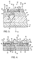
- FIG. 4 illustrates another hybrid transistor 90 embodying the present invention, in which like elements are designated by the same reference numerals as in FIGs. 2 and 3.
- the transistor 90 has an FET section 92 including FET structures 94.
- the structures 94 have a single channel layer MESFET configuration, including an N-type channel layer 96 and a Schottky gate 98.
- the channel layers 96 are 5,000 - 10,000 angstroms thick, with the preferred thickness being 7,500 angstroms.
- the layers 96 are doped with silicon to a concentration of 5 x 10¹⁷ - 1018 ions/cm3, with the preferred concentration being 7.5 x 10¹⁷.
- the Schottky gates 98 preferably include a lower layer of a refractory metal such as titanium which forms a Schottky barrier with the layer 96, and overlying ohmic contact layers of platinum and gold.
- FIG. 5 illustrates another hybrid transistor 100 embodying the invention, having an FET section 102 including FET structures 104 with a junction field-effect transistor (JFET) configuration.
- Each structure 104 includes an N-type layer 106 and a P-type layer 108 which form a P-N diode junction.
- An ohmic contact layer 110 is formed over the P-type layer.
- Ohmic contacts 112 are connected to the opposite ends of the N-type layer 106, as well as to the underlying collector layers 48 and cathode terminals 56.
- the transistor 100 may be fabricated as a homostructure in a single group III-V material, preferably GaAs or InP.
- the N-type layer 106 is 3,000 - 6,000 angstroms thick, with the preferred thickness being 4,500 angstroms.
- the layer 106 is doped with selenium (Se), silicon or tin (Sn) to a concentration of 5 x 10¹⁶ - 2 x 10¹⁷ ions/cm3 , with the preferred concentration being 8 x 10¹⁶ ions/cm3.
- the layer 108 is 2,500 - 5,000 angstroms thick, with the preferred thickness being 3,000 angstroms.
- the layer 108 is doped with beryllium or zinc to a concentration of concentration of 1018 - 1019 ions/cm3, with the preferred concentration being 5 x 10¹⁸ ions/cm3.
- FIG. 6 illustrates a transistor 120 including an FET section 122 having FET structures 124 operating with lateral modulation.
- This arrangement can be embodied in the HEMT, single or dual channel layer MESFET or JEFET configuration.
- the JFET configuration is illustrated in FIG. 6 as including two laterally spaced channel sections 126.
- Each section 126 includes an N-type channel layer 128 and an N+ contact layer 130 which is connected via a metallization 132 to the cathode terminals 56.
- the layers 128 and 130 are spaced laterally, rather than vertically as in the arrangement of FIG. 5, from the respective collector layers 48.
- the layers 128 are 1,000 - 2,000 angstroms thick, with the preferred thickness being 1,500 angstroms.
- the layer 128 is doped with beryllium to a concentration of 5 x 10¹⁸ - 1019, with the preferred concentration being 7.5 x 10¹⁸.
- Each FET structure 124 further includes a P+ layer 134 which can be fabricated simultaneously with the collector layers 48.
- the layer 134 is connected to the respective gate electrode 70 via a Schottky metal contact layer 136.
- the space surrounding the layers 134 and 136 and underlying a central portion of the metallization 132 which extends over the layers 134 and 136 is filled with an insulating polyamide material 138.
- the operation of the transistor 124 is similar to that of the transistor 104 illustrated in FIG. 5, except that the channel layer 128 is modulated laterally, rather than vertically, by the electric field extending from the P+ layer 134 and that portions of the injection regions 54 and insulating material 138 intervene between the channel layers 128 and the respective layers 134.
- the lateral modulation configuration ensures that the transistor 124 can be turned off hard due to the reduced lengths of the depletion regions in the channel layers 128 in the OFF state of the transistor 124.
- the method of fabricating a hybrid transistor as described above is not the particular subject matter of the present invention and will not be described in detail.
- the transistors illustrated in FIGs. 2 to 5 are most readily fabricated using epitaxial deposition and patterning for the semiconductor layers, whereas the transistor illustrated in FIG. 6 is most readily fabricated using epitaxial deposition of the layers 44 and 46 and ion implantation of the other layers.
- the present hybrid transistor has been described and illustrated as including a PNP bipolar transistor section and an N-channel FET section, it is within the scope of the invention to reverse the applicable conductivity types and voltages to provide a hybrid transistor including an NPN bipolar transistor section and a P-channel FET section.
- junction-gate FET of either channel conductivity type operating in either enhancement or depletion mode can be combined with a bipolar transistor of either conductivity type as long as the FET injects charge carriers of the required polarity into the base of the bipolar transistor for conductivity modulation. It is yet further within the scope of the invention to fabricate a hybrid transistor in a material system other than group III-V, such as silicon.
Abstract
A hybrid power transistor (40) includes a vertical PNP bipolar transistor (42) having a floating base (46). A junction-gate type field-effect transistor (FET) (62) has a lateral N-type channel (64, 66) and a vertical electron injection path (54) from the channel (64, 66) into the base (46) of the bipolar transistor (42). The FET channel current and thereby the electron injection current are controlled by the FET gate voltage. The injection current conductivity modulates the base (46) and thereby controls the collector current of the bipolar transistor (42). The FET (62) does not require a gate insulating layer, enabling fabrication of the hybrid transistor (40) in the group III-V material system.
Description
- The present invention generally relates to power transistors, and more specifically to a hybrid bipolar/field-effect power transistor fabricated in the group III-V material system.
- The insulated gate bipolar transistor (IGBT) is a hybrid power transistor which offers the high input impedance and low input current of a field-effect transistor, together with the high current capability of a bipolar transistor. A general description of the IGBT is presented in a textbook entitled "POWER TRANSISTORS: DEVICE DESIGN AND APPLICATIONS", edited by B. Jayant Baliga et al, IEEE Press, 1984, pp. 354-363.
- A
conventional IGBT 10 is illustrated in FIG. 1, and is fabricated in silicon. The IGBT 10 includes a bipolar PNPtype transistor section 12 including aP+ emitter layer 14, an N- base ordrift layer 16 and a plurality of laterally spacedP+ collector layers 18. Portions of thebase layer 16 extend upwardly into the lateral gaps between thecollector layers 18 to constitutevertical injection regions 20. - An
anode terminal 22 is ohmically connected to theemitter layer 14 via ametal contact layer 24.N+ regions 26 are formed in the opposite end portions of thecollector layers 18, and provide ohmic contact between thelayers 18 andcathode terminals 28 viametal contacts 30. - The IGBT 10 further includes a field-effect transistor (FET)
section 31 including a plurality of insulatedgate FET structures 32. Eachstructure 32 includes agate insulator layer 33 which is formed of silicon dioxide or silicon nitride and extends over theunderlying injection region 20 betweenadjacent N+ regions 26. Agate metal layer 34 is formed over eachinsulator layer 33 to provide a metal-oxide-semiconductor (MOS) gate structure. - The
metal layers 34 are connected togate terminals 36. For high power operation, thecathode terminals 28 are connected together and thegate terminals 36 are connected together. Thecathode terminals 28 are grounded, and a positive voltage is applied to theanode terminal 22. - With zero voltage applied to the
gate terminals 36,lateral channels 38 defined in the upper portions of thecollector layers 18 under thegate insulator layers 33 between the adjacent lateral edges of theN+ regions 26 and thecollector layers 18 are depleted of electrons, and no electron current flows through thechannels 38. - Application of a sufficiently high positive voltage to the
gate terminals 36 enhances (attracts electrons into) thechannels 38 and the upper portions of theinjection regions 20 which constitute extensions of thechannels 38. This creates a lateral conduction path from theN+ regions 26 into theinjection regions 20 through thechannels 38. - Electrons are injected from the
cathode terminals 28 through the lateral conduction path from which they are vertically injected into theinjection regions 20. The electrons drift downwardly from theregions 20 through thebase layer 16 andemitter layer 14 toward and are collected at theanode terminal 22. The electron flow through thebase layer 16 increases the conductivity thereof, and causes holes to be back injected from theanode 22 andemitter layer 14 into thebase layer 16, from which they flow through thecollector layers 18 to thecathode terminals 28. - The hole current from the
anode terminal 22 through theemitter layer 14,base layer 16 andcollector layers 18 to thecathode terminals 28 constitutes the main power current of theIGBT 10. Thebase layer 16 is conductivity modulated by the electron current which is vertically injected into theregions 20 from thechannel regions 38 of theFET section 31. The larger the electron injection current, the higher the conductivity of thebase layer 16 and the higher the hole current of thebipolar transistor section 12. - The
FET section 31 has an insulated gate or MOS structure, as this enables the highest power operation of the various field-effect transistor configurations using silicon technology. However, the conventional silicon IGBT has relatively low electron mobility, which produces a high forward voltage drop across the device and accompanying power loss. - In addition, the low bandgap of silicon produces a relatively low breakdown voltage. Another problem inherent in silicon IGBTs is a latch-up phenomenon caused by parasitic NPH transistor or PNPN thyristor action. These drawbacks prevent the silicon IGBT from being used in applications such as power switches in which these limitations are unacceptable.
- Transistor devices fabricated in group III-V material systems, including gallium arsenide (GaAs) and indium phosphide (InP), have higher electron mobility, higher breakdown voltage, higher operating speed and lower losses. However, the IGBT design cannot be practically implemented in a group III-V material system as it requires the
gate insulator layers 33 which are difficult or impossible to fabricate on group III-V materials. - A hybrid power transistor embodying the present invention includes a vertical PNP bipolar transistor having a floating base. A junction-gate type field-effect transistor (FET) has a lateral N-type channel and a vertical electron injection path from the channel into the base of the bipolar transistor.
- The FET channel current and thereby the electron injection current are controlled by the FET gate voltage. The injection current conductivity modulates the base and thereby controls the collector current of the bipolar transistor. The FET may have a high electron mobility transistor (HEMT), junction-gate field-effect transistor (JFET) or metal-semiconductor field-effect transistor (MESFET) structure.
- The junction-gate FET of the present transistor does not require a gate insulating layer, enabling fabrication of the transistor in a group III-V material system. This enables the present transistor to embody the advantages of group III-V devices, including higher electron mobility, higher current density, higher breakdown voltage, higher operating speed and lower losses than the prior art IGBT.
- The HEMT configuration has a channel and gate structure including a doped, wide bandgap material layer formed over a substantially intrinsic narrow bandgap material layer. These two layers form a heterojunction. This embodiment of the invention is designated as a "heterojunction gate bipolar transistor (HGBT)".
- The present hybrid transistor, especially in the HEMT configuration, is substantially less prone to latch-up than the IGBT. The narrow bandgap layer reduces the emitter efficiency of the parasitic NPN transistor, thereby reducing its current gain and latch-up tendency. With appropriate design, the present transistor can be made substantially latch-up free.
- These and other features and advantages of the present invention will be apparent to those skilled in the art from the following detailed description, taken together with the accompanying drawings, in which like reference numerals refer to like parts.
-
- FIG. 1 is a simplified sectional view illustrating a prior art insulated-gate bipolar transistor (IGBT);
- FIG. 2 is a simplified sectional view illustrating a hybrid bipolar/field-effect transistor embodying the present invention including a high electron mobility transistor (HEMT) or dual doped layer metal-semiconductor transistor (MESFET) channel structure;
- FIG. 3 is an enlarged sectional view illustrating electron and hole flow in the transistor of FIG. 2;
- FIG. 4 is a simplified sectional view of a hybrid bipolar/field-effect transistor embodying the present invention including a single doped layer MESFET channel structure;
- FIG. 5 illustrates a hybrid bipolar/field-effect transistor embodying the present invention including a junction field-effect transistor (JFET) channel and gate structure with vertical modulation; and
- FIG. 6 illustrates a hybrid bipolar/field-effect transistor embodying the present invention including a junction field-effect transistor (JFET) channel and gate structure with lateral modulation.
- A
hybrid power transistor 40 embodying the present invention is illustrated in FIG. 2. Thetransistor 40 includes a PNPbipolar transistor section 42 including aP+ emitter layer 44, an N- base ordrift layer 46, and laterally spacedcollector layers 48 which are analogous to thelayers IGBT 10 as described above with reference to FIG. 1. - The
bipolar transistor section 42 is preferably fabricated in the group III-V material system, with thelayers anode terminal 50 is connected to theemitter layer 44 via ametal contact layer 52. - Portions of the
base layer 46 extend upwardly into the lateral gaps betweenadjacent collector layers 48 to define verticalelectron injection regions 54.Cathode terminals 56 are ohmically connected to thecollector layers 48 viametal contacts 58. - The
transistor 40 further includes anFET section 60 including a plurality ofFET structures 62. Eachstructure 62 has a heterojunction channel including a substantially intrinsiclower layer 64 of a narrow bandgap material, preferably gallium indium arsenide (GaInAs), and an N-typeupper layer 66 of a wide bandgap material, preferably aluminum gallium arsenide (AlGaAs) or aluminum indium arsenide (AlInAs). A Schottkymetal gate 68 is formed on eachlayer 66 and connected to agate terminal 70. Due to the heterojunction structure, thetransistor 40 is designated as a "heterojunction gate bipolar transistor (HGBT)". - The
layers gate 68 of eachFET structure 62 have the configuration of a high electron mobility transistor (HEMT). Thetransistor 40 further includesohmic contacts 72 which are formed on the opposite ends of thelayers 66 and are connected to thecathode terminals 56. - For high power operation, the
cathode terminals 56 are grounded and a positive voltage is applied to theanode terminal 50. TheFET section 60 is preferably operated in depletion mode, with a negative control signal applied to thegate terminals 70, although enhancement mode operation is also possible. - The operation of the
transistor 40 will be described with reference also being made to FIG. 3. With a sufficiently negative signal applied to thegate terminals 70, the Schottky junction of thelayer 66 andgate 68 is reverse biased and thelayer 64 is depleted of electrons, such that no electrons are injected from theFET structures 62 into theinjection regions 54. - When the negative gate voltage reduced to a sufficient level, the reverse bias of the Schottky junction is reduced and the depletion of the
layer 64 is also reduced to an extent that a two-dimensional electron gas (2DEG)layer 74 is formed in thelayer 64 just below the interface with thelayer 66. The2DEG layer 74 provides a lateral conduction path between thecontacts 72 at the opposite ends of eachlayer structure cathode terminals 72 into the2DEG layer 74 as indicated byarrows 76, flow through thelayer 74, and are injected vertically into theinjection regions 54 as indicated by arrows 78. - The injected electrons drift downwardly through the
base layer 46 andemitter layer 44 and are collected at theanode terminal 50. This causes back injection of holes from theemitter layer 44 into thebase layer 46 as indicated by arrows 80. The injected holes flow upwardly through the collector layers 48 to thecathode terminals 56. - The hole current from the
anode terminal 50 through theemitter layer 44,base layer 46 and collector layers 48 to thecathode terminals 56 constitutes the main power current of thetransistor 40. Thebase layer 46 is conductivity modulated by the electron current which is vertically injected into theregions 54 from the2DEG layer 74 of theFET structures 62. The larger the electron injection current, the higher the conductivity of thebase layer 46 and the higher the hole current of thebipolar transistor section 42. - It will be noted that although each
FET structure 62 has a source (one of the contacts 72), a lateral channel (layers 64 and 66) and a drain (the other of the contacts 72), the source and drain are both connected to ground (the cathode terminals 56). In the present configuration, therefore, eachFET structure 62 can be considered as constituting two FETs, with a source (one of the contacts 72), a channel (the lateral half of thelayers - It will be further noted that the operation of the
transistor 40 is facilitated by the symmetrical arrangement as illustrated in which one N-channel FET structure 62 is provided for injecting electrons into two vertical PNP bipolar transistors on opposite lateral sides of therespective FET structure 62. However, it is theoretically possible, and within the scope of the invention, to fabricate a hybrid transistor including only one vertical bipolar transistor and one FET. - The electron mobility in the HEMT heterojunction channel and gate configuration is extremely high, at least an order of magnitude higher than in the prior art silicon IGBT. The high electron mobility produces a lower forward voltage drop and higher current density than are possible with the IGBT.
- In addition, the narrow bandgap material of the upper channel layers 66 reduces the emitter injection efficiency of the parasitic NPN transistor constituted by the
base layer 46, collector layers 48 and channel layers 66, reducing its current gain and producing substantially latch-up free operation. Thetransistor 40 also benefits from the inherent advantages of group III-V devices, including high breakdown voltage and high operating speed. - The preferred dimensions and doping concentrations for the
transistor 40 are given below, but should not be considered as limiting the scope of the invention. - The
emitter layer 44 is 0.5 - 2.0 micrometers thick, with the preferred thickness being 1.0 micrometer. Thelayer 44 is doped with beryllium (Be) or zinc (Zn) to a concentration of 5 x 10¹⁸ - 5 x 10¹⁹ ions/cm³, with the preferred concentration being 10¹⁹. - The
base layer 46 is 20 - 30 micrometers thick, with the preferred thickness being 25 micrometers. Thelayer 46 is doped as lightly as possible, preferably intrinsic, with the impurity concentration being less than 10¹⁴ - 10¹⁵ ions/cm³. - The collector layers 48 are 3,000 - 8,000 angstroms thick, with the preferred thickness being 5,000 angstroms. The length of the lateral gap (the horizontal length of the
injection regions 54 as viewed in FIGs. 2 and 3) is 2 - 10 micrometers. Thelayers 48 are doped with beryllium or zinc to a concentration of 5 x 10¹⁸ - 5 x 10¹⁹ ions/cm³, with the preferred concentration being 10¹⁹. - The narrow
bandgap channel layer 64 is intrinsic and 200 - 1,000 angstroms thick, with the preferred thickness being 500 angstroms. The widebandgap channel layer 66 is 500 - 2,000 angstroms thick, with the preferred thickness being 1,000 angstroms. Thelayer 66 is doped with silicon (Si) to a concentration of 2 x 10¹⁷ - 2 x 10¹⁸ ions/cm³, with the preferred concentration being 5 x 10¹⁷. - The
FET structures 62 can alternatively be embodied as metal-semiconductor transistor (MESFET) structures having dual channel layers using the same materials as the HEMT configuration by selecting different layer thicknesses and doping concentrations. In the MESFET embodiment, thelayer 64 functions as an N-type channel layer, whereas thelayer 66 functions as a Schottky layer. Electrons are vertically injected from thelayer 64 into theinjection regions 54 to conductivity modulate thebase layer 46 as described above. - For the dual channel layer MESFET configuration, the
layer 64 is 300 - 1,000 angstroms thick, with the preferred thickness being 500 angstroms. Thelayer 64 is doped with silicon (Si) to a concentration of 2 x 10¹⁷ - 10¹⁸ ions/cm³, with the preferred concentration being 5 x 10¹⁷. Thelayer 66 is undoped and has a thickness of 1,000 - 3,000 angstroms, with the preferred thickness being 2,000 angstroms. - FIG. 4 illustrates another
hybrid transistor 90 embodying the present invention, in which like elements are designated by the same reference numerals as in FIGs. 2 and 3. Thetransistor 90 has anFET section 92 includingFET structures 94. In thetransistor 90, thestructures 94 have a single channel layer MESFET configuration, including an N-type channel layer 96 and aSchottky gate 98. - The channel layers 96 are 5,000 - 10,000 angstroms thick, with the preferred thickness being 7,500 angstroms. The
layers 96 are doped with silicon to a concentration of 5 x 10¹⁷ - 10¹⁸ ions/cm³, with the preferred concentration being 7.5 x 10¹⁷. Although not illustrated in detail, theSchottky gates 98 preferably include a lower layer of a refractory metal such as titanium which forms a Schottky barrier with thelayer 96, and overlying ohmic contact layers of platinum and gold. - FIG. 5 illustrates another
hybrid transistor 100 embodying the invention, having anFET section 102 includingFET structures 104 with a junction field-effect transistor (JFET) configuration. Eachstructure 104 includes an N-type layer 106 and a P-type layer 108 which form a P-N diode junction. Anohmic contact layer 110 is formed over the P-type layer.Ohmic contacts 112 are connected to the opposite ends of the N-type layer 106, as well as to the underlying collector layers 48 andcathode terminals 56. - The
transistor 100 may be fabricated as a homostructure in a single group III-V material, preferably GaAs or InP. The N-type layer 106 is 3,000 - 6,000 angstroms thick, with the preferred thickness being 4,500 angstroms. Thelayer 106 is doped with selenium (Se), silicon or tin (Sn) to a concentration of 5 x 10¹⁶ - 2 x 10¹⁷ ions/cm³, with the preferred concentration being 8 x 10¹⁶ ions/cm³. - The
layer 108 is 2,500 - 5,000 angstroms thick, with the preferred thickness being 3,000 angstroms. Thelayer 108 is doped with beryllium or zinc to a concentration of concentration of 10¹⁸ - 10¹⁹ ions/cm³, with the preferred concentration being 5 x 10¹⁸ ions/cm³. - Whereas the hybrid transistors embodying the present invention described above include FET structures which operate with vertical modulation, FIG. 6 illustrates a
transistor 120 including anFET section 122 havingFET structures 124 operating with lateral modulation. This arrangement can be embodied in the HEMT, single or dual channel layer MESFET or JEFET configuration. - The JFET configuration is illustrated in FIG. 6 as including two laterally spaced
channel sections 126. Eachsection 126 includes an N-type channel layer 128 and anN+ contact layer 130 which is connected via ametallization 132 to thecathode terminals 56. Thelayers layers 128 are 1,000 - 2,000 angstroms thick, with the preferred thickness being 1,500 angstroms. Thelayer 128 is doped with beryllium to a concentration of 5 x 10¹⁸ - 10¹⁹, with the preferred concentration being 7.5 x 10¹⁸. - Each
FET structure 124 further includes aP+ layer 134 which can be fabricated simultaneously with the collector layers 48. Thelayer 134 is connected to therespective gate electrode 70 via a Schottkymetal contact layer 136. The space surrounding thelayers metallization 132 which extends over thelayers polyamide material 138. - The operation of the
transistor 124 is similar to that of thetransistor 104 illustrated in FIG. 5, except that thechannel layer 128 is modulated laterally, rather than vertically, by the electric field extending from theP+ layer 134 and that portions of theinjection regions 54 and insulatingmaterial 138 intervene between the channel layers 128 and the respective layers 134. The lateral modulation configuration ensures that thetransistor 124 can be turned off hard due to the reduced lengths of the depletion regions in the channel layers 128 in the OFF state of thetransistor 124. - The method of fabricating a hybrid transistor as described above is not the particular subject matter of the present invention and will not be described in detail. However, the transistors illustrated in FIGs. 2 to 5 are most readily fabricated using epitaxial deposition and patterning for the semiconductor layers, whereas the transistor illustrated in FIG. 6 is most readily fabricated using epitaxial deposition of the
layers - While several illustrative embodiments of the invention have been shown and described, numerous variations and alternate embodiments will occur to those skilled in the art, without departing from the spirit and scope of the invention.
- For example, although the present hybrid transistor has been described and illustrated as including a PNP bipolar transistor section and an N-channel FET section, it is within the scope of the invention to reverse the applicable conductivity types and voltages to provide a hybrid transistor including an NPN bipolar transistor section and a P-channel FET section.
- Further, a junction-gate FET of either channel conductivity type operating in either enhancement or depletion mode can be combined with a bipolar transistor of either conductivity type as long as the FET injects charge carriers of the required polarity into the base of the bipolar transistor for conductivity modulation. It is yet further within the scope of the invention to fabricate a hybrid transistor in a material system other than group III-V, such as silicon.
- Accordingly, it is intended that the present invention not be limited solely to the specifically described illustrative embodiments. Various modifications are contemplated and can be made without departing from the spirit and scope of the invention as defined by the appended claims.
Claims (33)
- A hybrid transistor (40; 90; 100; 110), comprising: vertical bipolar transistor means (42, 44, 46, 48) having a collector (48), an emitter (44) and a floating base (46); and
junction-gate type field-effect transistor means (62; 94; 104; 124) having a lateral channel (64, 66; 96; 106, 108; 128, 130), means (72; 112) for directing current through said channel (64, 66; 96; 106, 108; 128, 130), and a vertical charge carrier injection path (78) from the channel (64, 66; 96; 106, 108; 128, 130) into the base (46, 54) of said vertical bipolar transistor means (42, 44, 46, 48). - The hybrid transistor (40; 90; 100; 110) of claim 1, characterized in that the bipolar transistor means (42, 44, 46, 48) and the field-effect transistor means (62; 94; 104; 124) are formed of group III-V materials.
- The hybrid transistor (40; 90; 100; 110) of claim 1 or claim 2, characterized in that the channel (64, 66; 96; 106, 108; 128, 130) comprises a heterojunction structure (64, 66).
- The hybrid transistor (40; 90; 100; 110) of any of claims 1 - 3, characterized in that the field-effect transistor means (62; 94; 104; 124) comprises a high electron mobility transistor (HEMT) structure (62) or a junction field-effect transistor (JFET) structure (104) or a metal-semiconductor field-effect transistor (MESFET) structure (94).
- The hybrid transistor (40; 90; 100; 110) of any of claims 1 - 4, characterized in that the bipolar transistor means (42, 44, 46, 48) is PNP type and the field-effect transistor means (62; 94; 104; 124) is N-channel type.
- The hybrid transistor (40; 90; 100; 110) of any of claims 1 - 5, characterized in that
the vertical bipolar transistor means (42, 44, 46, 48) has a layer of one conductivity type for the emitter (44), a layer of opposite conductivity to said emitter layer (44) formed over the emitter layer (44) and forming the floating base (46);
and two laterally spaced collector layers (48) of like conductivity to said emitter layer (44) which are formed over the base layer (46) and define a lateral gap therebetween and forming a collector, a portion (54) of the base layer (46) extending into said gap to constitute an injection region (54); and that
the field-effect transistor means (62; 94; 104; 124) has the lateral channel (64, 66; 96; 106, 108; 128, 130) of opposite conductivity to said emitter layer (44) formed over said injection region (54); and
a junction-type gate (68; 98; 110; 132, 136) formed over the channel (64, 66; 96; 106, 108; 128, 130), the gate (68; 98; 110; 132, 136) controlling vertical injection of electrons from the channel (64, 66; 96; 106, 108; 128, 130) into said injection region (54) and thereby conductivity modulation of the base layer (46). - The hybrid transistor (40; 90; 100; 110) of claim 6, further characterized by
a cathode terminal (56) connected to the collector layers (48);
an anode terminal (50) connected to the emitter layer (44); and
a gate terminal (70) connected to the gate layer (68; 98; 110; 132, 136). - The hybrid transistor (40; 90; 100; 110) of any of claims 1 - 7, characterized in that emitter, base and collector layers (44, 46, 48) of the bipolar transistor means (42, 44, 46, 48) are formed of a material selected from the group consisting of gallium arsenide (GaAs) and indium phosphide (InP).
- The hybrid transistor (40; 90; 100; 110) of claim 6 or claim 6 and claim 7 or claim 8, characterized in that said gap has a length of approximately 2 - 10 micrometers.
- The hybrid transistor (40; 90; 100; 110) of claim 6 or claim 6 and any of claims 7 - 9, characterized in that the channel (64, 66; 96; 106, 108; 128, 130) comprises a high electron mobility transistor (HEMT) structure (62) including:
a narrow bandgap material layer (64) formed over the injection region (54); and
a wide bandgap material layer (66) formed over the narrow bandgap material layer (64). - The hybrid transistor (40; 90; 100; 110) of claim 10, characterized in that the narrow bandgap material layer (64) comprises gallium indium arsenide (GaInAs).
- The hybrid transistor (40; 90; 100; 110) of claim 10 or claim 11, characterized in that the narrow bandgap material layer (64) has a thickness of approximately 200 - 1,000 angstroms.
- The hybrid transistor (40; 90; 100; 110) of any of claims 10 - 12, characterized in that the narrow bandgap material layer (64) is substantially intrinsic.
- The hybrid transistor (40; 90; 100; 110) of any of claims 10 - 13, characterized in that the wide bandgap material layer (66) comprises a material selected from the group consisting of aluminum gallium arsenide (AlGaAs) and aluminum indium arsenide (AlInAs).
- The hybrid transistor (40; 90; 100; 110) of any of claims 10 - 14, characterized in that the wide bandgap material layer (66) has a thickness of approximately 500 - 2,000 angstroms.
- The hybrid transistor (40; 90; 100; 110) of any of claims 10 - 15, characterized in that the wide bandgap material layer (66) is doped with silicon (Si) to a concentration of approximately 2 x 10¹⁷ - 2 x 10¹⁸ ions/cm³.
- The hybrid transistor (40; 90; 100; 110) of any of claims 10 - 16, characterized in that the gate (68; 98; 110; 132, 136) comprises a material (68) which forms a Schottky barrier with the wide bandgap material layer (66).
- The hybrid transistor (40; 90; 100; 110) of any of claims 6 - 9, characterized in that said emitter layer (44) is N-type and the channel (64, 66; 96; 106, 108; 128, 130) comprises a junction field-effect transistor (JFET) structure (104) including:
an N-type layer (106) formed over the injection region (54); and
a P-type layer (108) formed over the N-type layer (106). - The hybrid transistor (40; 90; 100; 110) of any of claims 10 - 18, characterized in that the layers (64, 66; 106, 108) of said channel (64, 66; 96; 106, 108; 128, 130) are formed of a material selected from the group consisting of gallium arsenide (GaAs) and indium phosphide (InP).
- The hybrid transistor (40; 90; 100; 110) of claim 18 or claim 18 and claim 19, characterized in that the N-type layer (106) of said channel (64, 66; 96; 106, 108; 128, 130) has a thickness of approximately 3,000 - 6,000 angstroms.
- The hybrid transistor (40; 90; 100; 110) of claim 18 or claim 20, characterized in that the N-type layer (106) of said channel (64, 66; 96; 106, 108; 128, 130) is doped with a material selected from the group consisting of selenium (Se), silicon (Si) and tin (Sn) to a concentration of approximately 5 x 10¹⁶ - 2 x 10¹⁷ ions/cm³.
- The hybrid transistor (40; 90; 100; 110) of claim 18 or claim 18 and any of claims 19 - 21, characterized in that the P-type layer (108) of said channel (64, 66; 96; 106, 108; 128, 130) has a thickness of approximately 2,500 - 5,000 angstroms.
- The hybrid transistor (40; 90; 100; 110) of claim 18 or claim 18 and any of claims 19 - 22, characterized in that the P-type layer (108) of said channel (64, 66; 96; 106, 108; 128, 130) is doped with a material selected from the group consisting of beryllium (Be) and zinc (Zn) to a concentration of approximately 10¹⁸ - 10¹⁹ ions/cm³.
- The hybrid transistor (40; 90; 100; 110) of any of claims 6 - 9, characterized in that the channel (64, 66; 96; 106, 108; 128, 130) comprises a metal semiconductor field-effect transistor (MESFET) structure including:
an N-type channel layer (64; 96) formed over the injection region (54); and
a Schottky layer (66; 98) formed over the channel layer (96). - The hybrid transistor (40; 90; 100; 110) of claim 24, characterized in that the channel layer (64) has a thickness of approximately 300 - 1,000 angstroms.
- The hybrid transistor (40; 90; 100; 110) of claim 24 or claim 25, characterized in that the Schottky layer (66) is formed of a material selected from the group consisting of gallium arsenide (GaAs) and aluminum gallium arsenide (AlGaAs).
- The hybrid transistor (40; 90; 100; 110) of any of claims 24 - 26, characterized in that the Schottky layer (66) is substantially intrinsic.
- The hybrid transistor (40; 90; 100; 110) of any of claims 24 - 27, characterized in that the Schottky layer (66) has a thickness of approximately 1,000 - 3,000 angstroms.
- The hybrid transistor (40; 90; 100; 110) of any of claims 24 - 28, characterized in that the channel layer (64) is formed of a group III-V material and the Schottky layer (66) is formed of a metal which forms a Schottky barrier with the channel layer (64).
- The hybrid transistor (40; 90; 100; 110) of claim 24, characterized in that the channel layer (96) is formed of gallium indium arsenide (GaInAs).
- The hybrid transistor (40; 90; 100; 110) of claim 30, characterized in that the channel layer (96) is formed of a group III-V material and has a thickness of approximately 5,000 - 10,000 angstroms.
- The hybrid transistor (40; 90; 100; 110) of claim 30 or claim 31, characterized in that the channel layer (96) is doped with silicon (Si) to a concentration of approximately 2 x 10¹⁷ - 10¹⁸ ions/cm³.
- The hybrid transistor (40; 90; 100; 110) of any of claims 6 - 9, characterized in that
the channel (64, 66; 96; 106, 108; 128, 130) comprises two laterally spaced sections (126) which define a lateral gap therebetween; and
the gate (136) extends through said gap between the channel sections (126) into the injection region (54) to laterally modulate electron flow through the channel (64, 66; 96; 106, 108; 128, 130).
Applications Claiming Priority (2)
| Application Number | Priority Date | Filing Date | Title |
|---|---|---|---|
| US07/994,734 US5359220A (en) | 1992-12-22 | 1992-12-22 | Hybrid bipolar/field-effect power transistor in group III-V material system |
| US994734 | 1997-12-19 |
Publications (1)
| Publication Number | Publication Date |
|---|---|
| EP0603737A2 true EP0603737A2 (en) | 1994-06-29 |
Family
ID=25540989
Family Applications (1)
| Application Number | Title | Priority Date | Filing Date |
|---|---|---|---|
| EP93120248A Withdrawn EP0603737A2 (en) | 1992-12-22 | 1993-12-16 | Hybrid bipolar/field-effect power transistor in group III-V material system |
Country Status (6)
| Country | Link |
|---|---|
| US (1) | US5359220A (en) |
| EP (1) | EP0603737A2 (en) |
| JP (1) | JPH0714845A (en) |
| KR (1) | KR940016780A (en) |
| CA (1) | CA2111788A1 (en) |
| MX (1) | MX9308181A (en) |
Cited By (4)
| Publication number | Priority date | Publication date | Assignee | Title |
|---|---|---|---|---|
| US5777353A (en) * | 1995-11-09 | 1998-07-07 | National Science Council | Multiple-function gaas transistors with very strong negative differential resistance phenomena |
| EP2866251A4 (en) * | 2012-06-26 | 2016-03-02 | Sumitomo Electric Industries | Silicon carbide semiconductor device |
| DE102016015475B3 (en) * | 2016-12-28 | 2018-01-11 | 3-5 Power Electronics GmbH | IGBT semiconductor structure |
| EP3937253A1 (en) | 2020-07-06 | 2022-01-12 | AZUR SPACE Solar Power GmbH | Vertical high blocking iii-v bipolar transistor |
Families Citing this family (15)
| Publication number | Priority date | Publication date | Assignee | Title |
|---|---|---|---|---|
| US5767546A (en) * | 1994-12-30 | 1998-06-16 | Siliconix Incorporated | Laternal power mosfet having metal strap layer to reduce distributed resistance |
| US5665996A (en) * | 1994-12-30 | 1997-09-09 | Siliconix Incorporated | Vertical power mosfet having thick metal layer to reduce distributed resistance |
| SE512661C2 (en) * | 1996-11-13 | 2000-04-17 | Ericsson Telefon Ab L M | Lateral bipolar hybrid transistor with field effect mode and method at the same |
| US6972448B2 (en) * | 2000-12-31 | 2005-12-06 | Texas Instruments Incorporated | Sub-lithographics opening for back contact or back gate |
| CA2456662A1 (en) * | 2001-08-07 | 2003-02-20 | Jan Kuzmik | High electron mobility devices |
| JP4645753B2 (en) * | 2003-02-06 | 2011-03-09 | 株式会社豊田中央研究所 | Semiconductor device having group III nitride semiconductor |
| JP4645034B2 (en) * | 2003-02-06 | 2011-03-09 | 株式会社豊田中央研究所 | Semiconductor device having group III nitride semiconductor |
| TWI295085B (en) * | 2003-12-05 | 2008-03-21 | Int Rectifier Corp | Field effect transistor with enhanced insulator structure |
| JP2005317830A (en) * | 2004-04-30 | 2005-11-10 | Elpida Memory Inc | Semiconductor device, multi chip package, and wire bonding method |
| JP4650224B2 (en) * | 2004-11-19 | 2011-03-16 | 日亜化学工業株式会社 | Field effect transistor |
| US7411226B2 (en) * | 2005-04-27 | 2008-08-12 | Northrop Grumman Corporation | High electron mobility transistor (HEMT) structure with refractory gate metal |
| KR101108746B1 (en) * | 2010-07-07 | 2012-02-24 | 삼성전기주식회사 | Nitride based semiconductor device and method for manufacturing the same |
| US20150108500A1 (en) * | 2013-10-18 | 2015-04-23 | Infineon Technologies Austria Ag | Semiconductor Device and Method of Manufacturing the Same |
| US9793430B1 (en) * | 2016-05-09 | 2017-10-17 | Qatar University | Heterojunction schottky gate bipolar transistor |
| US10468503B1 (en) * | 2018-05-15 | 2019-11-05 | International Business Machines Corporation | Stacked vertical transport field effect transistor electrically erasable programmable read only memory (EEPROM) devices |
Family Cites Families (3)
| Publication number | Priority date | Publication date | Assignee | Title |
|---|---|---|---|---|
| JPS54145486A (en) * | 1978-05-08 | 1979-11-13 | Handotai Kenkyu Shinkokai | Gaas semiconductor device |
| FR2507820A1 (en) * | 1981-06-16 | 1982-12-17 | Thomson Csf | BIPOLAR FIELD EFFECT CONTROL TRANSISTOR USING ISLE GRID |
| US5068705A (en) * | 1990-07-31 | 1991-11-26 | Texas Instruments Incorporated | Junction field effect transistor with bipolar device and method |
-
1992
- 1992-12-22 US US07/994,734 patent/US5359220A/en not_active Expired - Lifetime
-
1993
- 1993-12-16 EP EP93120248A patent/EP0603737A2/en not_active Withdrawn
- 1993-12-17 MX MX9308181A patent/MX9308181A/en unknown
- 1993-12-17 CA CA002111788A patent/CA2111788A1/en not_active Abandoned
- 1993-12-21 KR KR1019930028896A patent/KR940016780A/en not_active Application Discontinuation
- 1993-12-22 JP JP5325114A patent/JPH0714845A/en active Pending
Cited By (12)
| Publication number | Priority date | Publication date | Assignee | Title |
|---|---|---|---|---|
| US5777353A (en) * | 1995-11-09 | 1998-07-07 | National Science Council | Multiple-function gaas transistors with very strong negative differential resistance phenomena |
| US6043518A (en) * | 1995-11-09 | 2000-03-28 | National Science Council | Multiple-function GaAs transistors with very strong negative differential resistance phenomena |
| EP2866251A4 (en) * | 2012-06-26 | 2016-03-02 | Sumitomo Electric Industries | Silicon carbide semiconductor device |
| DE102016015475B3 (en) * | 2016-12-28 | 2018-01-11 | 3-5 Power Electronics GmbH | IGBT semiconductor structure |
| US20180182874A1 (en) * | 2016-12-28 | 2018-06-28 | 3-5 Power Electronics GmbH | Igbt semiconductor structure |
| EP3343636A1 (en) * | 2016-12-28 | 2018-07-04 | 3-5 Power Electronics GmbH | Igbt semiconductor structure |
| CN108258030A (en) * | 2016-12-28 | 2018-07-06 | 3-5电力电子有限责任公司 | IGBT semiconductor structures |
| US11171226B2 (en) | 2016-12-28 | 2021-11-09 | 3-5 Power Electronics GmbH | GaAS based IGBT semiconductor structure |
| EP3937253A1 (en) | 2020-07-06 | 2022-01-12 | AZUR SPACE Solar Power GmbH | Vertical high blocking iii-v bipolar transistor |
| DE102020004051A1 (en) | 2020-07-06 | 2022-01-13 | Azur Space Solar Power Gmbh | Vertical high blocking III-V bipolar transistor |
| DE102020004051B4 (en) | 2020-07-06 | 2022-04-07 | Azur Space Solar Power Gmbh | Vertical high blocking III-V bipolar transistor |
| US11557665B2 (en) | 2020-07-06 | 2023-01-17 | Azur Space Solar Power Gmbh | Vertical high-blocking III-V bipolar transistor |
Also Published As
| Publication number | Publication date |
|---|---|
| JPH0714845A (en) | 1995-01-17 |
| US5359220A (en) | 1994-10-25 |
| KR940016780A (en) | 1994-07-25 |
| MX9308181A (en) | 1995-01-31 |
| CA2111788A1 (en) | 1994-06-23 |
Similar Documents
| Publication | Publication Date | Title |
|---|---|---|
| US5359220A (en) | Hybrid bipolar/field-effect power transistor in group III-V material system | |
| US4636823A (en) | Vertical Schottky barrier gate field-effect transistor in GaAs/GaAlAs | |
| US7982239B2 (en) | Power switching transistors | |
| US4641161A (en) | Heterojunction device | |
| US4485392A (en) | Lateral junction field effect transistor device | |
| EP0633611B1 (en) | Semiconductor device comprising an insulated-gate bipolar field-effect device | |
| US6066863A (en) | Lateral semiconductor arrangement for power IGS | |
| US5444272A (en) | Three-terminal thyristor with single MOS-gate controlled characteristics | |
| KR100204688B1 (en) | Heterojunction field effect transistor | |
| US5631483A (en) | Power device integrated structure with low saturation voltage | |
| US4989058A (en) | Fast switching lateral insulated gate transistors | |
| US4694313A (en) | Conductivity modulated semiconductor structure | |
| EP0615292A1 (en) | Insulated gate bipolar transistor | |
| JPH09321290A (en) | Semiconductor device with insulted gate bipolar transistor | |
| EP0228107B1 (en) | Fast switching lateral insulated gate transistors | |
| JPH10294461A (en) | Insulation gate type semiconductor element | |
| US5723349A (en) | Process for manufacturing a high conductivity insulated gate bipolar transistor integrater structure | |
| US5455442A (en) | COMFET switch and method | |
| US4903091A (en) | Heterojunction transistor having bipolar characteristics | |
| EP0115098A1 (en) | Lateral DMOS transistor device having an injector region | |
| EP0092645B1 (en) | Transistor and circuit including a transistor | |
| US4987469A (en) | Lateral high-voltage transistor suitable for use in emitter followers | |
| US11610987B2 (en) | NPNP layered MOS-gated trench device having lowered operating voltage | |
| JP3232763B2 (en) | Semiconductor device and driving method thereof | |
| JP3289880B2 (en) | MOS control thyristor |
Legal Events
| Date | Code | Title | Description |
|---|---|---|---|
| PUAI | Public reference made under article 153(3) epc to a published international application that has entered the european phase |
Free format text: ORIGINAL CODE: 0009012 |
|
| AK | Designated contracting states |
Kind code of ref document: A2 Designated state(s): DE FR GB IT SE |
|
| STAA | Information on the status of an ep patent application or granted ep patent |
Free format text: STATUS: THE APPLICATION HAS BEEN WITHDRAWN |
|
| 18W | Application withdrawn |
Withdrawal date: 19940824 |