EP0603070B1 - Procédé et dispositif pour la convolution analogique d'images - Google Patents
Procédé et dispositif pour la convolution analogique d'images Download PDFInfo
- Publication number
- EP0603070B1 EP0603070B1 EP93403037A EP93403037A EP0603070B1 EP 0603070 B1 EP0603070 B1 EP 0603070B1 EP 93403037 A EP93403037 A EP 93403037A EP 93403037 A EP93403037 A EP 93403037A EP 0603070 B1 EP0603070 B1 EP 0603070B1
- Authority
- EP
- European Patent Office
- Prior art keywords
- capacitors
- network
- terminals
- capacitor
- image
- Prior art date
- Legal status (The legal status is an assumption and is not a legal conclusion. Google has not performed a legal analysis and makes no representation as to the accuracy of the status listed.)
- Expired - Lifetime
Links
Images


Classifications
-
- G—PHYSICS
- G06—COMPUTING OR CALCULATING; COUNTING
- G06G—ANALOGUE COMPUTERS
- G06G7/00—Devices in which the computing operation is performed by varying electric or magnetic quantities
- G06G7/12—Arrangements for performing computing operations, e.g. operational amplifiers specially adapted therefor
- G06G7/19—Arrangements for performing computing operations, e.g. operational amplifiers specially adapted therefor for forming integrals of products, e.g. Fourier integrals, Laplace integrals or correlation integrals; for analysis or synthesis of functions using orthogonal functions
- G06G7/1907—Arrangements for performing computing operations, e.g. operational amplifiers specially adapted therefor for forming integrals of products, e.g. Fourier integrals, Laplace integrals or correlation integrals; for analysis or synthesis of functions using orthogonal functions using charge transfer devices
-
- G—PHYSICS
- G06—COMPUTING OR CALCULATING; COUNTING
- G06V—IMAGE OR VIDEO RECOGNITION OR UNDERSTANDING
- G06V10/00—Arrangements for image or video recognition or understanding
- G06V10/40—Extraction of image or video features
- G06V10/44—Local feature extraction by analysis of parts of the pattern, e.g. by detecting edges, contours, loops, corners, strokes or intersections; Connectivity analysis, e.g. of connected components
- G06V10/443—Local feature extraction by analysis of parts of the pattern, e.g. by detecting edges, contours, loops, corners, strokes or intersections; Connectivity analysis, e.g. of connected components by matching or filtering
- G06V10/449—Biologically inspired filters, e.g. difference of Gaussians [DoG] or Gabor filters
-
- G—PHYSICS
- G06—COMPUTING OR CALCULATING; COUNTING
- G06V—IMAGE OR VIDEO RECOGNITION OR UNDERSTANDING
- G06V10/00—Arrangements for image or video recognition or understanding
- G06V10/94—Hardware or software architectures specially adapted for image or video understanding
- G06V10/955—Hardware or software architectures specially adapted for image or video understanding using specific electronic processors
Definitions
- the present invention relates generally to the convolution of images, and concerns in particular a new recursive process allowing to realize by iterations successive analog convolution of an image represented by a plurality of analog voltages delivered by a plurality of elementary sensors arranged in a network, with a type impulse response Gaussian.
- Gaussian image filtering has many practical applications, especially in the field of artificial vision.
- Such filtering presents a number of interesting mathematical properties such as a optimal spatio-temporal locality and scalability.
- a method that comes to the mind of a person skilled in the art to carry out such a Gaussian filtering consists in carrying out an analog / digital conversion on the different elementary voltages of the image sensors, then at apply a nucleus of Gaussian convolution, by numerical calculation.
- Such digital processing is however extremely long, and no case compatible with moving image processing in real time.
- a first known solution of this type consists in set up, in association with a network in particular two-dimensional sensors, a resistive network, each resistance connecting two adjacent nodes of the network of sensors according to each direction of the network.
- the document "Robot Vision”, B. K. P. Horn, Editions MIT Press, Cambridge, MA, United States of America, 1986 teaches a resistive network of this type.
- Document US-A-4,555,770 describes a method and a device to perform convolution operations on a set of pixels an image by a matrix of CCD elements.
- the present invention aims to overcome these drawbacks of the prior art.
- the convolver according to the present invention has the property of solving the heat equation, the impulse response can be viewed as a Gaussian, as soon as the dimension or dimensions of the network are sufficiently large and as soon as the number of iterations is sufficient.
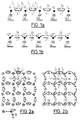
- FIG. 1a and 1b we have represented a one-dimensional network which includes a plurality of so-called horizontal capacities Cb and a plurality of so-called vertical capacities Cd.
- Cd capacity terminals are all connected to a potential of reference, in particular to mass.
- Each horizontal capacity Cb extends between the second terminals of two adjacent vertical capacitors.
- a plurality of two-position switches I are provided respectively between each terminal of a capacity horizontal Cb and each second adjacent terminal of a vertical capacity Cd.
- switches I can either take the position illustrated in Figure 1a, i.e. the position illustrated in Figure 1b.
- FIGS. 1a The behavior of the circuit of FIGS. 1a is as follows: at rest (FIG. 1a), the second terminals of the vertical capacitors Cd are isolated, and the voltages V 0 T to V N T are preserved.
- the switches I receive control voltages which place them in the position illustrated. In this position, short-circuiting links L provided in association with each horizontal capacity ensure complete discharge, by means of the two adjacent switches I, of said horizontal capacities.
- a control signal is applied simultaneously to the switches I to cause them to toggle in the position illustrated in FIG. 1b.
- the charges contained in the vertical capacities tend to balance, so that the voltages will diffuse in the network, according to an exponential law, towards the neighboring vertical capacities through the horizontal capacities, and the voltages V 0 T to V N T will vary gradually.
- the diffusion length of the voltages V 0 T to V N T is conditioned by the ratio between the values of the capacitances Cb and Cd, in a manner analogous to a resistive analog network.
- Equation (2) is an implicit approximation with finite difference from the heat equation (3a) in which the diffusion coefficient D would be equal to the ratio between the values of the capacities Cd and Cb.
- equation (2) above With finite difference, is absolutely stable, it is say that the truncation error tends to zero as the number of iterations increases.
- FIGS. 2a and 2b Illustrated in Figures 2a and 2b a network similar to that of Figures 1a and 1b, but two dimensions.
- equation (4) above is absolutely stable, i.e. the truncation error tends to zero as the number of iterations increases.
- figure 5 of the drawings shows in its part higher (curve (a)) the variance of the calculated response depending on the number of iterations, and in its part lower (curve (b)) the accumulated error between the calculated variance presented in curve (a) and the theoretical variance deduced from equation (4), after standardization.
- the first limit of the vertical capacity Cd is connected to ground, while its second terminal is connected on the one hand to the neighboring cell located immediately is via a MOS transistor Q1, and on the other hand to a first terminal of a parallel assembly with a horizontal capacitance Cb and another MOS transistor Q2.
- the second terminal of this parallel assembly is connected to the neighboring cell located immediately to the west.
- the gate of Q1 is connected to a bus carrying a control signal S1 consisting of a succession of determined frequency pulses.
- the grid for Q2 is connected to a bus carrying a S2 control signal constituted by a succession of pulses of the same frequency, interspersed in time between pulses of signal S1.
- a pulse is supplied by signal S2 to each transistor Q2, which saturates and short-circuits the terminals of the associated capacitor Cb, to completely discharge it.
- each transistor Q2 In the phase of diffusion of tensions, each transistor Q2 is blocked while each transistor Q1 is saturated for a certain period. We thus realize a charge transfer path between neighboring nodes via the capacitors Cb.
- the circuit of figure 4 illustrates the realization of a two-dimensional capacitive network in C-MOS technology.
- Each cell C (i, j) of the network includes a node N (i, j) of the network, and the associated vertical capacity Cd between this node and the mass.
- the node N (i, j) is also connected to the cell associated with node N (i, j + 1) located immediately south via the parallel mounting of a horizontal capacitance Cb and of a MOS transistor Q2, and the cell associated with node N (i-1, j) located immediately to the west via the parallel assembly another horizontal capacitance Cb and a MOS transistor Q2 '.
- the loading of the voltages initials to convolve on the different nodes of the network can be done by any switching technique classic.
- the collection of new tensions after iterations can be done by techniques of appropriate switching.
- the source of images consists of an array of photodiodes constituting a MOS imager.
- the vertical capacities Cd are replaced by the photodiodes themselves, the enough junction capacity for them to play, after exposure to photons, the same role as said vertical capacities.
- the noises of switching comes from crosstalk between signals, and raise particularly critical difficulties in the circuits where the output signals should be constantly sampled.
- the new knot tensions can be sampled by stopping the signals S1 and S2 clock. In other words, the phases iteration and sampling phases (application and voltage sampling) are done alternately. he there is therefore no annoying switching noise.
- Figure 6 illustrates the response of a prototype circuit produced according to the present invention.
- a 48x48 circuit pixels was produced in C-MOS technology, the sensors of light being produced in the form of C-MOS photodiodes integrated into the circuit.
- Original and after images convolutions were read with an analog scanner in current mode.
- a current-voltage converter connected to the output from the scanner converted the information to a analog voltage V applied to an oscilloscope, which has restored what is shown on figure 6.
- Figure 6 confirms the expected result, namely obtaining a quasi-Gaussian response as soon as the number of iterations becomes sufficient, with variance which is growing gradually.
- capacitive convolvers according to the present invention due to their recursion, avoid any aliasing phenomenon found in certain embodiments of the prior art and related to the use of a small convolution kernel dimensions.
- the present invention finds application in many areas such as image smoothing and noise elimination, edge detection and movements.
Landscapes
- Engineering & Computer Science (AREA)
- Physics & Mathematics (AREA)
- Theoretical Computer Science (AREA)
- Mathematical Physics (AREA)
- General Physics & Mathematics (AREA)
- Software Systems (AREA)
- Multimedia (AREA)
- Biomedical Technology (AREA)
- Computer Hardware Design (AREA)
- Biodiversity & Conservation Biology (AREA)
- Health & Medical Sciences (AREA)
- General Health & Medical Sciences (AREA)
- Molecular Biology (AREA)
- Computer Vision & Pattern Recognition (AREA)
- Life Sciences & Earth Sciences (AREA)
- Semiconductor Integrated Circuits (AREA)
- Solid State Image Pick-Up Elements (AREA)
- Transforming Light Signals Into Electric Signals (AREA)
- Analogue/Digital Conversion (AREA)
- Complex Calculations (AREA)
- Image Processing (AREA)
Description
- un réseau de premiers condensateurs, dont une première borne est reliée à un potentiel de référence commun et dont une seconde borne est apte à recevoir une tension électrique représentative d'un pixel d'image,
- un ensemble de seconds condensateurs respectivement associés à chaque paire adjacente, selon la ou les directions du réseau, de premiers condensateurs,
- des moyens interrupteurs commandés capables, pendant une première période prédéterminée, de connecter les bornes de chaque second condensateur aux secondes bornes de la paire associée de premiers condensateurs et, pendant une seconde période prédéterminée faisant suite à la première, d'isoler lesdites secondes bornes de la paire associée de premiers condensateurs et de court-circuiter ensemble les bornes de chaque second condensateur.
Claims (7)
- Procédé pour effectuer des opérations récursives de convolution notamment bidimensionnelle de type gaussien sur un ensemble de pixels d'une image, chaque pixel étant représenté par une tension électrique, caractérisé en ce qu'il comprend les étapes suivantes :a) on applique lesdites tensions électriques aux bornes d'une pluralité de premiers condensateurs (Cd) dont des premières bornes sont reliées à un potentiel de référence et dont des secondes bornes constituent une pluralité de noeuds (N(i,j)) d'un réseau et sont électriquement isolées les unes des autres,b) on connecte ensemble pendant une durée prédéterminée les noeuds immédiatement adjacents selon la ou les directions du réseau via des seconds condensateurs (Cb), non chargés,c) on isole à nouveau les uns des autres les noeuds du réseau et l'on décharge les seconds condensateurs,d) on réitère les étapes b) et c), ete) on relève les nouvelles tensions électriques présentes aux noeuds du réseau, représentatives des pixels d'une image convoluée.
- Procédé selon la revendication 1, caractérisé en ce que les étapes b) et c) sont effectuées en appliquant des impulsions de commande à des moyens de commutation (I) reliés d'une part aux bornes de chaque second condensateur (Cb) et d'autre part, sélectivement, soit à une seconde borne d'un premier condensateur associé (Cd), soit à une liaison de court-circuitage (L) associée au second condensateur considéré.
- Dispositif pour la mise en oeuvre du procédé selon la revendication 1, caractérisé en ce qu'il comprend, en combinaison :un réseau de premiers condensateurs (Cd), dont une première borne est reliée à un potentiel de référence commun et dont une seconde borne est apte à recevoir une tension électrique représentative d'un pixel d'image,un ensemble de seconds condensateurs (Cb) respectivement associés à chaque paire adjacente, selon la ou les directions du réseau, de premiers condensateurs,des moyens interrupteurs commandés (Q1, Q2; Q1, Q1', Q2, Q2') capables, pendant une première période prédéterminée, de connecter les bornes de chaque second condensateur (Cb) aux secondes bornes de la paire associée de premiers condensateurs (Cd) et, pendant une seconde période prédéterminée faisant suite à la première, d'isoler lesdites secondes bornes de la paire associée de premiers condensateurs et de court-circuiter ensemble les bornes de chaque second condensateur (Cb).
- Dispositif selon la revendication 3, caractérisé en ce que les premiers condensateurs sont constitués par la capacité de jonction de photodiodes, lesdites photodiodes étant aptes à engendrer lesdites tensions électriques représentatives des pixels d'image en réponse à la réception de photons constituant ladite image.
- Dispositif selon l'une des revendications 3 et 4, caractérisé en ce que les moyens interrupteurs commandés comprennent des premiers interrupteurs commmandés (Q1, Q1') reliés chacun en série avec un second condensateur associé et des seconds interrupteurs commandés (Q2, Q2') reliés chacun en parallèle avec un second condensateur associé.
- Dispositif selon la revendication 5, caractérisé en ce qu'il est prévu en outre des moyens générateurs d'impulsions pour engendrer des premières impulsions de fermeture des premiers interrupteurs (Q1, Q1') pendant lesdites premières périodes de temps et pour engendrer des secondes impulsions de fermeture des seconds interrupteurs (Q2, Q2') pendant lesdites secondes périodes de temps.
- Dispositif selon l'une des revendications 5 et 6, caractérisé en ce que les premiers et seconds condensateurs et les premiers et seconds interrupteurs sont réalisés en technologie C-MOS sur un même substrat semi-conducteur.
Applications Claiming Priority (2)
| Application Number | Priority Date | Filing Date | Title |
|---|---|---|---|
| FR9215093A FR2699307B1 (fr) | 1992-12-15 | 1992-12-15 | Procédé et dispositif pour la convolution analogique d'images. |
| FR9215093 | 1992-12-15 |
Publications (2)
| Publication Number | Publication Date |
|---|---|
| EP0603070A1 EP0603070A1 (fr) | 1994-06-22 |
| EP0603070B1 true EP0603070B1 (fr) | 1999-10-06 |
Family
ID=9436606
Family Applications (1)
| Application Number | Title | Priority Date | Filing Date |
|---|---|---|---|
| EP93403037A Expired - Lifetime EP0603070B1 (fr) | 1992-12-15 | 1993-12-15 | Procédé et dispositif pour la convolution analogique d'images |
Country Status (5)
| Country | Link |
|---|---|
| US (1) | US5521857A (fr) |
| EP (1) | EP0603070B1 (fr) |
| JP (1) | JP3479333B2 (fr) |
| DE (1) | DE69326674T2 (fr) |
| FR (1) | FR2699307B1 (fr) |
Families Citing this family (6)
| Publication number | Priority date | Publication date | Assignee | Title |
|---|---|---|---|---|
| FR2738933A1 (fr) * | 1995-09-19 | 1997-03-21 | Peugeot | Procede et dispositif pour extraire des points caracteristiques d'une image en niveaux de gris |
| US6111992A (en) * | 1997-07-28 | 2000-08-29 | Likhterov; Boris | Real-time two-dimensional filtering of video signals |
| US6198089B1 (en) * | 1999-03-31 | 2001-03-06 | The Hong Kong University Of Science And Technology | Steerable and scalable spatial filters |
| US9825132B2 (en) * | 2015-10-13 | 2017-11-21 | University Of Notre Dame Du Lac | Systems and methods for filtering and computation using tunneling transistors |
| CN111144558B (zh) * | 2020-04-03 | 2020-08-18 | 深圳市九天睿芯科技有限公司 | 基于时间可变的电流积分和电荷共享的多位卷积运算模组 |
| CN114757328B (zh) * | 2021-01-08 | 2025-10-21 | 中国科学院微电子研究所 | 一种卷积神经网络的卷积操作方法及装置 |
Family Cites Families (3)
| Publication number | Priority date | Publication date | Assignee | Title |
|---|---|---|---|---|
| US4555770A (en) * | 1983-10-13 | 1985-11-26 | The United States Of America As Represented By The Secretary Of The Air Force | Charge-coupled device Gaussian convolution method |
| US4956564A (en) * | 1989-07-13 | 1990-09-11 | Intel Corporation | Adaptive synapse cell providing both excitatory and inhibitory connections in an associative network |
| FR2656185B1 (fr) * | 1989-12-14 | 1992-03-13 | France Etat Armement | Imageur convolueur micro-electronique. |
-
1992
- 1992-12-15 FR FR9215093A patent/FR2699307B1/fr not_active Expired - Fee Related
-
1993
- 1993-12-14 US US08/166,650 patent/US5521857A/en not_active Expired - Lifetime
- 1993-12-15 EP EP93403037A patent/EP0603070B1/fr not_active Expired - Lifetime
- 1993-12-15 JP JP34315693A patent/JP3479333B2/ja not_active Expired - Fee Related
- 1993-12-15 DE DE69326674T patent/DE69326674T2/de not_active Expired - Lifetime
Also Published As
| Publication number | Publication date |
|---|---|
| FR2699307A1 (fr) | 1994-06-17 |
| JP3479333B2 (ja) | 2003-12-15 |
| US5521857A (en) | 1996-05-28 |
| DE69326674D1 (de) | 1999-11-11 |
| FR2699307B1 (fr) | 1995-03-03 |
| JPH06295349A (ja) | 1994-10-21 |
| DE69326674T2 (de) | 2000-04-27 |
| EP0603070A1 (fr) | 1994-06-22 |
Similar Documents
| Publication | Publication Date | Title |
|---|---|---|
| EP0237365B1 (fr) | Dispositif photosensible | |
| EP0143039B1 (fr) | Procédé de fabrication d'une matrice de composants électroniques | |
| EP0233104A1 (fr) | Matrice d'élements photosensibles et son procédé de fabrication, procédé de lecture associé, et application de cette matrice à la prise de vue d'images | |
| EP1646147B1 (fr) | Filtre analogique à composants passifs pour signaux à temps discret | |
| EP0783227A2 (fr) | Dispositif de lecture de barrettes de détecteurs avec effet TDI | |
| EP0245147A1 (fr) | Panneau de prise de vue radiologique, et procédé de fabrication | |
| FR2481553A1 (fr) | Dispositif photosensible lu par transfert de charges et camera de television comportant un tel dispositif | |
| FR2666714A1 (fr) | Detecteur d'image a pixels de grandes dimensions. | |
| EP0011556A1 (fr) | Filtre à transfert de charges électriques, programmable numériquement | |
| EP0082035B1 (fr) | Dispositif d'enregistrement et de lecture d'images | |
| EP0603070A1 (fr) | Procédé et dispositif pour la convolution analogique d'images | |
| EP0965224B1 (fr) | Procede de commande d'un dispositif photosensible a faible remanence, et dispositif photosensible mettant en oeuvre le procede | |
| EP0796006A1 (fr) | Procédé pour fournir une représentation d'une scène optique par transformation de Walsh-Hadamard et capteur d'image mettant en oeuvre ce procédé | |
| EP0012667B1 (fr) | Procédé de filtrage d'un signal électrique par transfert de charges dans un semi-conducteur et filtre à capacités commutées utilisant un tel procédé | |
| FR2508746A1 (fr) | Capteur d'image | |
| EP0129470B1 (fr) | Dispositif photosensible à l'état solide | |
| EP0938732B1 (fr) | Cellule electronique analogique, notamment destinee a etre implantee dans un circuit integre, et circuit integre comportant de telles cellules | |
| EP2486724B1 (fr) | Procédé pour la réduction du bruit dans le signal d'image d'un dispositif photosensible | |
| EP0917288B1 (fr) | Cellule comportant une pseudo-capacité notamment pour rétine artificielle | |
| EP0021908B1 (fr) | Dispositif inverseur de phase à transfert de charges et amplificateur différentiel comportant un tel dispositif | |
| EP0325524A1 (fr) | Mémoire à transfert de charges et procédé de fabrication de cette mémoire | |
| EP0143024B1 (fr) | Intégrateur exponentiel à constante de temp élevée, réalisé avec des capacités commutées | |
| EP1217629B1 (fr) | Procédé d'acquisition par échantillonnage de signaux analogiques et système d'acquisition pour la mise en oeuvre de ce procédé | |
| FR2656185A1 (fr) | Imageur convolueur micro-electronique. | |
| EP0275740B1 (fr) | Circuit de lecture d'un dispositif photosensible à transfert de ligne, dispositif photosensible à transfert de ligne comportant un tel circuit, et procédé de lecture d'un tel dispositif |
Legal Events
| Date | Code | Title | Description |
|---|---|---|---|
| PUAI | Public reference made under article 153(3) epc to a published international application that has entered the european phase |
Free format text: ORIGINAL CODE: 0009012 |
|
| AK | Designated contracting states |
Kind code of ref document: A1 Designated state(s): DE GB |
|
| 17P | Request for examination filed |
Effective date: 19941121 |
|
| GRAG | Despatch of communication of intention to grant |
Free format text: ORIGINAL CODE: EPIDOS AGRA |
|
| 17Q | First examination report despatched |
Effective date: 19981203 |
|
| RHK1 | Main classification (correction) |
Ipc: G06G 7/19 |
|
| GRAG | Despatch of communication of intention to grant |
Free format text: ORIGINAL CODE: EPIDOS AGRA |
|
| GRAH | Despatch of communication of intention to grant a patent |
Free format text: ORIGINAL CODE: EPIDOS IGRA |
|
| GRAH | Despatch of communication of intention to grant a patent |
Free format text: ORIGINAL CODE: EPIDOS IGRA |
|
| GRAA | (expected) grant |
Free format text: ORIGINAL CODE: 0009210 |
|
| AK | Designated contracting states |
Kind code of ref document: B1 Designated state(s): DE GB |
|
| RIC1 | Information provided on ipc code assigned before grant |
Free format text: 6G 06F 17/15 A, 6G 06G 7/19 B |
|
| REF | Corresponds to: |
Ref document number: 69326674 Country of ref document: DE Date of ref document: 19991111 |
|
| GBT | Gb: translation of ep patent filed (gb section 77(6)(a)/1977) |
Effective date: 19991119 |
|
| PLBE | No opposition filed within time limit |
Free format text: ORIGINAL CODE: 0009261 |
|
| STAA | Information on the status of an ep patent application or granted ep patent |
Free format text: STATUS: NO OPPOSITION FILED WITHIN TIME LIMIT |
|
| 26N | No opposition filed | ||
| REG | Reference to a national code |
Ref country code: GB Ref legal event code: IF02 |
|
| PGFP | Annual fee paid to national office [announced via postgrant information from national office to epo] |
Ref country code: GB Payment date: 20091125 Year of fee payment: 17 |
|
| PGFP | Annual fee paid to national office [announced via postgrant information from national office to epo] |
Ref country code: DE Payment date: 20091204 Year of fee payment: 17 |
|
| GBPC | Gb: european patent ceased through non-payment of renewal fee |
Effective date: 20101215 |
|
| PG25 | Lapsed in a contracting state [announced via postgrant information from national office to epo] |
Ref country code: DE Free format text: LAPSE BECAUSE OF NON-PAYMENT OF DUE FEES Effective date: 20110701 Ref country code: GB Free format text: LAPSE BECAUSE OF NON-PAYMENT OF DUE FEES Effective date: 20101215 |
|
| REG | Reference to a national code |
Ref country code: DE Ref legal event code: R119 Ref document number: 69326674 Country of ref document: DE Effective date: 20110701 |