EP0602852A2 - System and method for controlling voltages in a printing apparatus - Google Patents
System and method for controlling voltages in a printing apparatus Download PDFInfo
- Publication number
- EP0602852A2 EP0602852A2 EP93309683A EP93309683A EP0602852A2 EP 0602852 A2 EP0602852 A2 EP 0602852A2 EP 93309683 A EP93309683 A EP 93309683A EP 93309683 A EP93309683 A EP 93309683A EP 0602852 A2 EP0602852 A2 EP 0602852A2
- Authority
- EP
- European Patent Office
- Prior art keywords
- voltage
- substrate
- exposing
- radiation power
- substep
- Prior art date
- Legal status (The legal status is an assumption and is not a legal conclusion. Google has not performed a legal analysis and makes no representation as to the accuracy of the status listed.)
- Granted
Links
Images


Classifications
-
- H—ELECTRICITY
- H04—ELECTRIC COMMUNICATION TECHNIQUE
- H04N—PICTORIAL COMMUNICATION, e.g. TELEVISION
- H04N1/00—Scanning, transmission or reproduction of documents or the like, e.g. facsimile transmission; Details thereof
- H04N1/23—Reproducing arrangements
- H04N1/29—Reproducing arrangements involving production of an electrostatic intermediate picture
- H04N1/295—Circuits or arrangements for the control thereof, e.g. using a programmed control device, according to a measured quantity
-
- G—PHYSICS
- G03—PHOTOGRAPHY; CINEMATOGRAPHY; ANALOGOUS TECHNIQUES USING WAVES OTHER THAN OPTICAL WAVES; ELECTROGRAPHY; HOLOGRAPHY
- G03G—ELECTROGRAPHY; ELECTROPHOTOGRAPHY; MAGNETOGRAPHY
- G03G15/00—Apparatus for electrographic processes using a charge pattern
- G03G15/02—Apparatus for electrographic processes using a charge pattern for laying down a uniform charge, e.g. for sensitising; Corona discharge devices
- G03G15/0266—Arrangements for controlling the amount of charge
-
- G—PHYSICS
- G03—PHOTOGRAPHY; CINEMATOGRAPHY; ANALOGOUS TECHNIQUES USING WAVES OTHER THAN OPTICAL WAVES; ELECTROGRAPHY; HOLOGRAPHY
- G03G—ELECTROGRAPHY; ELECTROPHOTOGRAPHY; MAGNETOGRAPHY
- G03G15/00—Apparatus for electrographic processes using a charge pattern
- G03G15/02—Apparatus for electrographic processes using a charge pattern for laying down a uniform charge, e.g. for sensitising; Corona discharge devices
- G03G15/0291—Apparatus for electrographic processes using a charge pattern for laying down a uniform charge, e.g. for sensitising; Corona discharge devices corona discharge devices, e.g. wires, pointed electrodes, means for cleaning the corona discharge device
-
- G—PHYSICS
- G03—PHOTOGRAPHY; CINEMATOGRAPHY; ANALOGOUS TECHNIQUES USING WAVES OTHER THAN OPTICAL WAVES; ELECTROGRAPHY; HOLOGRAPHY
- G03G—ELECTROGRAPHY; ELECTROPHOTOGRAPHY; MAGNETOGRAPHY
- G03G15/00—Apparatus for electrographic processes using a charge pattern
- G03G15/04—Apparatus for electrographic processes using a charge pattern for exposing, i.e. imagewise exposure by optically projecting the original image on a photoconductive recording material
- G03G15/04036—Details of illuminating systems, e.g. lamps, reflectors
- G03G15/04045—Details of illuminating systems, e.g. lamps, reflectors for exposing image information provided otherwise than by directly projecting the original image onto the photoconductive recording material, e.g. digital copiers
Definitions
- This invention relates to system and method of controlling voltages in a printing apparatus, and more particularly to a system and method of controlling voltages in a printing apparatus employing a charged substrate and toner.
- halftone cells the image to be reproduced is partitioned into mutually exclusive areas called "halftone cells," each containing a number of pixels.
- halftone cells are used with a developable image printer, gray levels are simulated by exposing a subset of the total number of pixels in a halftone cell, to attract toner to the exposed pixels.
- the pixels are too small for a viewer to perceive individual pixels, and the viewer instead perceives a gray level corresponding to the percentage of halftone cell area that is covered with toner.
- Numerous physical conditions within the developable image printer affect various aspects of the appearance of a halftone cell. A variation in a single physical condition may cause a variation in multiple aspects a cell's appearance.
- the present invention provides a method of operating a reproduction system including a substrate and means for depositing toner onto the substrate, comprising the steps of receiving a first number N1; receiving a second number N2; receiving a third number N3; charging the depositing means to a first voltage; charging the substrate to produce a second voltage, such that a difference between the second voltage and the first voltage is N1; discharging selected areas of the substrate to produce a third voltage, such that a difference between the third voltage and the first voltage is N2, and a ratio between a function of the second voltage and a function of the third voltage is N3.
- the invention further provides a printing apparatus according to claim 10 of the appended claims.
- Fig. 1 is a diagram of a printing apparatus of a first embodiment of the invention.
- Fig. 2 is a diagram of a halftone cell.
- Fig. 3 is a diagram of another halftone cell.
- Fig. 4 is diagram of the controller for the printing apparatus of Fig. 1.
- Fig. 5 is a graph illustrating voltages employed by the printing system of Fig. 1.
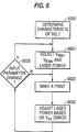
- Fig. 6 is a flow diagram showing an operation of the first embodiment of the present invention.
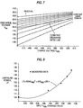
- Fig. 7 is a graph showing data acquired by the printing apparatus of Fig. 1.
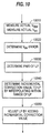
- Fig. 8 is a flow diagram showing the process of Fig. 6 in more detail.
- Fig. 9 is a graph showing a relationship between substrate charge voltage and laser exposure power in the printer apparatus of Fig. 1.
- Fig. 10 is a flow diagram showing the process of Fig. 6 in more detail.
- Fig. 11 is a graph showing a step input response of the printer of Fig. 1.
- Fig. 12 is a graph showing an effect of the printing apparatus of Fig. 1.
- Fig. 13 is a diagram of a printing apparatus of a second embodiment of the invention.
- Fig. 14 is a diagram of a printing apparatus of a third embodiment of the invention.
- Fig. 15 is a diagram of another halftone cell.
- Fig. 1 shows a printing apparatus 1000 of a first embodiment of the present invention.
- Photoreceptor belt 1010 is entrained around rollers 1014.
- rollers 1014 is rotated by a motor (not shown) via by suitable means such as a belt drive.
- suitable means such as a belt drive.
- the driven roller advances belt 1010 in the direction of arrow 1012 through the various processing stations disposed around the movement path of belt 1010.
- Corotrons 1022 and 1024 operate to charge belt 1010 to a uniform potential.
- Raster scanning laser 1032 exposes belt 1010 to a pattern of light to render a latent image.
- Developing station 1037 deposits toner on belt 1010.
- Bias voltage source 1100 charges developing station 1037.
- Charge sensor 1115 senses a charge on belt 1010.
- Controller 1500 controls voltages in the preferred printer, as described in detail later.
- the area of the belt 1010 is exposed to a pretransfer light from a lamp (not shown) to reduce the attraction between belt 1010 and the toner deposited by developer 1037.
- a corotron 1046 charges a sheet of paper, from paper tray 1082, to an appropriate magnitude so that the paper is tacked to belt 1010 and the toner attracted from belt 1010 to the paper.
- detack corotron 1048 charges the paper to an opposite polarity to detack the paper from belt 1010.
- the paper then passes to fuser 1052 where the toner is fused into the paper with heat and pressure.
- the paper then advances to output section 1190, or to tray 1066 allowing the paper to return to belt 1010 for printing an image on an opposite side of the paper.
- Fig. 2 shows a highly magnified halftone cell 2000 having 9 pixels 2010-2090.
- laser 1032 exposes none of the pixels in the cell resulting in the cell shown in Fig. 2.
- laser 1032 exposes some of the pixels in the cell to attract toner to the exposed pixels.
- laser 1032 exposes all pixels in the cell to attract toner to the exposed pixels.
- the combination of voltages employed within printer 1000 has an effect on the production of intermediate levels of gray. This effect results from certain phenomena that occur at an interface between an exposed pixel and an unexposed pixel. Depending on the combination of voltages, an unexposed pixel may contain various amounts of toner in an area near an interface with an exposed pixel, thereby affecting the perceived gray level.
- Fig. 3 shows a highly magnified halftone cell in which laser 1032 has exposed 3 of the 9 pixels to produce an intermediate gray level.
- Laser 1032 has exposed pixels 3010, 3020 and 3050 to attract toner to these exposed pixels.
- unexposed pixels 3040, 3070, 3080, 3090, 3060 and 3030 contain toner resulting from the exposure of pixels 3010, 3020 and 3050.
- Controller 1500 includes a general purpose computer executing a controller program. Controller 1500 controls a charge on belt 1010 by controlling corotrons 1022 and 1024 in accordance with a parameter V ddp , described below. Controller 1500 also controls a power of laser 1032 in accordance with a parameter LP, and controls bias voltage source 1100 in accordance with a parameter V bias , described below. Controller 1500 receives input parameters V clean , V dev and DR described below, and an output of charge sensor 1115.
- the parameter V clean received by controller 1500 controls a voltage difference between belt 1010, after charging by corotrons 1022 and 1024, and the rollers in developer 1037.
- An electric field produced by this voltage difference is sometimes called the "cleaning field," because this electric field tends to suppress the deposition of background toner on white pixels, such as pixel 2090 in Fig. 2.
- Printer 1000 initially sets V clean to 100 volts to suppress the deposition of background while providing adequate reproduction of grey levels close to white.
- the parameter V dev received by controller 1500 controls a voltage difference between belt 1010, after exposure by laser 1032, and the rollers in developer 1037.
- An electric field produced by this voltage difference is sometimes called the "development field," because this electric field tends to promote the deposition of toner on exposed pixels.
- V rsl is a residual voltage obtained when the photoreceptor is maximally discharged by light. V rsl is reached when additional exposure power increases cause negligible additional voltage discharge.
- the parameter DR received by controller 1500 specifies the discharge ratio in printer 1000.
- the discharge ratio is a factor determining the amount of toner deposited near an edge in an unexposed pixels, such as pixel 3030 in Fig. 3, resulting from exposure of an adjacent pixel, such as pixel 3020.
- Printer 1000 initially sets DR to 0.1 to produce an amount of toner in a cell that is a roughly linear function of the percentage of exposed pixels in the cell.
- FIG. 5 shows voltages employed by printer 1000 to achieve latent image formation.
- An electrostatic voltmeter placed 1.2 seconds after charging would measure the indicated V ddp and V ex .
- V rsl is a physical characteristic of the particular materials used for belt 1010.
- V rsl is measured by controller 1500, as described later.
- the discharge ratio may be conceptualized as corresponding t the location of a range, defined by V clean and V dev , relative to the V rsl . In Fig. 5, the discharge ratio is approximately 0.16.
- Fig. 6 shows a processing of controller 1500 to set a belt charge V ddp , a laser power LP and a V bias in response to the received input parameters V clean , V dev , and DR. Certain characteristics of belt 1010 are determined (step 6002). Step 6002 is preferably performed upon the power-up of printer 1000, before images on paper are produced.
- Fig. 7 shows data acquired by controller 1500 in step 6002.
- a matrix is developed by performing measurements at different values of V ddp and V ex .
- Each of the 10 curves of Fig. 7 represents data collected at a certain constant exposure power of laser 1032.
- V ex V ex .
- Controller 1500 uses the data of Fig 7 to set a laser 1032 exposure power LP to achieve the V ex that results in the specified V dev , V clean and DR. Controller 1500 effectively constrains V ex to be on the line of constant DR, relative to the residual curve, shown in Fig. 7. This line of constant DR correlates V ex values with V ddp values. Each intersection point of the line of constant DR with any of the 10 curves of constant exposure power gives a guide to the appropriate laser 1032 exposure power LP for a given V ddp . For each intersection a pair of power, charge values is obtained.
- Controller 1500 calculates a new line of constant discharge ratio each time step 6004 is performed.
- the printing apparatus makes prints (Step 6020), and adjusts laser power (Step 6030). If one or more of the input parameters V clean , V dev or DR change (step 6035), controller 1500 performs step 6004 again.
- Laser 1032 is configured as a raster output scanner (ROS) capable of varying exposure power quickly to a number of values in the time that it would normally take to print an image.
- the data shown in Fig. 7 is the V ex result of 10 exposure powers measured at each of 16 V ddp levels in 16 passes of the photoreceptor, one pass for each V ddp level.
- the top curve in Fig. 7 corresponds a laser power that discharges belt 1010 to a residual voltage meaning that higher laser powers do not cause further discharge of belt 1010 within the exposure time of laser 1032.
- the top curve corresponds to laser powers that result in the residual voltage V rsl .
- This residual voltage is somewhat dependent on V ddp , an embellishment on the equations above that will be described later.
- Fig. 8 shows a processing of step 6002 of Fig. 6 in more detail.
- Fig. 8 shows a processing of controller 1500 to collect the data shown in Fig. 7.
- Initial substrate charge and laser powers are selected (Steps 8010 and 8020). The substrate is exposed with the currently selected laser power and the resulting discharged voltage measured by charge sensor 1115 V ex is stored. If laser powers remain (Step 8040), a next laser power is selected (Step 8050) and a new exposed and measuring step is performed. If no laser powers remain, it is determined whether any values for V ddp remain (Step 8060) and if other values of V ddp remain a new value for V ddp is set (Step 8070) and control returns to Step 8020.
- controller 1500 performs the steps of charging the substrate to each of a plurality of predetermined voltages; exposing, for each predetermined voltage, the substrate to each of a plurality of predetermined radiation powers; measuring, for each radiation power, a charge on the substrate after the exposing step; and determining a radiation power by using a result of the measuring step to interpolate between two of the plurality of predetermined radiation powers.
- printer 1000 exposes belt 1010 with the determined radiation power.
- V ex there will be error in V ex which may result from changes in the photoreceptor characteristics with age or environment that have occurred since step 6002 was performed.
- Another error source is small deviations of real photoreceptor behavior from the behavior predicted by the mathematical curve fit described above.
- An error feedback calculation adjusts the exposure power to minimize V ex error and compensate for these errors.
- an imaginary vertical line at the measured V ddp can be drawn. This line also intersects the lines of constant laser power and each intersection can be used to create LP, V ex pairs.
- a functional fit using V ex as the independent variable allows a power correction to be calculated that will return V ex to zero error. This power correction value is adjusted on each revolution of belt 1010 in accordance with the measured error.
- Printer 1000 may be configured with a wide variety of photoreceptors and exposure sources.
- a preferred embodiment of the invention configures printer 1000 with an organic infrared sensitive photoreceptor exposed by an infrared laser diode source.
- V ex is substantially a linear function of V ddp at constant laser power.
- V rsl a0(v ddp ) + b0
- V ex V ddp [DR(1-a0) + a0] + b0(1-DR)
- V ddp ,i [b i - b0(1-DR)]/[a0 - a i + DR(1-a0)] - over all LP
- Fig. 9 shows a relationship between V ddp and laser power LP for a particular DR.
- V ddp pairs substantially fit to a quadratic equation, as shown in Fig. 9.
- the intersection points as seen in Fig. 7 are used to generate 5 pairs of LP, V ddp .
- a parabola is fitted to these 5 pairs of values.
- the coefficients of the fitted curve are used to calculate an initial LP from V ddp .
- the functional values diverge slightly at high charges, which is inconsistent with the actual data. This divergence is an artifact of the fitting equation and can introduce an error in the initial setting of LP by controller 1500.
- Controller 1500 employs feedback to readjust the setting of LP, thereby compensating for the error introduced by the divergence and for error introduced by physical changes occurring after the initial setting of LP.
- Fig. 10 shows a processing of step 6030 of Fig. 6 in more detail
- Charge sensor 1115 measures an actual V ddp , and an actual V ex (Step 10010).
- the measured V ddp is used to determine a target V ex to achieve the discharge ratio DR, thereby determining a (Step 10020).
- a pair of laser powers that yield V ex values that include the actual V ex at the actual V ddp is determined (Step 10030).
- V ex,i a i Z + b i for all LP l
- the preferred method includes the step of exposing the substrate to the determined radiation power; a second measuring step of measuring a voltage on the substrate after the exposing step; and redetermining a radiation power in accordance with the second measuring step.
- the redetermining of the radiation power compensates for the changes and maintains a low V ex error.
- Fig. 11 shows a response of controller 1500 to a step change at the DR input.
- the discharge ratio computed from measurements taken at an electrostatic voltmeter is plotted along with the DR input to controller 1500.
- the DR input was changed in the middle of a 32 print run. Also shown is the V ex error in volts, which indicates that there was a period of approximately three prints at the start of the run were the results of steps 10010-10050 converged to achieve substantially zero V ex error.
- controller 1500 used the data of Fig. 7 to follow the DR input. Small variations in V ex error are evident as the feedback control processing of steps 10010-10050 adjusted to the new DR input.
- Fig. 12 shows three curves relating a percentage of pixels exposed in a cell, on the horizontal axis, with an amount of toner deposited in the cell, on the vertical axis. These three curves were each produced by a 5th order polynomial fit to experimental data. Comparing the two curves of constant Vclean and changing DR shows that the effect of a change in DR is to alter the middle of the curve while leaving the endpoints unchanged. In contrast, a change in V clean at a constant DR affects mainly the highlight end of the curve, thereby demonstrating that controller 1500 can control the curve shape substantially independently of black level optical density.
- Printer 1000 may adjust DR to maintain a 50% halftone dot density, and may adjust V dev to maintain solid area tone density. Printer 1000 might also adjust V clean to maintain a certain suppression of background. Printer 1000 may perform automatic adjustment of these parameters in response to physical changes in printer 1000 caused by, for example, a change in room humidity. Printer 1000 may perform automatic adjustment of these parameters by exposing test patches of the belt 1010 with laser 1032 and developing the test patches with developer 1037. Subsequently, an amount of toner on the test patches is measured. The test patches are on an interdocument gap on belt 1010 so that the normal printing of paper is not adversely affected by the adjustment process.
- Fig. 13 shows a schematic diagram of a printing apparatus of a second embodiment of the present invention, including a visible light sensitive inorganic photoreceptor 13020, charge corotron 13022, laser 13032, mirror 13034, and controller 13500.
- a first electrostatic volt meter (ESV1) 13040 opposes photoreceptor 13020 at a location 0.176 seconds downstream from a reference location.
- Cyan developer 13045 is located 0.407 seconds downstream from the reference location
- second electrostatic voltmeter (ESV2) 13050 is located 0.622 downstream form the reference location
- yellow developer 13055 is located 0.792 seconds downstream from the reference location
- magenta developer 13060 is located 1.073 seconds downstream from the reference location
- black developer 13065 is located 1.361 seconds downstream from the reference location
- pre-transfer electrostatic voltmeter 13070 is located at 1.549 seconds downstream from the reference location.
- Optimized color densitometer 13075 is located adjacent pre-transfer electrostatic voltmeter 13070.
- photoreceptor 13020 is rotated four times, one time for each color, and a single copy sheet is brought into contact with photoreceptor 13020 four times. On each rotation, only one of cyan developer 13045, yellow developer 13055, magenta developer 13060, or black developer 13065 is activated.
- ESV2 13050 allows for a prediction of charge decay, by taking a measurement that is compared to a measurement taken by ESV1 13040.
- Controller 13500 includes four independent subcontrollers, one for each color. Each subcontroller uses a common set of set photoreceptor characterization data, such as the data shown in Fig. 7. Each subcontroller has a respective constant discharge ratio line, since each color may have a different DR set point. Each color will also have a different charge voltage V ddp at the measurement point of electrostatic voltmeter 13050.
- Fig. 14 shows a printing apparatus of a third embodiment of the present invention, including a raster input section 14015, and image processing section 14017, a raster output section 14032, which includes a laser, a mirror 14034, a photoreceptor 14010, a corotron 14022, and electrostatic voltmeter 14050, developer 14045, developer 14055, developer 14060, developer 14065, a paper tray 14082, an output section 14190, and a controller 14500.
- a raster input section 14015 and image processing section 14017
- a raster output section 14032 which includes a laser, a mirror 14034, a photoreceptor 14010, a corotron 14022, and electrostatic voltmeter 14050, developer 14045, developer 14055, developer 14060, developer 14065, a paper tray 14082, an output section 14190, and a controller 14500.
- the preferred embodiments of the present invention provide a method to adjust voltages to allow relatively independent control of toner quantities for black, white, and intermediate density level cells.
- a controller translates three xerographic parameters, V dev , V clean , and DR, into appropriate control of the physical xerographic elements of a photoreceptor charging device, developer bias and laser exposure intensity.
- the DR parameter controls the optical density of intermediate grey levels, without substantial secondary effects on solid area density or background toner deposition.
- the charging level should be altered for any reason, such as an alteration of V dev or V clean , the exposure intensity is correspondingly altered to maintain DR.
- This independent control facilitates automation of the printing process, allowing print quality to remain constant when factors such as room humidity vary.
- Fig. 15 shows an alternative half-tone cell arrangement including 36 pixels per cell. Other cell arrangements are possible, including cell arrangements having more than 100 pixels per cell.
Abstract
Description
- This invention relates to system and method of controlling voltages in a printing apparatus, and more particularly to a system and method of controlling voltages in a printing apparatus employing a charged substrate and toner.
- In a certain printing method, the image to be reproduced is partitioned into mutually exclusive areas called "halftone cells," each containing a number of pixels. When halftone cells are used with a developable image printer, gray levels are simulated by exposing a subset of the total number of pixels in a halftone cell, to attract toner to the exposed pixels. The pixels are too small for a viewer to perceive individual pixels, and the viewer instead perceives a gray level corresponding to the percentage of halftone cell area that is covered with toner.
- Numerous physical conditions within the developable image printer affect various aspects of the appearance of a halftone cell. A variation in a single physical condition may cause a variation in multiple aspects a cell's appearance.
- It is an object of the present invention to control voltages within a printing apparatus to substantially control a single aspect of the appearance of a multipixel cell.
- To achieve this and other advantages of the invention the present invention provides a method of operating a reproduction system including a substrate and means for depositing toner onto the substrate, comprising the steps of receiving a first number N1; receiving a second number N2; receiving a third number N3; charging the depositing means to a first voltage; charging the substrate to produce a second voltage, such that a difference between the second voltage and the first voltage is N1; discharging selected areas of the substrate to produce a third voltage, such that a difference between the third voltage and the first voltage is N2, and a ratio between a function of the second voltage and a function of the third voltage is N3.
- The invention further provides a printing apparatus according to
claim 10 of the appended claims. - The accompanying drawings, which are incorporated in and which constitute a part of this specification, illustrate preferred embodiments of the invention and, together with the description, explain the principles of the invention.
- Fig. 1 is a diagram of a printing apparatus of a first embodiment of the invention.
- Fig. 2 is a diagram of a halftone cell.
- Fig. 3 is a diagram of another halftone cell.
- Fig. 4 is diagram of the controller for the printing apparatus of Fig. 1.
- Fig. 5 is a graph illustrating voltages employed by the printing system of Fig. 1.
- Fig. 6 is a flow diagram showing an operation of the first embodiment of the present invention.
- Fig. 7 is a graph showing data acquired by the printing apparatus of Fig. 1.
- Fig. 8 is a flow diagram showing the process of Fig. 6 in more detail.
- Fig. 9 is a graph showing a relationship between substrate charge voltage and laser exposure power in the printer apparatus of Fig. 1.
- Fig. 10 is a flow diagram showing the process of Fig. 6 in more detail.
- Fig. 11 is a graph showing a step input response of the printer of Fig. 1.
- Fig. 12 is a graph showing an effect of the printing apparatus of Fig. 1.
- Fig. 13 is a diagram of a printing apparatus of a second embodiment of the invention.
- Fig. 14 is a diagram of a printing apparatus of a third embodiment of the invention.
- Fig. 15 is a diagram of another halftone cell.
- Fig. 1 shows a
printing apparatus 1000 of a first embodiment of the present invention.Photoreceptor belt 1010 is entrained aroundrollers 1014. One or more ofrollers 1014 is rotated by a motor (not shown) via by suitable means such as a belt drive. As the driven roller rotates, the drivenroller advances belt 1010 in the direction ofarrow 1012 through the various processing stations disposed around the movement path ofbelt 1010. - Corotrons 1022 and 1024 operate to
charge belt 1010 to a uniform potential.Raster scanning laser 1032 exposesbelt 1010 to a pattern of light to render a latent image. Developingstation 1037 deposits toner onbelt 1010.Bias voltage source 1100charges developing station 1037.Charge sensor 1115 senses a charge onbelt 1010.Controller 1500 controls voltages in the preferred printer, as described in detail later. - After passing
developer 1037, the area of thebelt 1010 is exposed to a pretransfer light from a lamp (not shown) to reduce the attraction betweenbelt 1010 and the toner deposited bydeveloper 1037. A corotron 1046 charges a sheet of paper, frompaper tray 1082, to an appropriate magnitude so that the paper is tacked to belt 1010 and the toner attracted frombelt 1010 to the paper. Subsequently,detack corotron 1048 charges the paper to an opposite polarity to detack the paper frombelt 1010. The paper then passes tofuser 1052 where the toner is fused into the paper with heat and pressure. The paper then advances to outputsection 1190, or to tray 1066 allowing the paper to return tobelt 1010 for printing an image on an opposite side of the paper. - Fig. 2 shows a highly
magnified halftone cell 2000 having 9 pixels 2010-2090. To print white,laser 1032 exposes none of the pixels in the cell resulting in the cell shown in Fig. 2. To simulate an intermediate level of gray for the printing of a certain cell,laser 1032 exposes some of the pixels in the cell to attract toner to the exposed pixels. To print black,laser 1032 exposes all pixels in the cell to attract toner to the exposed pixels. - The combination of voltages employed within
printer 1000 has an effect on the production of intermediate levels of gray. This effect results from certain phenomena that occur at an interface between an exposed pixel and an unexposed pixel. Depending on the combination of voltages, an unexposed pixel may contain various amounts of toner in an area near an interface with an exposed pixel, thereby affecting the perceived gray level. - Fig. 3 shows a highly magnified halftone cell in which
laser 1032 has exposed 3 of the 9 pixels to produce an intermediate gray level. Laser 1032 has exposedpixels unexposed pixels pixels - Fig. 4 shows
controller 1500 forprinter 1000 the preferred printing apparatus.Controller 1500 includes a general purpose computer executing a controller program.Controller 1500 controls a charge onbelt 1010 by controllingcorotrons Controller 1500 also controls a power oflaser 1032 in accordance with a parameter LP, and controlsbias voltage source 1100 in accordance with a parameter Vbias, described below.Controller 1500 receives input parameters Vclean, Vdev and DR described below, and an output ofcharge sensor 1115. - The parameter Vclean received by
controller 1500 controls a voltage difference betweenbelt 1010, after charging bycorotrons developer 1037. An electric field produced by this voltage difference is sometimes called the "cleaning field," because this electric field tends to suppress the deposition of background toner on white pixels, such aspixel 2090 in Fig. 2.Printer 1000 initially sets Vclean to 100 volts to suppress the deposition of background while providing adequate reproduction of grey levels close to white. - The parameter Vdev received by
controller 1500 controls a voltage difference betweenbelt 1010, after exposure bylaser 1032, and the rollers indeveloper 1037. An electric field produced by this voltage difference is sometimes called the "development field," because this electric field tends to promote the deposition of toner on exposed pixels.Printer 1000 initially sets Vdev to 250 volts to obtain a density of 1.8 density units in black pixels, such aspixel 3020 in Fig. 3, where a density unit is -log (reflection ratio) = -log (sample reflectance) ÷ (reference light reflectance). - The preferred embodiment of the present invention employs a discharge ratio DR defined as:

where Vddp is a charge onbelt 1010 at a point downstream fromcorotrons belt 1010 that has been exposed bylaser 1032. Vrsl is a residual voltage obtained when the photoreceptor is maximally discharged by light. Vrsl is reached when additional exposure power increases cause negligible additional voltage discharge. - The parameter DR received by
controller 1500 specifies the discharge ratio inprinter 1000. The discharge ratio is a factor determining the amount of toner deposited near an edge in an unexposed pixels, such aspixel 3030 in Fig. 3, resulting from exposure of an adjacent pixel, such aspixel 3020.Printer 1000 initially sets DR to 0.1 to produce an amount of toner in a cell that is a roughly linear function of the percentage of exposed pixels in the cell. - Fig. 5 shows voltages employed by
printer 1000 to achieve latent image formation. An electrostatic voltmeter placed 1.2 seconds after charging would measure the indicated Vddp and Vex . Vrsl is a physical characteristic of the particular materials used forbelt 1010. Vrsl is measured bycontroller 1500, as described later. - The discharge ratio may be conceptualized as corresponding t the location of a range, defined by Vclean and Vdev, relative to the Vrsl. In Fig. 5, the discharge ratio is approximately 0.16.
- Fig. 6 shows a processing of
controller 1500 to set a belt charge Vddp, a laser power LP and a Vbias in response to the received input parameters Vclean, Vdev, and DR. Certain characteristics ofbelt 1010 are determined (step 6002).Step 6002 is preferably performed upon the power-up ofprinter 1000, before images on paper are produced. - Fig. 7 shows data acquired by
controller 1500 instep 6002. A matrix is developed by performing measurements at different values of Vddp and Vex. Each of the 10 curves of Fig. 7 represents data collected at a certain constant exposure power oflaser 1032. - The sixteen points that each curve follows are the measured Vex at 16 different Vddp levels. Also shown is the line of constant discharge ratio DR.
- A Vddp, Vbias and LP are selected based on the input parameters and on characteristics of
belt 1010 determined in step 6002 (step 6004 in Fig. 6). More specifically, the following equations determine Vddp, Vbias and Vex:

Using the formula for DR to solve for Vex, Vddp is:
and Vbias is:
- The Vex required to meet the Vdev, Vclean and DR specification is:

-
Controller 1500 uses the data of Fig 7 to set alaser 1032 exposure power LP to achieve the Vex that results in the specified Vdev, Vclean and DR.Controller 1500 effectively constrains Vex to be on the line of constant DR, relative to the residual curve, shown in Fig. 7. This line of constant DR correlates Vex values with Vddp values. Each intersection point of the line of constant DR with any of the 10 curves of constant exposure power gives a guide to theappropriate laser 1032 exposure power LP for a given Vddp. For each intersection a pair of power, charge values is obtained. A mathematical curve fit of these two variables, using charge as the independent variable, yields a function that converts Vddp (charge) into a laser power that produces a Vex consistent with the DR value (step 6004).Controller 1500 calculates a new line of constant discharge ratio eachtime step 6004 is performed. - Subsequently, the printing apparatus makes prints (Step 6020), and adjusts laser power (Step 6030). If one or more of the input parameters Vclean, Vdev or DR change (step 6035),
controller 1500 performsstep 6004 again. -
Laser 1032 is configured as a raster output scanner (ROS) capable of varying exposure power quickly to a number of values in the time that it would normally take to print an image. The data shown in Fig. 7 is the Vex result of 10 exposure powers measured at each of 16 Vddp levels in 16 passes of the photoreceptor, one pass for each Vddp level. - The top curve in Fig. 7 corresponds a laser power that discharges
belt 1010 to a residual voltage meaning that higher laser powers do not cause further discharge ofbelt 1010 within the exposure time oflaser 1032. In other words, the top curve corresponds to laser powers that result in the residual voltage Vrsl. This residual voltage is somewhat dependent on Vddp, an embellishment on the equations above that will be described later. - Fig. 8 shows a processing of
step 6002 of Fig. 6 in more detail. Fig. 8 shows a processing ofcontroller 1500 to collect the data shown in Fig. 7. Initial substrate charge and laser powers are selected (Steps 8010 and 8020). The substrate is exposed with the currently selected laser power and the resulting discharged voltage measured by charge sensor 1115 Vex is stored. If laser powers remain (Step 8040), a next laser power is selected (Step 8050) and a new exposed and measuring step is performed. If no laser powers remain, it is determined whether any values for Vddp remain (Step 8060) and if other values of Vddp remain a new value for Vddp is set (Step 8070) and control returns to Step 8020. - In other words,
controller 1500 performs the steps of charging the substrate to each of a plurality of predetermined voltages; exposing, for each predetermined voltage, the substrate to each of a plurality of predetermined radiation powers; measuring, for each radiation power, a charge on the substrate after the exposing step; and determining a radiation power by using a result of the measuring step to interpolate between two of the plurality of predetermined radiation powers. During printing,printer 1000 exposesbelt 1010 with the determined radiation power. - In general, there will be error in Vex which may result from changes in the photoreceptor characteristics with age or environment that have occurred since
step 6002 was performed. Another error source is small deviations of real photoreceptor behavior from the behavior predicted by the mathematical curve fit described above. An error feedback calculation adjusts the exposure power to minimize Vex error and compensate for these errors. In Fig. 7, an imaginary vertical line at the measured Vddp can be drawn. This line also intersects the lines of constant laser power and each intersection can be used to create LP, Vex pairs. A functional fit using Vex as the independent variable allows a power correction to be calculated that will return Vex to zero error. This power correction value is adjusted on each revolution ofbelt 1010 in accordance with the measured error. -
Printer 1000 may be configured with a wide variety of photoreceptors and exposure sources. A preferred embodiment of the invention configuresprinter 1000 with an organic infrared sensitive photoreceptor exposed by an infrared laser diode source. - The data in the graph of Fig. 7 was acquired from the organic infrared sensitive photoreceptor. In this case, Vex is substantially a linear function of Vddp at constant laser power. This set of lines at various powers can be expressed as:

- In an alternative embodiment employing inorganic visible light sensitive photoreceptor and a HeNe laser, the above relation was found to be quadratic.
- To determine an equation for the line of constant discharge ratio, the dependence of the residual voltage Vrsl on Vddp is determined. For both the inorganic visible light sensitive and organic infrared sensitive photoreceptors, a linear relation is adequate to calculate Vrsl from Vddp:

- From this relation and the definition of DR, the equation for the line of constant discharge ratio is:

- Next the intersection points of the constant discharge ratio line and the sets for constant laser power are used to determine LP, Vddp data pairs:

Fig. 9 shows a relationship between Vddp and laser power LP for a particular DR. For organic infrared sensitive photoreceptor the LP, Vddp pairs substantially fit to a quadratic equation, as shown in Fig. 9. The intersection points as seen in Fig. 7 are used to generate 5 pairs of LP, Vddp. A parabola is fitted to these 5 pairs of values. The coefficients of the fitted curve are used to calculate an initial LP from Vddp. In Fig. 9, the functional values diverge slightly at high charges, which is inconsistent with the actual data. This divergence is an artifact of the fitting equation and can introduce an error in the initial setting of LP bycontroller 1500.Controller 1500 employs feedback to readjust the setting of LP, thereby compensating for the error introduced by the divergence and for error introduced by physical changes occurring after the initial setting of LP. - Thus, for an organic infrared sensitive photoreceptor, the initial exposure power LP is:

where the q coefficients describe the parabolic section in Fig. 9. - The analogous relation for an alternative embodiment employing inorganic visible light sensitive photoreceptor is a substantially linear function of Vddp.
- Fig. 10 shows a processing of
step 6030 of Fig. 6 in moredetail Charge sensor 1115 measures an actual Vddp, and an actual Vex (Step 10010). The measured Vddp is used to determine a target Vex to achieve the discharge ratio DR, thereby determining a (Step 10020). A pair of laser powers that yield Vex values that include the actual Vex at the actual Vddp is determined (Step 10030). - In other words, to determine the feedback power correction, the data of Fig. 7 is used again. Assuming that on the present belt revolution the Vddp measured by
charge sensor 1115 is Z volts, and according to the equations describing Vex as a function of Vddp at constant laser powers, a set of LP, Vex pairs is:
Two pairs are chosen having Vex values that bracket the actual Vex measured on this pass. - An incremental correction to the laser power is determined (Step 10040), and the laser power is adjusted using the determined incremental correction value (Step 10050). More specifically, ΔLP/ΔVex slope, defined by the two pairs, is calculated and multiplied by the Vex error (Vex_error) to obtain an LP correction. The LP correction value is subtracted from the current LP value:

- An alternative approach would be to perform a complete mathematical fit of the LP, Vex pairs.
- In other words, in addition to measuring a substrate voltage to collect the data of Fig. 7 and determining a radiation power based on the data of Fig. 7, the preferred method includes the step of exposing the substrate to the determined radiation power; a second measuring step of measuring a voltage on the substrate after the exposing step; and redetermining a radiation power in accordance with the second measuring step.
- As printing proceeds and the photoreceptor susceptibility to exposure changes, the redetermining of the radiation power compensates for the changes and maintains a low Vex error.
- Fig. 11 shows a response of
controller 1500 to a step change at the DR input. The discharge ratio computed from measurements taken at an electrostatic voltmeter is plotted along with the DR input tocontroller 1500. The DR input was changed in the middle of a 32 print run. Also shown is the Vex error in volts, which indicates that there was a period of approximately three prints at the start of the run were the results of steps 10010-10050 converged to achieve substantially zero Vex error. At the sixteenth print, when the DR input changes,controller 1500 used the data of Fig. 7 to follow the DR input. Small variations in Vex error are evident as the feedback control processing of steps 10010-10050 adjusted to the new DR input. - Fig. 12 shows three curves relating a percentage of pixels exposed in a cell, on the horizontal axis, with an amount of toner deposited in the cell, on the vertical axis. These three curves were each produced by a 5th order polynomial fit to experimental data. Comparing the two curves of constant Vclean and changing DR shows that the effect of a change in DR is to alter the middle of the curve while leaving the endpoints unchanged. In contrast, a change in Vclean at a constant DR affects mainly the highlight end of the curve, thereby demonstrating that
controller 1500 can control the curve shape substantially independently of black level optical density. -
Printer 1000 may adjust DR to maintain a 50% halftone dot density, and may adjust Vdev to maintain solid area tone density.Printer 1000 might also adjust Vclean to maintain a certain suppression of background.Printer 1000 may perform automatic adjustment of these parameters in response to physical changes inprinter 1000 caused by, for example, a change in room humidity.Printer 1000 may perform automatic adjustment of these parameters by exposing test patches of thebelt 1010 withlaser 1032 and developing the test patches withdeveloper 1037. Subsequently, an amount of toner on the test patches is measured. The test patches are on an interdocument gap onbelt 1010 so that the normal printing of paper is not adversely affected by the adjustment process. - Fig. 13 shows a schematic diagram of a printing apparatus of a second embodiment of the present invention, including a visible light sensitive
inorganic photoreceptor 13020,charge corotron 13022,laser 13032,mirror 13034, andcontroller 13500. A first electrostatic volt meter (ESV1) 13040 opposesphotoreceptor 13020 at a location 0.176 seconds downstream from a reference location. Cyan developer 13045 is located 0.407 seconds downstream from the reference location, second electrostatic voltmeter (ESV2) 13050 is located 0.622 downstream form the reference location,yellow developer 13055 is located 0.792 seconds downstream from the reference location,magenta developer 13060 is located 1.073 seconds downstream from the reference location,black developer 13065 is located 1.361 seconds downstream from the reference location, and pre-transferelectrostatic voltmeter 13070 is located at 1.549 seconds downstream from the reference location. Optimizedcolor densitometer 13075 is located adjacent pre-transferelectrostatic voltmeter 13070. - With the second preferred embodiment of the present invention, to print four
colors photoreceptor 13020 is rotated four times, one time for each color, and a single copy sheet is brought into contact withphotoreceptor 13020 four times. On each rotation, only one of cyan developer 13045,yellow developer 13055,magenta developer 13060, orblack developer 13065 is activated. -
ESV2 13050 allows for a prediction of charge decay, by taking a measurement that is compared to a measurement taken byESV1 13040. -
Controller 13500 includes four independent subcontrollers, one for each color. Each subcontroller uses a common set of set photoreceptor characterization data, such as the data shown in Fig. 7. Each subcontroller has a respective constant discharge ratio line, since each color may have a different DR set point. Each color will also have a different charge voltage Vddp at the measurement point ofelectrostatic voltmeter 13050. - Fig. 14 shows a printing apparatus of a third embodiment of the present invention, including a
raster input section 14015, andimage processing section 14017, araster output section 14032, which includes a laser, amirror 14034, aphotoreceptor 14010, acorotron 14022, andelectrostatic voltmeter 14050,developer 14045,developer 14055,developer 14060,developer 14065, apaper tray 14082, anoutput section 14190, and acontroller 14500. - Thus, the preferred embodiments of the present invention provide a method to adjust voltages to allow relatively independent control of toner quantities for black, white, and intermediate density level cells. A controller translates three xerographic parameters, Vdev, Vclean, and DR, into appropriate control of the physical xerographic elements of a photoreceptor charging device, developer bias and laser exposure intensity. The DR parameter controls the optical density of intermediate grey levels, without substantial secondary effects on solid area density or background toner deposition. Conversely, if the charging level should be altered for any reason, such as an alteration of Vdev or Vclean, the exposure intensity is correspondingly altered to maintain DR. This independent control facilitates automation of the printing process, allowing print quality to remain constant when factors such as room humidity vary.
- Although the preferred embodiments operate to charge a photoreceptor to a positive voltage, alternative embodiments of the invention may operate to charge the substrate to a negative voltage. When negative voltages are employed, unexposed pixels attract toner.
- Fig. 15 shows an alternative half-tone cell arrangement including 36 pixels per cell. Other cell arrangements are possible, including cell arrangements having more than 100 pixels per cell.
Claims (10)
- A method of operating a reproduction system including a substrate and means for depositing toner onto the substrate, comprising the steps of:
receiving a first number N1;
receiving a second number N2;
receiving a third number N3;
charging the depositing means to a first voltage;
charging the substrate to produce a second voltage, such that a difference between the second voltage and the first voltage is N1;
discharging selected areas of the substrate to produce a third voltage, such that a difference between the third voltage and the first voltage is N2, and a ratio between a function of the second voltage and a function of the third voltage is N3. - The method of claim 1, wherein the discharging step includes the substep of exposing the substrate to radiation.
- The method of claim 1 or 2, wherein the step of charging the substrate includes the substep of charging the substrate such that the second voltage is (1) a function of (N1 + N2)/(1 - N3), or (2) a function of (N1 + N2)/(1 - N3) + a residual voltage.
- The method of claim 1, 2 or 3 wherein the method further includes the steps of
charging the substrate to produce each of a plurality of predetermined voltages;
exposing, for each predetermined voltage, the substrate to each of a plurality of predetermined radiation powers;
measuring, for each radiation power, a voltage on the substrate after the exposing step; and
determining a radiation power in accordance with the measuring step, and
wherein the discharging step includes the substep of exposing the substrate to the determined radiation power. - The method of claim 4, wherein the determining step includes the substep of
determining the radiation power by using a result of the measuring step to interpolate between two of the plurality of predetermined radiation powers. - The method of any of claims 1,2 or 3, wherein the method further includes the steps of
charging the substrate to produce each of a plurality of predetermined voltages;
exposing, for each predetermined voltage, the substrate to each of a plurality of predetermined radiation powers;
a first measuring step of measuring, for each radiation power, a voltage on the substrate after the exposing step; and
determining a radiation power in accordance with the first measuring step, and wherein the discharging step includes the substep of
exposing the substrate to the determined radiation power, and wherein the method further includes the steps of
a second measuring step of measuring a voltage on the substrate after the exposing step; and
redetermining a radiation power in accordance with the second measuring step, and wherein the discharging step further includes the substep of
exposing the substrate to the redetermined radiation power. - The method of claim 1, 2 or 3 further including the step of determining a radiation power, wherein the discharging step includes the substep of
exposing the substrate to the determined radiation power, and wherein the method further includes the steps of
measuring a voltage on the substrate after the exposing step; and
redetermining a radiation power in accordance with the measuring step, and wherein the discharging step further includes the substep of
exposing the substrate to the redetermined radiation power. - The method of any of the preceding claims, wherein the discharging step includes the substep of
discharging the selected areas such that a ratio between the second voltage minus a reference voltage and the third voltage minus the reference voltage is N3. - The method of any of claims 1 to 7, wherein the discharging step includes the substep of
discharging the selected areas such that a ratio between the second voltage minus a residual voltage and the third voltage minus the residual voltage is N3, the residual voltage corresponding to minimum voltage that would result from a discharge of the selected areas by radiation. - A programmable printing apparatus when suitably programmed for carrying out the method of any of the preceding claims.
Applications Claiming Priority (2)
| Application Number | Priority Date | Filing Date | Title |
|---|---|---|---|
| US07/991,402 US5367361A (en) | 1992-12-16 | 1992-12-16 | System and method for controlling voltages of elements in an electrostatic printing apparatus |
| US991402 | 1992-12-16 |
Publications (3)
| Publication Number | Publication Date |
|---|---|
| EP0602852A2 true EP0602852A2 (en) | 1994-06-22 |
| EP0602852A3 EP0602852A3 (en) | 1994-12-14 |
| EP0602852B1 EP0602852B1 (en) | 1996-12-04 |
Family
ID=25537190
Family Applications (1)
| Application Number | Title | Priority Date | Filing Date |
|---|---|---|---|
| EP93309683A Expired - Lifetime EP0602852B1 (en) | 1992-12-16 | 1993-12-03 | System and method for controlling voltages in a printing apparatus |
Country Status (4)
| Country | Link |
|---|---|
| US (1) | US5367361A (en) |
| EP (1) | EP0602852B1 (en) |
| JP (1) | JP3380821B2 (en) |
| DE (1) | DE69306369T2 (en) |
Families Citing this family (7)
| Publication number | Priority date | Publication date | Assignee | Title |
|---|---|---|---|---|
| US5854699A (en) * | 1993-07-30 | 1998-12-29 | Gte Laboratories Incorporated | Multiplexed subcarrier control in wavelength division multiplexed broadband networks |
| DE19859094C2 (en) * | 1998-12-21 | 2001-11-29 | Oce Printing Systems Gmbh | Method for printing with a multilevel character generator and printing or copying device |
| US6987575B1 (en) * | 1998-12-21 | 2006-01-17 | Oce Printing Systems, Gmbh | Printing device which operates with at least three brightness steps and methods to be executed therewith for determining printing parameters |
| US6483998B2 (en) * | 2000-06-30 | 2002-11-19 | Kyocera Mita Corporation | Electrostatic image-forming apparatus controlled to compensate for film thinning |
| US6321043B1 (en) | 2000-12-12 | 2001-11-20 | Xerox Corporation | Control of halftone and solid area image quality by way of a halftone discharge ratio |
| US20070247426A1 (en) * | 2006-04-24 | 2007-10-25 | Vorst Adrian Van Der | Pointing device for navigating three dimensional space using multiple finger actuated sensors |
| JP6955670B2 (en) * | 2017-09-08 | 2021-10-27 | 京セラドキュメントソリューションズ株式会社 | Image forming device and toner amount calculation method |
Citations (6)
| Publication number | Priority date | Publication date | Assignee | Title |
|---|---|---|---|---|
| US4248524A (en) * | 1977-07-11 | 1981-02-03 | Canon Kabushiki Kaisha | Method of and apparatus for stabilizing electrophotographic images |
| EP0411479A2 (en) * | 1989-08-02 | 1991-02-06 | ISHIHARA SANGYO KAISHA, Ltd. | Method for electrophotographic image formation |
| JPH0389269A (en) * | 1989-08-31 | 1991-04-15 | Mita Ind Co Ltd | Surface potential adjusting device for photosensitive body |
| US5049939A (en) * | 1987-12-14 | 1991-09-17 | Ricoh Company, Ltd. | Method of controlling image formation in image generating apparatus |
| JPH04204763A (en) * | 1990-11-30 | 1992-07-27 | Minolta Camera Co Ltd | Digital image forming device |
| US5153609A (en) * | 1989-05-09 | 1992-10-06 | Canon Kabushiki Kaisha | Image forming apparatus |
Family Cites Families (5)
| Publication number | Priority date | Publication date | Assignee | Title |
|---|---|---|---|---|
| US5138378A (en) * | 1991-09-05 | 1992-08-11 | Xerox Corporation | Electrostatic target recalculation in a xerographic imaging apparatus |
| US5208632A (en) * | 1991-09-05 | 1993-05-04 | Xerox Corporation | Cycle up convergence of electrostatics in a tri-level imaging apparatus |
| US5119131A (en) * | 1991-09-05 | 1992-06-02 | Xerox Corporation | Electrostatic voltmeter (ESV) zero offset adjustment |
| US5227270A (en) * | 1991-09-05 | 1993-07-13 | Xerox Corporation | Esv readings of toner test patches for adjusting ird readings of developed test patches |
| US5223897A (en) * | 1991-09-05 | 1993-06-29 | Xerox Corporation | Tri-level imaging apparatus using different electrostatic targets for cycle up and runtime |
-
1992
- 1992-12-16 US US07/991,402 patent/US5367361A/en not_active Expired - Lifetime
-
1993
- 1993-12-02 JP JP30310193A patent/JP3380821B2/en not_active Expired - Fee Related
- 1993-12-03 EP EP93309683A patent/EP0602852B1/en not_active Expired - Lifetime
- 1993-12-03 DE DE69306369T patent/DE69306369T2/en not_active Expired - Fee Related
Patent Citations (6)
| Publication number | Priority date | Publication date | Assignee | Title |
|---|---|---|---|---|
| US4248524A (en) * | 1977-07-11 | 1981-02-03 | Canon Kabushiki Kaisha | Method of and apparatus for stabilizing electrophotographic images |
| US5049939A (en) * | 1987-12-14 | 1991-09-17 | Ricoh Company, Ltd. | Method of controlling image formation in image generating apparatus |
| US5153609A (en) * | 1989-05-09 | 1992-10-06 | Canon Kabushiki Kaisha | Image forming apparatus |
| EP0411479A2 (en) * | 1989-08-02 | 1991-02-06 | ISHIHARA SANGYO KAISHA, Ltd. | Method for electrophotographic image formation |
| JPH0389269A (en) * | 1989-08-31 | 1991-04-15 | Mita Ind Co Ltd | Surface potential adjusting device for photosensitive body |
| JPH04204763A (en) * | 1990-11-30 | 1992-07-27 | Minolta Camera Co Ltd | Digital image forming device |
Non-Patent Citations (2)
| Title |
|---|
| PATENT ABSTRACTS OF JAPAN vol. 15, no. 268 (P-1224) 8 July 1991 & JP-A-03 089 269 (MITA IND CO LTD) 15 April 1991 * |
| PATENT ABSTRACTS OF JAPAN vol. 16, no. 540 (P-1450) 10 November 1992 & JP-A-04 204 763 (MINOLTA CAMERA CO LTD) 27 July 1992 & US-A-5 212 560 (HATTORI ET AL) * |
Also Published As
| Publication number | Publication date |
|---|---|
| JPH06236098A (en) | 1994-08-23 |
| JP3380821B2 (en) | 2003-02-24 |
| DE69306369D1 (en) | 1997-01-16 |
| DE69306369T2 (en) | 1997-06-12 |
| EP0602852B1 (en) | 1996-12-04 |
| EP0602852A3 (en) | 1994-12-14 |
| US5367361A (en) | 1994-11-22 |
Similar Documents
| Publication | Publication Date | Title |
|---|---|---|
| US5471313A (en) | Method and control system architecture for controlling tone reproduction in a printing device | |
| EP0308491B1 (en) | Dynamic process control for electrostatographic machines | |
| US5774761A (en) | Machine set up procedure using multivariate modeling and multiobjective optimization | |
| US5386276A (en) | Detecting and correcting for low developed mass per unit area | |
| US8606133B2 (en) | Image forming apparatus | |
| JPH052305A (en) | Image forming device | |
| JPH06332280A (en) | Automatic compensation method for toner density drift due to elapsed degradation of developer | |
| US5216463A (en) | Electrophotographic process control device using a neural network to control an amount of exposure | |
| US4949135A (en) | Visual based process control apparatus which is based on a near uniform human visual response space | |
| US4853738A (en) | Color quality improvements for electrophotographic copiers and printers | |
| US5075725A (en) | Automatic set-up for electrostatographic machines | |
| EP0602852B1 (en) | System and method for controlling voltages in a printing apparatus | |
| EP0517905B1 (en) | Color electrostatography process control by way of toner development characteristics | |
| US5839020A (en) | Method and apparatus for controlling production of full productivity accent color image formation | |
| US5631728A (en) | Process control for electrophotographic recording | |
| JPH06110285A (en) | Image forming device | |
| JPH0535104A (en) | Method for controlling toner concentration | |
| JPH03233576A (en) | Adjusting method for digital copying machine | |
| JPH052306A (en) | Image forming device | |
| JPH01234862A (en) | Method for controlling image forming device | |
| EP0616704B1 (en) | Density process control for an electrophotographic proofing system | |
| JP2999631B2 (en) | Image forming apparatus and method | |
| JPH052303A (en) | Image forming device | |
| JPH05204217A (en) | Image forming device | |
| JPH04336552A (en) | Electronic photograph device |
Legal Events
| Date | Code | Title | Description |
|---|---|---|---|
| PUAI | Public reference made under article 153(3) epc to a published international application that has entered the european phase |
Free format text: ORIGINAL CODE: 0009012 |
|
| AK | Designated contracting states |
Kind code of ref document: A2 Designated state(s): DE FR GB |
|
| PUAL | Search report despatched |
Free format text: ORIGINAL CODE: 0009013 |
|
| AK | Designated contracting states |
Kind code of ref document: A3 Designated state(s): DE FR GB |
|
| 17P | Request for examination filed |
Effective date: 19950614 |
|
| GRAG | Despatch of communication of intention to grant |
Free format text: ORIGINAL CODE: EPIDOS AGRA |
|
| 17Q | First examination report despatched |
Effective date: 19960618 |
|
| GRAH | Despatch of communication of intention to grant a patent |
Free format text: ORIGINAL CODE: EPIDOS IGRA |
|
| GRAH | Despatch of communication of intention to grant a patent |
Free format text: ORIGINAL CODE: EPIDOS IGRA |
|
| GRAA | (expected) grant |
Free format text: ORIGINAL CODE: 0009210 |
|
| AK | Designated contracting states |
Kind code of ref document: B1 Designated state(s): DE FR GB |
|
| REF | Corresponds to: |
Ref document number: 69306369 Country of ref document: DE Date of ref document: 19970116 |
|
| ET | Fr: translation filed | ||
| PLBE | No opposition filed within time limit |
Free format text: ORIGINAL CODE: 0009261 |
|
| STAA | Information on the status of an ep patent application or granted ep patent |
Free format text: STATUS: NO OPPOSITION FILED WITHIN TIME LIMIT |
|
| 26N | No opposition filed | ||
| REG | Reference to a national code |
Ref country code: GB Ref legal event code: IF02 |
|
| REG | Reference to a national code |
Ref country code: GB Ref legal event code: 746 Effective date: 20050809 |
|
| PGFP | Annual fee paid to national office [announced via postgrant information from national office to epo] |
Ref country code: FR Payment date: 20081212 Year of fee payment: 16 |
|
| PGFP | Annual fee paid to national office [announced via postgrant information from national office to epo] |
Ref country code: DE Payment date: 20081127 Year of fee payment: 16 |
|
| PGFP | Annual fee paid to national office [announced via postgrant information from national office to epo] |
Ref country code: GB Payment date: 20081203 Year of fee payment: 16 |
|
| GBPC | Gb: european patent ceased through non-payment of renewal fee |
Effective date: 20091203 |
|
| REG | Reference to a national code |
Ref country code: FR Ref legal event code: ST Effective date: 20100831 |
|
| PG25 | Lapsed in a contracting state [announced via postgrant information from national office to epo] |
Ref country code: FR Free format text: LAPSE BECAUSE OF NON-PAYMENT OF DUE FEES Effective date: 20091231 |
|
| PG25 | Lapsed in a contracting state [announced via postgrant information from national office to epo] |
Ref country code: DE Free format text: LAPSE BECAUSE OF NON-PAYMENT OF DUE FEES Effective date: 20100701 |
|
| PG25 | Lapsed in a contracting state [announced via postgrant information from national office to epo] |
Ref country code: GB Free format text: LAPSE BECAUSE OF NON-PAYMENT OF DUE FEES Effective date: 20091203 |