EP0600802A1 - RF generator with variable and regulated output power - Google Patents
RF generator with variable and regulated output power Download PDFInfo
- Publication number
- EP0600802A1 EP0600802A1 EP93402933A EP93402933A EP0600802A1 EP 0600802 A1 EP0600802 A1 EP 0600802A1 EP 93402933 A EP93402933 A EP 93402933A EP 93402933 A EP93402933 A EP 93402933A EP 0600802 A1 EP0600802 A1 EP 0600802A1
- Authority
- EP
- European Patent Office
- Prior art keywords
- output
- input
- amplifier
- output signal
- power
- Prior art date
- Legal status (The legal status is an assumption and is not a legal conclusion. Google has not performed a legal analysis and makes no representation as to the accuracy of the status listed.)
- Ceased
Links
Images

Classifications
-
- H—ELECTRICITY
- H03—ELECTRONIC CIRCUITRY
- H03G—CONTROL OF AMPLIFICATION
- H03G3/00—Gain control in amplifiers or frequency changers without distortion of the input signal
- H03G3/20—Automatic control
- H03G3/30—Automatic control in amplifiers having semiconductor devices
- H03G3/3036—Automatic control in amplifiers having semiconductor devices in high-frequency amplifiers or in frequency-changers
- H03G3/3042—Automatic control in amplifiers having semiconductor devices in high-frequency amplifiers or in frequency-changers in modulators, frequency-changers, transmitters or power amplifiers
-
- H—ELECTRICITY
- H03—ELECTRONIC CIRCUITRY
- H03L—AUTOMATIC CONTROL, STARTING, SYNCHRONISATION, OR STABILISATION OF GENERATORS OF ELECTRONIC OSCILLATIONS OR PULSES
- H03L5/00—Automatic control of voltage, current, or power
- H03L5/02—Automatic control of voltage, current, or power of power
Abstract
Description
La présente invention concerne un générateur d'ondes radiofréquences à puissance de sortie variable et régulée utilisant une boucle de régulation pour réguler le signal de puissance de sortie autour d'une valeur de consigne fournie par l'intermédiaire d'un convertisseur numérique-analogique, désigné ci-après par CNA, et commander le niveau de puissance du signal de sortie du générateur.The present invention relates to a radiofrequency wave generator with variable and regulated output power using a regulation loop to regulate the output power signal around a set value supplied by means of a digital-analog converter, hereinafter designated as CNA, and control the power level of the generator output signal.
Dans les générateurs de type connu, une boucle de régulation prélève une fraction du signal de sortie du générateur qui après détection par un dispositif de type détecteur à diodes, est comparé à une table de tensions de consignes correspondant chacune à une valeur d'atténuation prédéterminée du signal de sortie. La régulation autour de la valeur de consigne prédéterminée est effectuée par comparaison du signal détecté par le dispositif de détection avec le signal de consigne avant la commande de l'atténuation. La fraction du signal de sortie détectée varie de façon exponentielle en fonction de la dynamique de la puissance du signal de sortie du générateur tandis que la tension analogique de sortie du CNA varie linéairement en fonction d'un nombre de pas dont le nombre maximal est déterminé pour couvrir toute la dynamique de la puissance du signal de sortie. Ceci entraîne une variation importante sur la précision du réglage de l'atténuation notamment pour les faibles niveaux de puissance du signal de sortie. Compte tenu de la variation exponentielle du signal détecté proportionnel à la puissance du signal de sortie, la précision sur le réglage de l'atténuation est moins bonne pour les faibles valeurs de puissance correspondant au début de la dynamique de puissance que pour les valeurs de puissance correspondant à la fin de la dynamique.In known type generators, a control loop takes a fraction of the generator output signal which, after detection by a device of the diode detector type, is compared to a table of set point voltages each corresponding to a predetermined attenuation value of the output signal. The regulation around the predetermined setpoint is carried out by comparison of the signal detected by the detection device with the setpoint signal before the attenuation command. The fraction of the detected output signal varies exponentially depending on the dynamics of the power of the generator output signal while the analog output voltage of the DAC varies linearly according to a number of steps, the maximum number of which is determined. to cover the entire dynamic range of the output signal power. This results in a significant variation in the precision of the attenuation setting, particularly for low power levels of the output signal. Given the exponential variation of the detected signal proportional to the power of the output signal, the accuracy of the attenuation setting is less good for low power values corresponding to the start of power dynamics than for power values corresponding to the end of the dynamics.
Afin de résoudre cet inconvénient, une première solution connue consiste à obtenir une tension de consigne qui varie de la même façon que la tension détectée à comparer. Pour cela un amplificateur anti-logarithmique est placé par exemple en sortie du CNA. Une deuxième solution consiste par exemple à placer un amplificateur logarithmique après le dispositif de détection de la boucle de régulation.In order to resolve this drawback, a first known solution consists in obtaining a reference voltage which varies in the same way as the detected voltage to be compared. For this an amplifier anti-logarithmic is placed for example at the output of the DAC. A second solution consists, for example, in placing a logarithmic amplifier after the device for detecting the regulation loop.
Les deux solutions précédentes ont pour principal inconvénient de nécessiter une mise en oeuvre complexe des amplificateurs logarithmique ou anti-logarithmique surtout très consommatrice en temps de mise au point.The two main solutions have the main drawback of requiring a complex use of logarithmic or anti-logarithmic amplifiers, which are particularly energy-consuming in development time.
L'invention a pour but de pallier l'inconvénient précité.The invention aims to overcome the aforementioned drawback.
A cet effet l'invention a pour objet un générateur d'ondes radiofréquence comportant un circuit principal comportant au moins un dispositif délivrant un signal d'excitation, un atténuateur piloté par une tension de commande, un dispositif de traitement du signal d'excitation et comportant une boucle de régulation comportant un détecteur délivrant une tension de détection dont la variation est de forme exponentielle proportionnelle à la puissance du signal de sortie du générateur et un comparateur comparant la tension détectée à une tension de consigne délivrée par un dispositif de commande de l'atténuateur, caractérisé en ce que le dispositif de commande, organisé autour d'un circuit de masse servant de potentiel de référence, comporte un convertisseur numérique-analogique recevant sur une première entrée des informations numériques correspondant chacune à une valeur d'atténuation déterminée de la puissance du signal de sortie et recevant sur une deuxième entrée un courant de référence variable qui est fonction de la valeur d'atténuation sélectionnée sur le convertisseur et déterminé pour couvrir toute la dynamique de la puissance du signal de sortie, et dont la sortie est couplée à l'entrée d'un amplificateur, une résistance de contre-réaction de l'amplificateur étant couplée entre l'entrée et la sortie de l'amplificateur qui est en outre rebouclée sur l'entrée du convertisseur par une boucle comportant au moins une résistance, les valeurs des résistances du dispositif de commande étant déterminées en outre pour faire varier le courant de référence de manière quasi exponentielle et obtenir en sortie de l'amplificateur la tension de consigne dont la variation est quasiment identique à celle de la tension détectée avec une précision du réglage du niveau de puissance du signal de sortie, quasi constante sur toute la dynamique de la puissance du signal de sortie.To this end, the subject of the invention is a radio frequency wave generator comprising a main circuit comprising at least one device delivering an excitation signal, an attenuator controlled by a control voltage, a device for processing the excitation signal and comprising a regulation loop comprising a detector delivering a detection voltage the variation of which is of exponential form proportional to the power of the generator output signal and a comparator comparing the detected voltage with a reference voltage delivered by a control device of the attenuator, characterized in that the control device, organized around a ground circuit serving as reference potential, comprises a digital-analog converter receiving on a first input digital information each corresponding to a determined attenuation value of the power of the output signal and receiving on a second me input a variable reference current which is a function of the attenuation value selected on the converter and determined to cover all the dynamics of the power of the output signal, and whose output is coupled to the input of an amplifier, a feedback resistance of the amplifier being coupled between the input and the output of the amplifier which is also looped back to the input of the converter by a loop comprising at least one resistance, the values of the resistances of the device control being further determined to vary the reference current almost exponentially and obtain the output of the amplifier setpoint whose variation is almost identical to that of the detected voltage with a precision of the adjustment of the power level of the output signal, almost constant over the whole dynamics of the power of the output signal.
Le dispositif selon l'invention a pour principal avantage qu'il permet d'améliorer la précision de réglage de l'atténuation du niveau de puissance du signal de sortie pour les faibles niveaux de puissance en faisant varier d'une manière quasi exponentielle le courant de référence définissant le pas du CNA avec une mise en oeuvre simplifiée.The main advantage of the device according to the invention is that it makes it possible to improve the precision of adjusting the attenuation of the power level of the output signal for low power levels by varying the current almost exponentially. of reference defining the step of the CNA with a simplified implementation.
D'autres caractéristiques et avantages de l'invention apparaîtront ci-après à l'aide de la description faite en regard des dessins annexés qui représentent:
- la figure 1, un schéma synoptique simplifié d'un mode de réalisation d'un générateur selon l'invention,
- la figure 2, un schéma électrique d'un mode de réalisation d'un dispositif de commande d'atténuation, et
- les figures 3a et 3b, des caractéristiques correspondant respectivement à la variation de la tension de consigne en fonction du nombre de pas, et à la variation de la tension détectée en fonction de la dynamique de puissance du signal de sortie.
- FIG. 1, a simplified block diagram of an embodiment of a generator according to the invention,
- FIG. 2, an electrical diagram of an embodiment of an attenuation control device, and
- FIGS. 3a and 3b, characteristics corresponding respectively to the variation of the reference voltage as a function of the number of steps, and to the variation of the detected voltage as a function of the power dynamics of the output signal.
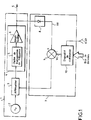
La figure 1, illustre un schéma synoptique simplifié d'un générateur d'ondes radiofréquences comportant un circuit principal 1, représenté à l'intérieur d'une ligne fermée discontinue, et comportant, de l'entrée vers la sortie, un dispositif 2 d'excitation délivrant par exemple un signal de fréquence intermédiaire, Fl, de 1,4 MHz modulé par un signal basse fréquence, dont la sortie est couplée à une première entrée d'un atténuateur commandé 3. La sortie de l'atténuateur 3 est couplée à un dispositif de traitement 4 représenté à l'intérieur d'une ligne fermée continue comportant, par exemple une chaîne de transposition de fréquence 5 couplée à un amplificateur de sortie 6 délivrant sur sa sortie un signal radiofréquence S. Une boucle 7 représentée à l'intérieur d'une ligne fermée discontinue prélève une fraction de la puissance PS du signal S qui est injectée à l'entrée d'un dispositif de détection 8, par exemple à diodes, dont la sortie délivrant une tension Vd est couplée à une première entrée positive d'opérande d'un comparateur 9. Une deuxième entrée d'opérande négative du comparateur 9 reçoit un signal analogique de consigne, par exemple une tension Vc, issue d'un dispositif de commande 10 de l'atténuateur 3 recevant sur une première entrée une tension de référence Vréf et sur une deuxième entrée un bus de données numériques correspondant chacune à une valeur d'atténuation prédéterminée. Le signal issu de la comparaison est injecté sur une deuxième entrée de l'atténuateur 3.FIG. 1 illustrates a simplified block diagram of a radiofrequency generator comprising a main circuit 1, represented inside a discontinuous closed line, and comprising, from the input to the output, a device 2 d excitation delivering for example an intermediate frequency signal, Fl, of 1.4 MHz modulated by a low frequency signal, the output of which is coupled to a first input of a controlled
Un schéma électrique d'un mode de réalisation du dispositif de commande 10 est illustré par la figure 2. Le dispositif de commande 10, représenté à l'intérieur d'une ligne continue, est organisé autour d'un potentiel de référence, par exemple, un potentiel de masse M. II comporte de l'entrée vers la sortie, une première résistance R₁ recevant sur une de ses bornes la tension de référence Vréf, l'autre borne étant couplée à une première entrée d'un CNA 11 recevant sur une deuxième entrée un bus de données numériques. La sortie du CNA 11 est couplée à l'entrée d'un amplificateur 12 à gain fixe, par exemple égal à un, servant d'étage d'adaptation en sortie du dispositif de commande 10. Une résistance R₃ déterminant le gain de l'amplificateur 12 est couplée entre la sortie et l'entrée de l'amplificateur 12. La sortie de l'amplificateur 12 est en outre rebouclée sur l'entrée du CNA 1 1 qui correspond également à une des bornes de la première résistance R₁, par une boucle 13, représentée à l'intérieur d'une ligne discontinue. La boucle 13 comporte une résistance R₂ et une diode D facultative, représentée en traits interrompus, pouvant être couplée entre la résistance R₂ et la première entrée du CNA.An electrical diagram of an embodiment of the
Les trois résistances R₁, R₂ et R₃ du dispositif de commande 10 permettent la détermination du courant de référence Iréf rentrant sur la première entrée du CNA 11 et conditionnent l'allure quasi exponentielle de la tension de consigne Vc en sortie de l'amplificateur 12.The three resistors R₁, R₂ and R₃ of the
Le signal de sortie, ou tension de consigne, Vc délivré par le dispositif de commande 10 est ensuite injecté sur l'entrée d'opérande négative du comparateur 9.The output signal, or setpoint voltage, V c delivered by the
Dans ce mode de réalisation, l'expression de la tension de consigne Vc , déterminée pour couvrir toute la dynamique de la puissance PS du signal de sortie S du générateur, est donnée par l'équation suivante :![]()
où N correspond à la valeur d'atténuation désirée dont la valeur maximale est définie par la capacité du CNA. Cette capacité détermine également la précision du réglage de la puissance PS du signal de sortie S. Chaque information binaire amenée par le bus est convertie, par exemple à partir d'une table de valeurs prédéterminées, en une tension analogique de consigne Vc à la sortie du CNA. Le courant Iréf est la somme de deux courants définis par l'expression suivante :![]()
![]()
where N corresponds to the desired attenuation value, the maximum value of which is defined by the capacity of the DAC. This capacity also determines the precision of the adjustment of the power P S of the output signal S. Each binary item of information brought by the bus is converted, for example from a table of predetermined values, into an analog reference voltage V c to the exit of the CNA. The current I ref is the sum of two currents defined by the following expression: ![]()
En reportant l'expression (2) dans l'expression (1) la tension Vc s'exprime alors de la manière suivante :
avec la condition aux limites suivante R₃<R₂.By transferring expression (2) into expression (1), the voltage V c is then expressed as follows:
with the following boundary condition R₃ <R₂.
Une application numérique est donnée ci-après à titre d 'exemple.A digital application is given below by way of example.
La dynamique de la puissance PS du signal de sortie S est de 30 dB. Le pas d'atténuation est choisi égal à 3 dB avec une précision sur chaque pas d'atténuation meilleure que 0,5 dB. Pour couvrir cette dynamique de 30 dB, un CNA codé sur huit bits est utilisé. Les valeurs d'atténuation N varient donc de :![]()
Les valeurs des résistances R₁, R₂ et R₃ sont les suivantes : R₁ = 100 KΩ, R₂ = 6,2 KΩ et R₃ = 4,64 KΩ. La tension de référence Vréf est choisie égale à Vréf = 6V.The dynamic range of the power P S of the output signal S is 30 dB. The attenuation step is chosen equal to 3 dB with precision on each attenuation step better than 0.5 dB. To cover this 30 dB dynamic range, an eight-bit coded DAC is used. The attenuation values N therefore vary from: ![]()
The values of the resistances R₁, R₂ and R₃ are the following: R₁ = 100 KΩ, R₂ = 6.2 KΩ and R₃ = 4.64 KΩ. The reference voltage V ref is chosen equal to V ref = 6V.
L'expression (3) compte tenu des valeurs ci-dessus permet de relever la caractéristique tension de consigne Vc en fonction de l'atténuation N. Pour cet exemple, la valeur maximale de la tension de consigne pour N proche de 1 est égale à Vc = 1,1V. Cette application numérique est illustrée par les courbes des figures 3a et 3b. Sur la figure 3a l'axe des ordonnées correspond à la tension de consigne Vc gradué de 0V à 1,1V et l'axe des abscisses correspond aux valeurs d'atténuation N. La courbe de la figure 3a est mise en concordance avec celle de la figure 3b qui représente la variation de la tension détectée Vd représentée par l'axe des ordonnées en fonction de la dynamique de la puissance Ps du signal de sortie S représentée par l'axe des abscisses. Deux intervalles de dix pas consécutifs sont choisis respectivement en début et en fin de caractéristique Vc fonction de N, ces intervalles sont reportés sur la caractéristique Vd fonction de la dynamique de PS, et la variation de dynamique obtenue est quasiment identique en début et en fin de dynamique, et de l'ordre de 2 dB dans cet exemple, soit une précision de l'ordre de 0,2 dB par pas. L'échelle des axes des abscisses des deux figures n'étant pas respectée, les axes des abscisses et les courbes sont partiellement interrompus.Expression (3) taking into account the above values makes it possible to raise the characteristic voltage setpoint V c as a function of the attenuation N. For this example, the maximum value of the voltage setpoint for N close to 1 is equal at V c = 1.1V. This digital application is illustrated by the curves of Figures 3a and 3b. In Figure 3a, the ordinate axis corresponds to the setpoint voltage V c graduated from 0V to 1.1V and the abscissa axis corresponds to the attenuation values N. The curve in Figure 3a is brought into line with that of FIG. 3b which represents the variation of the detected voltage V d represented by the ordinate axis as a function of the dynamics of the power P s of the output signal S represented by the abscissa axis. Two intervals of ten consecutive steps are chosen respectively at the start and at the end of characteristic V c as a function of N, these intervals are plotted on the characteristic V d as a function of the dynamics of P S , and the variation in dynamics obtained is almost identical at the start and at the end of the dynamics, and of the order of 2 dB in this example, ie a precision of the order of 0.2 dB per step. The scale of the abscissa axes of the two figures not being respected, the abscissa axes and the curves are partially interrupted.
La diode D n'est pas indispensable au fonctionnement du générateur selon l'invention néanmoins elle aide à la détermination des valeurs des résistances R₁ et R₃ du dispositif de commande 10 dans la zone de fonctionnement ou la diode D est bloquée, c'est-à-dire pour les valeurs de la tension de consigne Vc inférieures à la tension de seuil de détection de la diode.D Tant que la tension de consigne Vc n'a pas atteinte la tension de seuil de la diode D, la boucle 13 du dispositif de commande 10 n'est pas activée. La caractéristique Vc en fonction des valeurs d'atténuation N se réduit alors à une droite dont la pente est fonction de la valeur des résistances R₁ et R₃ pour obtenir une précision en dB suffisante par pas d'atténuation dans le bas de la caractéristique Vc fonction de N. Dans la zone de conduction de la diode D, la boucle 13 est activée et l'allure de la caractéristique devient alors quasi exponentielle, telle qu'illustrée par la figure 3a, avec une pente de départ identique à la pente donnée par le dispositif de commande 10, la boucle 13 étant désactivée. La caractéristique suit alors au plus près la variation de la tension détectée Vd fonction de la dynamique de la puissance PS du signal de sortie S.The diode D is not essential for the operation of the generator according to the invention nevertheless it helps in the determination of the values of the resistances R₁ and R₃ of the
Claims (2)
Applications Claiming Priority (2)
| Application Number | Priority Date | Filing Date | Title |
|---|---|---|---|
| FR9214639 | 1992-12-04 | ||
| FR9214639A FR2699020B1 (en) | 1992-12-04 | 1992-12-04 | Radiofrequency wave generator with variable and regulated output power. |
Publications (1)
| Publication Number | Publication Date |
|---|---|
| EP0600802A1 true EP0600802A1 (en) | 1994-06-08 |
Family
ID=9436242
Family Applications (1)
| Application Number | Title | Priority Date | Filing Date |
|---|---|---|---|
| EP93402933A Ceased EP0600802A1 (en) | 1992-12-04 | 1993-12-03 | RF generator with variable and regulated output power |
Country Status (2)
| Country | Link |
|---|---|
| EP (1) | EP0600802A1 (en) |
| FR (1) | FR2699020B1 (en) |
Citations (3)
| Publication number | Priority date | Publication date | Assignee | Title |
|---|---|---|---|---|
| DE3236148A1 (en) * | 1982-09-29 | 1984-03-29 | Siemens AG, 1000 Berlin und 8000 München | Circuit arrangement for setting the gain of an amplifier |
| DE3433901A1 (en) * | 1984-09-14 | 1986-03-27 | Siemens AG, 1000 Berlin und 8000 München | Circuit for controlling the power of high-frequency transmitters |
| EP0414352A2 (en) * | 1989-06-26 | 1991-02-27 | ORBITEL MOBILE COMMUNICATIONS LIMITED (Reg. no. 2515004) | Radio transmitter with output power control |
-
1992
- 1992-12-04 FR FR9214639A patent/FR2699020B1/en not_active Expired - Fee Related
-
1993
- 1993-12-03 EP EP93402933A patent/EP0600802A1/en not_active Ceased
Patent Citations (3)
| Publication number | Priority date | Publication date | Assignee | Title |
|---|---|---|---|---|
| DE3236148A1 (en) * | 1982-09-29 | 1984-03-29 | Siemens AG, 1000 Berlin und 8000 München | Circuit arrangement for setting the gain of an amplifier |
| DE3433901A1 (en) * | 1984-09-14 | 1986-03-27 | Siemens AG, 1000 Berlin und 8000 München | Circuit for controlling the power of high-frequency transmitters |
| EP0414352A2 (en) * | 1989-06-26 | 1991-02-27 | ORBITEL MOBILE COMMUNICATIONS LIMITED (Reg. no. 2515004) | Radio transmitter with output power control |
Non-Patent Citations (1)
| Title |
|---|
| R. F. WOLFFENBUTTEL: "digitally programmable accurate current sources for logarithmic control of the amplification or attenuation in a gain cell.", IEEE JOURNAL OF SOLID-STATE CIRCUITS, vol. 23, no. 3, June 1988 (1988-06-01), NEW YORK US, pages 767 - 773, XP001093045, DOI: doi:10.1109/4.317 * |
Also Published As
| Publication number | Publication date |
|---|---|
| FR2699020A1 (en) | 1994-06-10 |
| FR2699020B1 (en) | 1995-01-06 |
Similar Documents
| Publication | Publication Date | Title |
|---|---|---|
| EP0583186B1 (en) | Control unit for stabilising the ouput power of laser diodes | |
| FR2662557A1 (en) | LOW VOLTAGE-HIGH VOLTAGE CONVERTER. | |
| FR2708399A1 (en) | Amplifier polarization control system. | |
| EP0567380B1 (en) | Method and device for compensation of phase instabilities of a wave amplified by a microwave tube | |
| EP0278193B1 (en) | Circuit for measuring the dc component of the primary winding current of the output transformer of an inverted rectifier | |
| EP0011534B1 (en) | Method and apparatus for processing analog, in particular pseudoperiodic signals | |
| EP0065901A1 (en) | Potentiometric transducer system | |
| EP0600802A1 (en) | RF generator with variable and regulated output power | |
| EP0809342A1 (en) | Arrangement for controlling the charge of a modular assembly of electrochemical cells connected in series and corresponding module for measuring the cells | |
| FR2712751A1 (en) | Method and device for controlling the gain of a high frequency signal amplifier | |
| EP0010010A1 (en) | Threshold device for distinguishing between black and white on a document and facsimile transmitter comprising such a device | |
| FR2467407A1 (en) | DEVICE FOR MEASURING VALUES CREATED FROM A NON-PERIODIC PHENOMENON WITH LOW RECURRENCE | |
| EP0308293B1 (en) | Controlled output power device for a class-c amplifier | |
| EP0530072B1 (en) | Method and device for control and regulation | |
| EP0689061A1 (en) | Device for measuring the state of charge of an electrochemical generator | |
| EP0678751B1 (en) | Detector for variations of a supply voltage | |
| EP0050583B1 (en) | Alternating voltage to direct current converter and oscillator circuit comprising said converter | |
| EP0159263A1 (en) | Method and apparatus for controlling the liquid level in a tank | |
| EP0549464A1 (en) | Method and apparatus for measuring the state of charge of an electrochemical generator | |
| EP0047683A1 (en) | Error detecting device for a ternary coded signal | |
| EP0851563B1 (en) | Switch mode power supply device with controlled electromagnetic pertubation | |
| EP1394939B1 (en) | Closed-loop control of an analog system producing an output signal from a control signal | |
| FR2490404A1 (en) | Instrumentation on avalanche photo diode gain stabilisation circuit - uses comparison between normal unity gain photocurrent and avalanche current to regulate reverse bias voltage | |
| EP0063516B1 (en) | Method of measuring gain variations of a laser amplifier and device for carrying out the method | |
| EP0838901B1 (en) | Analogue to digital conversion device with regulated input dynamic range |
Legal Events
| Date | Code | Title | Description |
|---|---|---|---|
| PUAI | Public reference made under article 153(3) epc to a published international application that has entered the european phase |
Free format text: ORIGINAL CODE: 0009012 |
|
| AK | Designated contracting states |
Kind code of ref document: A1 Designated state(s): DE GB IT |
|
| 17P | Request for examination filed |
Effective date: 19941126 |
|
| GRAG | Despatch of communication of intention to grant |
Free format text: ORIGINAL CODE: EPIDOS AGRA |
|
| 17Q | First examination report despatched |
Effective date: 19970117 |
|
| STAA | Information on the status of an ep patent application or granted ep patent |
Free format text: STATUS: THE APPLICATION HAS BEEN REFUSED |
|
| 18R | Application refused |
Effective date: 19970821 |