EP0678751B1 - Detector for variations of a supply voltage - Google Patents
Detector for variations of a supply voltage Download PDFInfo
- Publication number
- EP0678751B1 EP0678751B1 EP19950400862 EP95400862A EP0678751B1 EP 0678751 B1 EP0678751 B1 EP 0678751B1 EP 19950400862 EP19950400862 EP 19950400862 EP 95400862 A EP95400862 A EP 95400862A EP 0678751 B1 EP0678751 B1 EP 0678751B1
- Authority
- EP
- European Patent Office
- Prior art keywords
- voltage
- supply voltage
- value
- mos transistor
- detector circuit
- Prior art date
- Legal status (The legal status is an assumption and is not a legal conclusion. Google has not performed a legal analysis and makes no representation as to the accuracy of the status listed.)
- Expired - Lifetime
Links
- 238000001514 detection method Methods 0.000 claims description 20
- 230000001052 transient effect Effects 0.000 claims description 11
- 238000005070 sampling Methods 0.000 claims description 5
- 238000005265 energy consumption Methods 0.000 claims description 2
- 238000004519 manufacturing process Methods 0.000 claims description 2
- 230000000737 periodic effect Effects 0.000 claims description 2
- 230000001747 exhibiting effect Effects 0.000 claims 1
- 238000009434 installation Methods 0.000 claims 1
- 238000012360 testing method Methods 0.000 description 20
- 230000000903 blocking effect Effects 0.000 description 5
- 238000010586 diagram Methods 0.000 description 4
- 238000005516 engineering process Methods 0.000 description 3
- 238000004377 microelectronic Methods 0.000 description 3
- 238000012544 monitoring process Methods 0.000 description 3
- 238000000034 method Methods 0.000 description 2
- 230000000747 cardiac effect Effects 0.000 description 1
- 235000021183 entrée Nutrition 0.000 description 1
- 230000010354 integration Effects 0.000 description 1
- 238000012806 monitoring device Methods 0.000 description 1
- 238000011160 research Methods 0.000 description 1
- 238000012546 transfer Methods 0.000 description 1
Images

Classifications
-
- G—PHYSICS
- G01—MEASURING; TESTING
- G01R—MEASURING ELECTRIC VARIABLES; MEASURING MAGNETIC VARIABLES
- G01R19/00—Arrangements for measuring currents or voltages or for indicating presence or sign thereof
- G01R19/165—Indicating that current or voltage is either above or below a predetermined value or within or outside a predetermined range of values
- G01R19/16533—Indicating that current or voltage is either above or below a predetermined value or within or outside a predetermined range of values characterised by the application
- G01R19/16538—Indicating that current or voltage is either above or below a predetermined value or within or outside a predetermined range of values characterised by the application in AC or DC supplies
Definitions
- the present invention relates to a device for voltage variation detection power supply.
- a person skilled in the art can compare the value of a voltage to be monitored, such as the value of the voltage of a storage battery, to a value of threshold, so as to generate a signal when crossing of this threshold value by the voltage to be monitored.
- a comparator allows at most to detect the only crossing of the value threshold, without giving information such as the nature transient or not of this crossing, except to provide for filter circuits for transient disturbances of this voltage to monitor.
- CMOS Power-on detection circuit Research Disclosure No. 335, March 1992, Emsworth, GB, pages 224 to 225 describes a detector of this kind.
- the triggering of these comparators implies a trigger either by values higher, or by lower values, the implementation monitoring devices usable both at initialization or starting these devices until the end of lifespan of their supply storage battery actually involving the doubling of these devices by putting in parallel with this type of comparators, one triggering on overshoot by higher values, the other by values lower.
- the object of the present invention is to remedy the abovementioned drawbacks of the devices of the prior art by the implementation of a device for detecting the notably non-transient variation of a supply voltage making it possible to deliver a detected signal of constant value, as long as the supply voltage is greater than one determined threshold value, and a detected signal whose value is equal to that of the supply voltage, as long that the latter is less than said threshold value.
- Another object of the present invention is the implementation using a device for detecting variation, especially not transient of an electrical supply voltage allowing perform level control and monitoring the supply voltage of electronic devices, micro-electronics or IT, at the cost of a very low consumption of electrical energy from this source Power.
- the variation detection device of a supply voltage with respect to a reference voltage is remarkable in that it includes a detector circuit asymmetric threshold of a voltage variation comprising a reference input connected to the reference voltage, and a detection input supplied by the supply voltage via a first potentiometric divider.
- the threshold detector circuit makes it possible to deliver a variable voltage from copy reference voltage variations, with the same slope, of the supply voltage.
- a level comparator circuit is provided, this circuit with a negative comparison input and a positive comparison input. Comparison entry negative is connected to the threshold detector circuit and receives variable voltage and comparison input positive is connected to the supply voltage via a second potentiometric, adjustable divider, controlled by the output of the level comparator circuit.
- the level comparator circuit generates on its output a signal whose value is equal to either the value of the supply voltage, when the latter is lower or equal to a threshold value, or to the value of the reference voltage when the supply voltage is greater than this threshold value.
- the detection device object of the invention finds application in the electronics or microelectronics industry for the implementation of control circuits or equipment supply voltage monitoring computer or micro-electronic, portable, implanted or automotive electronics.
- the device which is the subject of the present invention comprises a circuit 1 detector with asymmetric threshold of a voltage variation, this circuit making it possible, from the reference voltage, denoted V REF , to deliver a variable voltage, which is a copy of the variations, with the same slope, of the supply voltage noted V CC .
- the transfer function of the detector circuit 1 is shown in Figures 2a and 2b, which will be explained later in the description.
- the threshold detector circuit 1 comprises a reference input connected to the reference voltage V REF , and a detection input.
- the detection input is supplied by the supply voltage V DC via a first potentiometric divider.
- the first potentiometric divider as shown in FIG. 2a, delivers from the supply voltage V CC when this is subjected to variations, a signal represented, corresponding to the test point.
- this variation being represented between the reference voltage V REF and the supply voltage V CC with a slope k 1 when, for example, powering up the assembly of the detection device shown in FIG. 1
- the first potentiometric divider device delivering to the input of the detector circuit 1 a corresponding voltage with a slope of value k ′ 1 , as shown for the test point B in FIG. 1 in phantom in FIG. 2a.
- the threshold detector circuit 1 makes it possible to deliver, as shown in FIG. 2a, the signal as represented at the test point C in FIG. 1, this signal corresponding to the variable voltage, with the same slope k 1 as that of the variation of the supply voltage with a delay due to the asymmetry of the threshold of the detector, this delay being noted ⁇ t in FIG. 2a.
- the detection device object of the present invention includes a level comparator circuit 2, comprising a negative comparison input and a positive comparison input. Comparison entry negative is connected at the output of the detector circuit to threshold 1 and receives the variable voltage, as shown in Figure 2, while the positive comparison input of comparator circuit 2 is connected to the supply voltage via a second potentiometric divider adjustable, controlled by the output of the comparator circuit level 2.
- the operation of the detection device shown in FIG. 1 is as follows: for a variation of the supply voltage V CC from a substantially stable starting voltage value, when the power is turned on at an instant t 0 of the assembly for example starting from a zero value corresponding to the reference voltage V REF , the voltage delivered to the test point D of FIG. 1 corresponding to the positive input of the level 2 comparator circuit, evolves with a slope k 2 , as shown in FIG. 2a, less than the slope k 1 of the variable voltage delivered by the threshold detector circuit 1.
- the output signal Vs delivered by the level 2 comparator circuit is none other than the supply voltage V DC , as long as the variable voltage delivered by the threshold detector circuit 1 is lower than the signal delivered by the second potentiometric divider at the positive comparison input of the level comparator circuit 2.
- the level 2 comparator circuit causes switching and the output voltage Vs previously equal to the aforementioned variable voltage and delivers, on switching, a constant voltage equal to the reference voltage V REF .
- FIG. 2a also shows a variation in the supply voltage from the maximum value V CCmax with an opposite slope -k 1 .
- the value of the voltage at the test point D is for example equal to V DC , fixed by the switched value of the second potentiometer.
- the value of the voltage at the test point D is for example equal to V D , fixed by the unswitched value of the second potentiometer.
- variable voltage at point C evolves with the same slope -k 1 from the initial value V C.
- the voltage at point D also changes from the initial value V D or V DC with or without a return to the initial value, with a slope -k 2 respectively -k 3 depending on the unswitched value or of the second potentiometric divider.
- voltage values of the intersection point C V C and V D or V DC at point D spoke to a threshold value V respectively seuil2c threshold2 V of the supply voltage.
- the voltages V threshold1 and V threshold2 are different, since they depend on the initial values V D , V DC .
- the first potentiometric divider can comprise, connected in cascade between the supply voltage V CC and the reference voltage V REF , a circuit 3 of current type constant making it possible to attenuate the transient variations of the supply voltage V CC at the input of the level comparator circuit 1.
- this circuit 3 can be constituted by a current generator, which, due to the current imposed by the latter, substantially imposes on the test point A of FIG. 1 a DC voltage substantially equal to the supply voltage V CC at this point.
- the second potentiometric divider it is indicated that it can be formed by, successively connected between the supply voltage V CC and the reference voltage V REF , a programmable adjustable impedance Z3, a resistor Z4 and a resistor Z5, the impedances or resistors Z3 to Z5 being connected between the supply voltage and the reference voltage V REF , the common point between the resistance Z4 and the resistance Z5 being connected to the positive comparison input of the level comparator circuit 2.
- the impedance Z3 When switching via the output voltage Vs, it is indicated that the impedance Z3 is brought to a value greater than the abovementioned initial value, this value of Z3 being chosen so that, after switching by the intermediate of the output voltage Vs, the voltage at the test point D delivered by the second potentiometric divider is either less than the voltage delivered on the negative comparison input of the level 2 comparator circuit, or at the intersection value of the curves of slope k 1 and k 2 in Figure 2.
- Figure 2b shows the corresponding timing diagram for the output voltage Vs delivered by the comparator output level 2.
- the threshold detector circuit 1 can advantageously comprise a first, a second, a third and a fourth MOS transistor, referenced 11, 12, 13, 14 respectively, connected in series between the voltage d V DC supply and the reference voltage V REF .
- the first and second MOS transistors 11 and 12 are of the same first type of conduction, type P in the case of the representation of FIG. 3b, and the third and fourth MOS transistors 13 and 14 are of a second type of conduction , opposite to the first type, and therefore of type N in the case of the representation of FIG. 3b.
- the first divider bridge as shown by example in Figure 3a, is then connected in parallel to from the common point between the impedances Z1 and Z2 at the grid of the first, second, third and fourth transistors MOS 11, 12, 13 and 14.
- the source and drain electrodes of the fifth MOS transistor 15 are connected between the common point of the first and of the second MOS transistor 11, 12 and the reference voltage V REF .
- the fifth MOS transistor 15 has a resistance much higher than that of the first MOS transistor 11 in a ratio 1000 about.
- the drain and source electrodes of the sixth MOS transistor 16 are connected between the supply voltage V CC and the common point between the third and the fourth MOS transistor 13, 14 previously mentioned.
- test E which correspond respectively to the points test B of Figure 1, in common with the second and the third MOS transistor 12, 13, i.e. at the gate of the fifth MOS transistor 15, and in common between the first and the second MOS transistor 11, 12 as well than at the test points C in FIG. 1, that is to say in output of the threshold detector circuit 1 of FIG. 1.
- test points E and F are first of all at zero. During the rise of the supply voltage to the value V CCmax with the slope k 1 , the voltage at the test point G, that is to say at the output of the threshold detector circuit, remains at the value of the reference voltage V REF . It is the same for the test point F due to the absence of conduction of the first, second, third and fourth MOS transistors 11 to 14.
- variable voltage delivered by the threshold detector circuit 1 also follows the slope of this variable supply voltage due to the value of the above impedances.
- the circuit for attenuation of the transient variations of the supply voltage V CC , the circuit 3, and more specifically the current generator 30, can be produced by CMOS technology, which of course allows, from an embodiment as shown in FIG. 3b for the threshold detector circuit 1 and for the level 2 comparator circuit, to envisage the realization of the detection device object of the present invention in the form of an integrated circuit.
- the impedances Z1 to Z5 can also be produced by means of MOS type transistors, which can allow the production of resistances of good precision.
- adjustable impedance Z3 With regard more particularly to the adjustable impedance Z3, it is indicated that this can be achieved in the form of programmable impedances by means of MOS circuits so as to also allow the integration of the assembly.
- the final values V D, V DC and V threshold 1 threshold, V threshold2, V seuil2c can thus be adjusted.
- the detection device object of the present invention can advantageously include a control circuit 4 allowing to issue a commissioning or blocking signal, this signal being noted SCFB in FIG. 1 above.
- This start-up or blocking signal allows by example of ensuring the commissioning or blocking of the current generator 3 and level 2 comparator, this which controls the operation or stopping of the entire detection device by blocking or setting operation of threshold detector circuits 1, comparator level 2 and current generator 3.
- the circuit of command 4 can simply issue a blocking signal or authorizing the supply of the filter circuit 3 and the level 2 comparator circuit, for example.
- control circuit 4 can deliver a signal periodic, which allows for a sampled order the operation of the device, in order to obtain a reduction of the overall energy consumption of the device shown in figure 1.
- the period and the sampling times are programmable and modular depending on the application considered. So when the detection device object of the present invention is used to control and monitor supply voltage of a laptop for example, the period sample can be set for example to a value ten minutes, the sampling time itself being for example a few hundred ms.
- the sampling period may be extended to a much longer period, one to many hours for example.
- Figures 4a and 4b show the appearance of voltage variations at test point C and D in the figure 1 respectively of a variable supply voltage and the corresponding output voltage Vs.
- This device has great flexibility of use insofar as the operation of the latter can be controlled either manually or automatically according to a sampled mode.
Landscapes
- Engineering & Computer Science (AREA)
- Power Engineering (AREA)
- Physics & Mathematics (AREA)
- General Physics & Mathematics (AREA)
- Measurement Of Current Or Voltage (AREA)
Description
La présente invention concerne un dispositif de détection de la variation d'une tension d'alimentation électrique.The present invention relates to a device for voltage variation detection power supply.
Dans les systèmes informatiques ou électroniques actuels, la notion d'autonomie de ces systèmes est primordiale. Indépendamment de l'autonomie effective de ces derniers, en particulier lorsqu'ils sont mis en oeuvre sous forme de matériels embarqués portables voire implantés, il est de la plus haute importance de pouvoir contrôler et surveiller l'évolution de la tension d'alimentation électrique de ces appareils, lorsque notamment ceux-ci sont alimentés à partir de batteries d'accumulateurs rechargeables par exemple.In computer or electronic systems At present, the notion of autonomy of these systems is essential. Regardless of the effective autonomy of these last, especially when implemented under form of on-board portable or even implanted equipment, it is of the utmost importance to be able to control and monitor the evolution of the power supply voltage of these devices, especially when these are powered from rechargeable batteries by example.
De manière classique, l'homme de l'art sait comparer la valeur d'une tension à surveiller, telle que la valeur de la tension d'une batterie d'accumulateurs, à une valeur de seuil, de manière à engendrer un signal lors du franchissement de cette valeur de seuil par la tension à surveiller. Ce mode opératoire à partir d'un comparateur permet cependant au plus de détecter le seul franchissement de la valeur de seuil, sans donner d'information telle que la nature transitoire ou non de ce franchissement, sauf à prévoir des circuits de filtrage des perturbations transitoires de cette tension à surveiller.Conventionally, a person skilled in the art can compare the value of a voltage to be monitored, such as the value of the voltage of a storage battery, to a value of threshold, so as to generate a signal when crossing of this threshold value by the voltage to be monitored. However, this procedure using a comparator allows at most to detect the only crossing of the value threshold, without giving information such as the nature transient or not of this crossing, except to provide for filter circuits for transient disturbances of this voltage to monitor.
Le document "CMOS Power-on detection circuit", Research Disclosure No. 335, Mars 1992, Emsworth, GB, pages 224 à 225 décrit un détecteur de ce genre.The document "CMOS Power-on detection circuit", Research Disclosure No. 335, March 1992, Emsworth, GB, pages 224 to 225 describes a detector of this kind.
En outre, en général le déclenchement de ces comparateurs implique un déclenchement soit par valeurs supérieures, soit par valeurs inférieures, la mise en oeuvre de dispositifs de surveillance utilisables tant à l'initialisation ou mise en route de ces appareils qu'en fin de durée de vie de leur batterie d'accumulateurs d'alimentation impliquant en fait le doublement de ces dispositifs par mise en parallèle de ce type de comparateurs, l'un déclenchant sur dépassement par valeurs supérieures, l'autre par valeurs inférieures.In addition, in general the triggering of these comparators implies a trigger either by values higher, or by lower values, the implementation monitoring devices usable both at initialization or starting these devices until the end of lifespan of their supply storage battery actually involving the doubling of these devices by putting in parallel with this type of comparators, one triggering on overshoot by higher values, the other by values lower.
La présente invention a pour objet de remédier aux inconvénients précités des dispositifs de l'art antérieur par la mise en oeuvre d'un dispositif de détection de la variation notamment non transitoire d'une tension d'alimentation permettant de délivrer un signal détecté de valeur constante, tant que la tension d'alimentation est supérieure à une valeur de seuil déterminée, et un signal détecté dont la valeur est égale à celle de la tension d'alimentation, tant que cette dernière est inférieure à ladite valeur de seuil.The object of the present invention is to remedy the abovementioned drawbacks of the devices of the prior art by the implementation of a device for detecting the notably non-transient variation of a supply voltage making it possible to deliver a detected signal of constant value, as long as the supply voltage is greater than one determined threshold value, and a detected signal whose value is equal to that of the supply voltage, as long that the latter is less than said threshold value.
Un autre objet de la présente invention est la mise en oeuvre d'un dispositif de détection de la variation notamment non transitoire d'une tension d'alimentation électrique permettant d'effectuer un contrôle et une surveillance du niveau de la tension d'alimentation d'appareils électroniques, micro-électroniques ou informatiques, au prix d'une très faible consommation de l'énergie électrique de cette source d'alimentation.Another object of the present invention is the implementation using a device for detecting variation, especially not transient of an electrical supply voltage allowing perform level control and monitoring the supply voltage of electronic devices, micro-electronics or IT, at the cost of a very low consumption of electrical energy from this source Power.
Le dispositif de détection de la variation d'une tension d'alimentation par rapport à une tension de référence, objet de la présente invention, est remarquable en ce qu'il comprend un circuit détecteur à seuil asymétrique d'une variation de tension comprenant une entrée de référence connectée à la tension de référence, et une entrée de détection alimentée par la tension d'alimentation par l'intermédiaire d'un premier diviseur potentiométrique. Le circuit détecteur à seuil permet de délivrer une tension variable à partir de la tension de référence copie des variations, avec la même pente, de la tension d'alimentation. Un circuit comparateur de niveau est prévu, ce circuit comportant une entrée de comparaison négative et une entrée de comparaison positive. L'entrée de comparaison négative est connectée au circuit détecteur à seuil et reçoit la tension variable et l'entrée de comparaison positive est reliée à la tension d'alimentation par l'intermédiaire d'un deuxième diviseur potentiométrique, ajustable, commandé par la sortie du circuit comparateur de niveau. Le circuit comparateur de niveau engendre sur sa sortie un signal dont la valeur est égale soit à la valeur de la tension d'alimentation, lorsque cette dernière est inférieure ou égale à une valeur de seuil, soit à la valeur de la tension de référence lorsque la tension d'alimentation est supérieure à cette valeur de seuil.The variation detection device of a supply voltage with respect to a reference voltage, object of the present invention, is remarkable in that it includes a detector circuit asymmetric threshold of a voltage variation comprising a reference input connected to the reference voltage, and a detection input supplied by the supply voltage via a first potentiometric divider. The threshold detector circuit makes it possible to deliver a variable voltage from copy reference voltage variations, with the same slope, of the supply voltage. A level comparator circuit is provided, this circuit with a negative comparison input and a positive comparison input. Comparison entry negative is connected to the threshold detector circuit and receives variable voltage and comparison input positive is connected to the supply voltage via a second potentiometric, adjustable divider, controlled by the output of the level comparator circuit. The level comparator circuit generates on its output a signal whose value is equal to either the value of the supply voltage, when the latter is lower or equal to a threshold value, or to the value of the reference voltage when the supply voltage is greater than this threshold value.
Le dispositif de détection objet de l'invention trouve application dans l'industrie électronique ou microélectronique pour la mise en oeuvre de circuits de contrôle ou de surveillance de la tension d'alimentation de matériels informatiques ou micro-électroniques, portables, implantés ou d'électronique automobile.The detection device object of the invention finds application in the electronics or microelectronics industry for the implementation of control circuits or equipment supply voltage monitoring computer or micro-electronic, portable, implanted or automotive electronics.
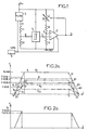
Il sera mieux compris à la lecture de la description et à l'observation des dessins ci-après dans lesquels :
- la figure 1 représente, sous forme de blocs fonctionnels, un schéma synoptique du dispositif objet de la présente invention,
- les figures 2a, 2b montrent un chronogramme des variations de tension lors de l'établissement et de la coupure, par exemple, de la tension d'alimentation,
- la figure 3a représente un détail de réalisation du premier pont diviseur permettant de supprimer les variations transitoires de la tension d'alimentation transmises à l'entrée du détecteur à seuil,
- la figure 3b représente un mode de réalisation particulier, non limitatif, du détecteur à seuil en technologie CMOS,
- les figures 4a et 4b représentent différents chronogrammes de signaux aux points de test de la figure 1.
- FIG. 1 represents, in the form of functional blocks, a block diagram of the device which is the subject of the present invention,
- FIGS. 2a, 2b show a timing diagram of the voltage variations during the setting up and switching off, for example, of the supply voltage,
- FIG. 3a shows a detail of the first divider bridge making it possible to eliminate the transient variations in the supply voltage transmitted to the input of the threshold detector,
- FIG. 3b represents a particular, non-limiting embodiment of the threshold detector in CMOS technology,
- FIGS. 4a and 4b represent different timing diagrams of signals at the test points of FIG. 1.
Le dispositif de détection de la variation notamment non transitoire d'une tension d'alimentation électrique, objet de la présente invention, sera maintenant décrit en liaison avec les figures 1 et suivantes.The variation detection device in particular not transient of a power supply voltage, object of the present invention will now be described in connection with Figures 1 and following.
Selon la figure 1 précitée, on indique que le
dispositif objet de la présente invention comprend un
circuit 1 détecteur à seuil asymétrique d'une variation de
tension, ce circuit permettant, à partir de la tension de
référence, notée VREF, de délivrer une tension variable,
laquelle est une copie des variations, avec la même pente,
de la tension d'alimentation notée VCC.According to FIG. 1 above, it is indicated that the device which is the subject of the present invention comprises a
La fonction de transfert du circuit détecteur 1 est
représentée en figures 2a et 2b, lesquelles seront explicitées
ultérieurement dans la description. Le circuit détecteur
à seuil 1 comprend une entrée de référence connectée à
la tension de référence VREF, et une entrée de détection.
L'entrée de détection est alimentée par la tension d'alimentation
VCC par l'intermédiaire d'un premier diviseur potentiométrique.
On indique d'une manière générale que le
premier diviseur potentiométrique, ainsi que représenté en
figure 2a, délivre à partir de la tension d'alimentation VCC
lorsque celle-ci est soumise à des variations, un signal
représenté, correspondant au point de test A de la figure 1,
cette variation étant représentée entre la tension de
référence VREF et la tension d'alimentation VCC avec une pente
k1 lors par exemple de la mise sous tension de l'ensemble du
dispositif de détection représenté en figure 1, le premier
dispositif diviseur potentiométrique délivrant à l'entrée du
circuit détecteur 1 une tension correspondante avec une
pente de valeur k'1, ainsi que représenté pour le point de
test B de la figure 1 en trait mixte sur la figure 2a.The transfer function of the
Le circuit détecteur à seuil 1 permet de délivrer,
ainsi que représenté en figure 2a, le signal tel que représenté
au point de test C de la figure 1, ce signal correspondant
à la tension variable, avec la même pente k1 que
celle de la variation de la tension d'alimentation avec un
retard dû à l'asymétrie du seuil du détecteur, ce retard
étant noté Δt sur la figure 2a.The
En outre, le dispositif de détection objet de la
présente invention comprend un circuit comparateur de niveau
2, comportant une entrée de comparaison négative et une
entrée de comparaison positive. L'entrée de comparaison
négative est connectée en sortie du circuit détecteur à
seuil 1 et reçoit la tension variable, tel que représentée
en figure 2, alors que l'entrée de comparaison positive du
circuit comparateur 2 est reliée à la tension d'alimentation
par l'intermédiaire d'un deuxième diviseur potentiométrique
ajustable, commandé par la sortie du circuit comparateur de
niveau 2.In addition, the detection device object of the
present invention includes a
Le fonctionnement du dispositif de détection
représenté en figure 1 est le suivant : pour une variation
de la tension d'alimentation VCC à partir d'une valeur de
tension de départ sensiblement stable, lors de la mise sous
tension à un instant t0 de l'ensemble par exemple à partir
d'une valeur zéro correspondant à la tension de référence
VREF, la tension délivrée au point de test D de la figure 1
correspondant à l'entrée positive du circuit comparateur de
niveau 2, évolue avec une pente k2, ainsi que représenté en
figure 2a, inférieure à la pente k1 de la tension variable
délivrée par le circuit détecteur à seuil 1. En raison du
retard Δt de la tension variable précitée, mais compte tenu
de la pente k1 supérieure à la pente k2 de la tension
variable par rapport à la pente du signal délivré par le
deuxième diviseur potentiométrique, le signal de sortie Vs
délivré par le circuit comparateur de niveau 2 n'est autre
que la tension d'alimentation VCC, tant que la tension
variable délivrée par le circuit détecteur à seuil 1 est
inférieure au signal délivré par le deuxième diviseur
potentiométrique à l'entrée de comparaison positive du
circuit comparateur de niveau 2. Sur dépassement de cette
dernière, ainsi que représenté en figure 2, le circuit
comparateur de niveau 2 provoque une commutation et la
tension de sortie Vs précédemment égale à la tension
variable précitée et délivre, sur commutation, une tension
constante égale à la tension de référence VREF. La commutation
se produit pour une valeur de la tension d'alimentation
égale à Vseuil1. Cette variation de la tension de sortie Vs
provoque alors une commutation de la valeur du deuxième
diviseur potentiométrique précédemment cité, par augmentation
de l'impédance totale du deuxième diviseur potentiométrique
précité, ce qui permet d'abaisser la valeur de la
tension d'entrée appliquée à l'entrée de comparaison
positive du circuit comparateur de niveau 2 à une valeur
basse, le circuit comparateur de niveau 2 délivrant alors en
sortie la tension de sortie Vs dont la valeur est égale à la
tension de référence VREF tant que la tension d'alimentation
VCC reste supérieure à la nouvelle valeur de seuil, définie
par la commutation de la valeur du deuxième diviseur
potentiométrique.The operation of the detection device shown in FIG. 1 is as follows: for a variation of the supply voltage V CC from a substantially stable starting voltage value, when the power is turned on at an instant t 0 of the assembly for example starting from a zero value corresponding to the reference voltage V REF , the voltage delivered to the test point D of FIG. 1 corresponding to the positive input of the
D'une manière générale, on indique que lors d'une variation de la tension d'alimentation à partir d'une valeur d'alimentation maximale VCCmax par exemple, ainsi que représenté en figure 2a, le processus est sensiblement symétrique, le deuxième diviseur potentiométrique ayant été ramené à sa valeur initiale.In general, it is indicated that during a variation of the supply voltage from a maximum supply value V CCmax for example, as shown in FIG. 2a, the process is substantially symmetrical, the second potentiometric divider having been brought back to its initial value.
Sur la figure 2a, on a représenté également une variation de la tension d'alimentation à partir de la valeur maximale VCCmax avec une pente opposée -k1. En l'absence de retour à la valeur initiale du deuxième diviseur potentiométrique, la valeur de la tension au point de test D est par exemple égale à VDC, fixée par la valeur commutée du deuxième potentiomètre. En présence d'un retour à la valeur initiale du deuxième diviseur potentiométrique, la valeur de la tension au point de test D est par exemple égale à VD, fixée par la valeur non commutée du deuxième potentiomètre. Sur variation de la tension d'alimentation VCC à partir de la valeur maximale VCCmax à un instant t1 quelconque, la variation étant une diminution avec une pente -k1 pour fixer les idées, la tension variable au point C évolue avec la même pente -k1 à partir de la valeur initiale VC. La tension au point D évolue en outre à partir de la valeur initiale VD ou VDC en présence ou non d'un retour à la valeur initiale, avec une pente -k2 respectivement -k3 en fonction de la valeur non commutée ou commutée du deuxième diviseur potentiométrique. Ainsi, l'intersection des valeurs de tension VC au point C et VD ou VDC au point D Intervient pour une valeur de seuil Vseuil2 respectivement Vseuil2c de la tension d'alimentation. Dans le cas général, les tensions Vseuil1 et Vseuil2 sont différentes, car dépendant des valeurs initiales VD, VDC.FIG. 2a also shows a variation in the supply voltage from the maximum value V CCmax with an opposite slope -k 1 . In the absence of return to the initial value of the second potentiometric divider, the value of the voltage at the test point D is for example equal to V DC , fixed by the switched value of the second potentiometer. In the presence of a return to the initial value of the second potentiometric divider, the value of the voltage at the test point D is for example equal to V D , fixed by the unswitched value of the second potentiometer. On variation of the supply voltage V CC from the maximum value V CCmax at any time t 1 , the variation being a decrease with a slope -k 1 to fix ideas, the variable voltage at point C evolves with the same slope -k 1 from the initial value V C. The voltage at point D also changes from the initial value V D or V DC with or without a return to the initial value, with a slope -k 2 respectively -k 3 depending on the unswitched value or of the second potentiometric divider. Thus, voltage values of the intersection point C V C and V D or V DC at point D spoke to a threshold value V respectively seuil2c threshold2 V of the supply voltage. In the general case, the voltages V threshold1 and V threshold2 are different, since they depend on the initial values V D , V DC .
Ainsi qu'on l'a en outre représenté en figure 3a, on
indique que le premier diviseur potentiométrique peut
comprendre, connecté en cascade entre la tension d'alimentation
VCC et la tension de référence VREF, un circuit 3 de type
à courant constant permettant d'atténuer les variations
transitoires de la tension d'alimentation VCC à l'entrée du
circuit comparateur de niveau 1. On indique que ce circuit
3 peut être constitué par un générateur de courant, lequel,
en raison du courant imposé par ce dernier, impose sensiblement
au point de test A de la figure 1 une tension continue
sensiblement égale à la tension d'alimentation VCC en ce
point.As has also been represented in FIG. 3a, it is indicated that the first potentiometric divider can comprise, connected in cascade between the supply voltage V CC and the reference voltage V REF , a
Au générateur de courant 30 est connecté un réseau
de résistances Z1, Z2, le point commun de ces résistances
étant relié à l'entrée du circuit détecteur de niveau 1.To the
En ce qui concerne le deuxième diviseur potentiométrique,
on indique que celui-ci peut être formé par,
successivement connectées entre la tension d'alimentation VCC
et la tension de référence VREF, une impédance ajustable
programmable Z3, une résistance Z4 et une résistance Z5, les
impédances ou résistances Z3 à Z5 étant connectées entre la
tension d'alimentation et la tension de référence VREF, le
point commun entre la résistance Z4 et la résistance Z5
étant relié à l'entrée de comparaison positive du circuit
comparateur de niveau 2.With regard to the second potentiometric divider, it is indicated that it can be formed by, successively connected between the supply voltage V CC and the reference voltage V REF , a programmable adjustable impedance Z3, a resistor Z4 and a resistor Z5, the impedances or resistors Z3 to Z5 being connected between the supply voltage and the reference voltage V REF , the common point between the resistance Z4 and the resistance Z5 being connected to the positive comparison input of the
En ce qui concerne la valeur des résistances Z3, Z4, Z5 du deuxième diviseur potentiométrique, on indique que ces valeurs sont choisies de façon à constituer, pour la tension appliquée au point de test D de la figure 1 une valeur de seuil, notée Vseuil, correspondant à l'initialisation à une valeur arbitraire fraction de la tension d'alimentation maximale VCCmax précédemment indiquée dans la description. On indique que pour une tension d'alimentation VCCmax égale à 5 volts, la valeur de seuil ainsi constituée initialement peut être prise égale à Vseuil = 2 volts.As regards the value of the resistors Z3, Z4, Z5 of the second potentiometric divider, it is indicated that these values are chosen so as to constitute, for the voltage applied to the test point D of FIG. 1, a threshold value, denoted V threshold , corresponding to initialization at an arbitrary value fraction of the maximum supply voltage V CCmax previously indicated in the description. It is indicated that for a supply voltage V CCmax equal to 5 volts, the threshold value thus formed initially can be taken equal to V threshold = 2 volts.
Lors de la commutation par l'intermédiaire de la
tension de sortie Vs, on indique que l'impédance Z3 est
amenée à une valeur plus importante que la valeur initiale
précitée, cette valeur de Z3 étant choisie de façon que,
après commutation par l'intermédiaire de la tension de
sortie Vs, la tension au point de test D délivrée par le
deuxième diviseur potentiométrique soit inférieure à la
tension délivrée sur l'entrée de comparaison négative du
circuit comparateur de niveau 2, soit à la valeur d'intersection
des courbes de pente k1 et k2 sur la figure 2.When switching via the output voltage Vs, it is indicated that the impedance Z3 is brought to a value greater than the abovementioned initial value, this value of Z3 being chosen so that, after switching by the intermediate of the output voltage Vs, the voltage at the test point D delivered by the second potentiometric divider is either less than the voltage delivered on the negative comparison input of the
La figure 2b montre le chronogramme correspondant de
la tension de sortie Vs délivrée par la sortie du comparateur
de niveau 2.Figure 2b shows the corresponding timing diagram for
the output voltage Vs delivered by the
Une description plus détaillée du circuit détecteur
à seuil 1 sera maintenant donnée en liaison avec la figure
3b.A more detailed description of the detector circuit
at
Dans le mode de réalisation précité, on indique que
le circuit détecteur à seuil 1 peut comprendre avantageusement
un premier, un deuxième, un troisième et un quatrième
transistor MOS, référencés 11, 12, 13, 14 respectivement,
connectés en série entre la tension d'alimentation VCC et la
tension de référence VREF. Les premier et deuxième transistors
MOS 11 et 12 sont d'un même premier type de conduction,
type P dans le cas de la représentation de la figure 3b, et
les troisième et quatrième transistors MOS 13 et 14 sont
d'un deuxième type de conduction, opposé au premier type, et
donc de type N dans le cas de la représentation de la
figure 3b.In the aforementioned embodiment, it is indicated that the
Le premier pont diviseur, tel que représenté par
exemple en figure 3a, est alors connecté en parallèle à
partir du point commun entre les impédances Z1 et Z2 à la
grille du premier, deuxième, troisième et quatrième transistors
MOS 11, 12, 13 et 14.The first divider bridge, as shown by
example in Figure 3a, is then connected in parallel to
from the common point between the impedances Z1 and Z2 at the
grid of the first, second, third and
En outre, un cinquième transistor MOS, noté 15, de
même type de conduction que le premier type de conduction,
de type P, est prévu, l'électrode de grille du cinquième
transistor MOS 15 étant reliée au point commun entre le
deuxième et le troisième transistor MOS 12, 13 précédemment
mentionnés. Les électrodes de source et de drain du cinquième
transistor MOS 15 sont connectées entre le point
commun du premier et du deuxième transistor MOS 11, 12 et la
tension de référence VREF.In addition, a fifth MOS transistor, noted 15, of the same type of conduction as the first type of conduction, of type P, is provided, the gate electrode of the fifth MOS transistor 15 being connected to the common point between the second and the
On indique que, à l'état de conduction, le cinquième transistor MOS 15 présente une résistance très supérieure à celle du premier transistor MOS 11 dans un rapport 1 000 environ.It is indicated that, in the conduction state, the fifth MOS transistor 15 has a resistance much higher than that of the first MOS transistor 11 in a ratio 1000 about.
Enfin, un sixième transistor MOS 16, de même type de
conduction que le deuxième type de conduction précédemment
cité, soit un sixième transistor MOS 16 de type N, est
prévu, l'électrode de grille de ce transistor étant reliée
au point commun entre le deuxième et le troisième transistor
MOS 12, 13. Les électrodes de drain et de source du sixième
transistor MOS 16 sont connectées entre la tension d'alimentation
VCC et le point commun entre le troisième et le
quatrième transistor MOS 13, 14 précédemment mentionnés.Finally, a
Sur la figure 3b, on a indiqué la présence de points
de test E, lesquels correspondent respectivement aux points
de test B de la figure 1, au point commun entre le deuxième
et le troisième transistor MOS 12, 13, c'est-à-dire à la
grille du cinquième transistor MOS 15, et au point commun
entre le premier et le deuxième transistor MOS 11, 12 ainsi
qu'aux points de test C de la figure 1, c'est-à-dire en
sortie du circuit détecteur à seuil 1 de la figure 1.In Figure 3b, the presence of dots has been indicated
of test E, which correspond respectively to the points
test B of Figure 1, in common with the second
and the
Le fonctionnement de ce dernier circuit tel que représenté en figure 3b est le suivant, dans le cas où, lors de l'initialisation, la tension d'alimentation est portée de la valeur zéro à la valeur VCCmax avec une constante de temps déterminée, la constante de temps correspondant à la pente k1 sur la figure 1.The operation of this latter circuit as shown in FIG. 3b is as follows, in the case where, during initialization, the supply voltage is brought from the value zero to the value V CCmax with a determined time constant, the time constant corresponding to the slope k 1 in Figure 1.
Les points de test E et F sont tout d'abord à la valeur zéro. Pendant la montée de la tension d'alimentation vers la valeur VCCmax avec la pente k1, la tension au point de test G, c'est-à-dire en sortie du circuit détecteur à seuil, se maintient à la valeur de la tension de référence VREF. Il en est de même pour le point de test F en raison de l'absence de conduction des premier, deuxième, troisième et quatrième transistors MOS 11 à 14.The test points E and F are first of all at zero. During the rise of the supply voltage to the value V CCmax with the slope k 1 , the voltage at the test point G, that is to say at the output of the threshold detector circuit, remains at the value of the reference voltage V REF . It is the same for the test point F due to the absence of conduction of the first, second, third and fourth MOS transistors 11 to 14.
La tension d'alimentation augmentant avec la pente
k1, la tension au point de test E augmente également et les
premier, deuxième, troisième transistors MOS 11, 12 et 13 se
mettent alors à conduire, la tension au point de test G,
c'est-à-dire en sortie du circuit détecteur à seuil 1
prenant la valeur :
En raison du rapport des impédances de 1 à 1000 entre les premier et cinquième transistor MOS 11 et 15, on comprend que la tension délivrée par le point G, c'est-à-dire par la sortie du circuit détecteur à seuil, suit ainsi la pente de la valeur de la tension d'alimentation VCC avec la valeur de seuil ou de retard Δt précédemment mentionnée dans la description.Due to the ratio of impedances from 1 to 1000 between the first and fifth MOS transistors 11 and 15, it is understood that the voltage delivered by the point G, that is to say by the output of the threshold detector circuit, thus follows the slope of the value of the supply voltage V CC with the threshold or delay value Δt previously mentioned in the description.
On comprend également que pour une variation
négative de la tension à partir d'une valeur finale correspondant
à la tension d'alimentation VCCmax, la tension
variable délivrée par le circuit détecteur à seuil 1 suit
également la pente de cette tension d'alimentation variable
en raison de la valeur des impédances précitées.It is also understood that for a negative variation of the voltage from a final value corresponding to the supply voltage V CCmax , the variable voltage delivered by the
On comprend ainsi que lors de la conduction des
cinquième et premier transistors MOS 15 et 11, le point
commun des premier et deuxième transistors MOS 11 et 12
permet de délivrer une tension proportionnelle à la tension
d'alimentation, laquelle constitue la tension variable
délivrée par le circuit détecteur 1. It is thus understood that during the conduction of the
fifth and first MOS transistors 15 and 11, the point
common of the first and
D'une manière générale, dans un mode préférentiel de
réalisation, on indique que le circuit d'atténuation des
variations transitoires de la tension d'alimentation VCC, le
circuit 3, et plus spécifiquement le générateur de courant
30, peuvent être réalisés en technologie CMOS, ce qui permet
bien sûr, à partir d'une réalisation telle que représentée
en figure 3b pour le circuit détecteur à seuil 1 et pour le
circuit comparateur de niveau 2, d'envisager la réalisation
du dispositif de détection objet de la présente invention
sous forme de circuit intégré. On indique d'autre part que
les impédances Z1 à Z5 peuvent également être réalisées au
moyen de transistors de type MOS, lesquels peuvent permettre
la réalisation de résistances de bonne précision. En ce qui
concerne plus particulièrement l'impédance ajustable Z3, on
indique que celle-ci peut être réalisée sous forme d'impédances
programmables au moyen de circuits MOS afin de
permettre également l'intégration de l'ensemble. Les valeurs
finales VD, VDC et de seuil Vseuil1, Vseuil2, Vseuil2c peuvent ainsi
être ajustées.In general, in a preferred embodiment, it is indicated that the circuit for attenuation of the transient variations of the supply voltage V CC , the
Ainsi qu'on l'a également représenté en figure 1, le
dispositif de détection objet de la présente invention, peut
comprendre avantageusement un circuit 4 de commande permettant
de délivrer un signal de mise en service ou de blocage,
ce signal étant noté SCFB sur la figure 1 précitée. Ce
signal de mise en fonctionnement ou de blocage permet par
exemple d'assurer la mise en service ou le blocage du
générateur de courant 3 et du comparateur de niveau 2, ce
qui permet de commander le fonctionnement ou l'arrêt de
l'ensemble du dispositif de détection par blocage ou mise en
fonctionnement des circuits détecteur à seuil 1, comparateur
de niveau 2 et générateur de courant 3.As also shown in Figure 1, the
detection device object of the present invention, can
advantageously include a
D'une manière générale, on indique que le circuit de
commande 4 peut simplement délivrer un signal bloquant ou
autorisant l'alimentation du circuit de filtrage 3 et du
circuit comparateur de niveau 2, par exemple.In general, it is indicated that the circuit of
Dans un mode de réalisation plus avantageux, on
indique que le circuit de commande 4 peut délivrer un signal
périodique, lequel permet d'effectuer une commande échantillonnée
du fonctionnement du dispositif, afin d'obtenir une
réduction de la consommation globale d'énergie du dispositif
représenté en figure 1.In a more advantageous embodiment,
indicates that the
D'une manière générale, on indique que la période et la durée d'échantillonnage sont programmables et modulables en fonction de l'application considérée. Ainsi, lorsque le dispositif de détection objet de la présente invention, est utilisé pour contrôler et surveiller la tension d'alimentation d'un micro-ordinateur portable par exemple, la période d'échantillonnage peut être fixée par exemple à une valeur de dix minutes, la durée d'échantillonnage elle-même étant par exemple de quelques centaines de ms.Generally, it is indicated that the period and the sampling times are programmable and modular depending on the application considered. So when the detection device object of the present invention is used to control and monitor supply voltage of a laptop for example, the period sample can be set for example to a value ten minutes, the sampling time itself being for example a few hundred ms.
Lorsque, au contraire, le dispositif de détection objet de la présente invention est appliqué au contrôle et à la surveillance de la tension d'alimentation d'un véhicule automobile par exemple, la période d'échantillonnage peut être portée à une durée beaucoup plus grande, une à plusieurs heures par exemple.When, on the contrary, the detection device object of the present invention is applied to the control and monitoring the vehicle supply voltage automotive for example, the sampling period may be extended to a much longer period, one to many hours for example.
Enfin, dans le cas de matériels électroniques implantés, tels que des simulateurs cardiaques, on indique que la période d'échantillonnage peut être ramenée si nécessaire à quelques minutes afin d'assurer une surveillance constante de la tension d'alimentation de ces simulateurs.Finally, in the case of electronic equipment implanted, such as cardiac simulators, we indicate that the sampling period can be reduced if required a few minutes to ensure surveillance constant of the supply voltage of these simulators.
Les figures 4a et 4b représentent l'allure des variations de tension au point de test C et D de la figure 1 respectivement d'une tension d'alimentation variable et de la tension de sortie Vs correspondante.Figures 4a and 4b show the appearance of voltage variations at test point C and D in the figure 1 respectively of a variable supply voltage and the corresponding output voltage Vs.
On a ainsi décrit un dispositif de détection de la variation notamment non transitoire d'une tension d'alimentation particulièrement performant dans la mesure où ce dispositif permet de délivrer soit une tension égale à la tension d'alimentation lorsque celle-ci est inférieure à une valeur de seuil et une tension constante égale à la tension de référence ou masse lorsqu'au contraire, la tension d'alimentation est supérieure à la valeur de seuil précitée. Ce dispositif présente une très grande souplesse d'utilisation dans la mesure où le fonctionnement de ce dernier peut être commandé soit manuellement, soit de manière automatique selon un mode échantillonné.A device for detecting the notably non-transient variation of a supply voltage particularly effective insofar as this device allows to deliver either a voltage equal to the voltage power when this is less than a value threshold and a constant voltage equal to the voltage of reference or ground when, on the contrary, the supply voltage is greater than the above threshold value. This device has great flexibility of use insofar as the operation of the latter can be controlled either manually or automatically according to a sampled mode.
Claims (9)
- Device for detection of the variation of a supply voltage (VCC) in relation to a reference voltage (VREF) comprising:an asymmetric threshold detector circuit (1) for a variation in voltage, this threshold detector circuit (1) comprising a reference input connected to the reference voltage (VREF) and a detection input supplied by said supply voltage (VCC) through the intermediary of a first potentiometric divider (Z1, Z2, 3), this threshold detector circuit (1) permitting the delivery of a variable voltage, copying the variations, with the same gradient, of the supply voltage (VCC) from the reference voltage (VREF),a level comparator circuit (2) comprising a negative comparison input and a positive comparison input, said negative comparison input being connected to said threshold detector circuit (1) and receiving said variable voltage, and said positive comparison input being connected to said supply voltage (VCC) through the intermediary of a second potentiometric divider (Z3, Z4, Z5) which is adjustable and controlled by the output of said level comparator circuit (2), which permits the production at the output of said level comparator (2) of a signal (VS) the value of which is equal either to the value of the supply voltage (VCC) when said supply voltage is less than or equal to a threshold value, or to the value of the reference voltage (VREF) when said supply voltage is greater than said threshold value.
- Device according to claim 1, characterised in that the first potentiometric divider (Z1, Z2, 3) is arranged to attenuate the transient variations of the supply voltage (VCC), and in that the threshold detector circuit (1) is capable of detecting non-transient variations of said supply voltage (VCC).
- Device according to claim 2, characterised in that said first potentiometric divider (Z1, Z2, 3) comprises, connected in cascade between the supply voltage and the reference voltage:a current generator (3),a network of resistors (Z1, Z2), the mid-point of the resistors being connected to the input of said threshold detector circuit (1).
- Device according to one of claims 1 to 3, characterised in that said threshold detector circuit (1) comprises:a first, second, third and fourth MOS transistor (11, 12, 13 and 14 respectively) successively connected in series between said supply voltage (VCC) and said reference voltage (VREF), said first and second MOS transistors (11, 12) being of a first conduction type and said third and fourth MOS transistors (13, 14) being of a same second conduction type, the opposite of the first type, said first potentiometric divider (Z1, Z2, 3) being connected in parallel to the gate of the first, second, third and fourth MOS transistors,a fifth MOS transistor (15) of the same conduction type as the first conduction type, the gate electrode of which is connected to the common point (F) between the second and the third MOS transistor (12, 13) and the source and drain electrodes of which are connected between the common point (C1) of the first and the second MOS transistors (11, 12) and the reference voltage (VREF), said fifth MOS transistor (15) exhibiting a much higher resistance than that of the first MOS transistor (11) when conducting,a sixth MOS transistor (16) of the same conduction type as the second conduction type, the gate electrode of which is connected to the common point between the second and the third MOS transistor (12, 13) and the drain and source electrodes of which are connected between the supply voltage (VCC) and the common point between the third and the fourth MOS transistor (13, 14), which, when the fifth and first MOS transistors (15, 11) are conducting, permits delivery at the common point (C1) of the first and second MOS transistors of a voltage proportional to the supply voltage (VCC), this proportional voltage constituting said variable voltage delivered by the threshold detector circuit (1).
- Device according to one of the preceding claims, characterised in that said second potentiometric divider (Z3, Z4, Z5) comprises an adjustable resistor (Z3) of programmable value, which permits adjustment of said threshold value determining the value of the signal through said level comparator circuit (2).
- Device according to one of claims 3 to 5, characterised in that it additionally comprises a control circuit (4) permitting delivery of a signal for actuating or de-actuating the current generator and the level comparator (2), which allows control of the operation or shut-down of said detection device.
- Device according to claim 6, characterised in that said control circuit (4) delivers a periodic signal, which allows sampled control of the operation of the device and reduction of the overall energy consumption.
- Device according to claim 6, characterised in that said period and the sampling time are programmable and variable as a function of the application concerned.
- Use of a device for detection of the variation of a supply voltage according to one of the preceding claims, for supervision and control of the value of the voltage of the battery of accumulators of a motor vehicle, of a portable microcomputer, of a heart pacemaker or of batteries supplying electric power for security installations.
Applications Claiming Priority (2)
| Application Number | Priority Date | Filing Date | Title |
|---|---|---|---|
| FR9404875A FR2719123B1 (en) | 1994-04-22 | 1994-04-22 | Device for detecting the non-transient variation of a supply voltage. |
| FR9404875 | 1994-04-22 |
Publications (2)
| Publication Number | Publication Date |
|---|---|
| EP0678751A1 EP0678751A1 (en) | 1995-10-25 |
| EP0678751B1 true EP0678751B1 (en) | 2002-09-18 |
Family
ID=9462426
Family Applications (1)
| Application Number | Title | Priority Date | Filing Date |
|---|---|---|---|
| EP19950400862 Expired - Lifetime EP0678751B1 (en) | 1994-04-22 | 1995-04-18 | Detector for variations of a supply voltage |
Country Status (3)
| Country | Link |
|---|---|
| EP (1) | EP0678751B1 (en) |
| DE (1) | DE69528209T2 (en) |
| FR (1) | FR2719123B1 (en) |
Cited By (1)
| Publication number | Priority date | Publication date | Assignee | Title |
|---|---|---|---|---|
| US7496460B2 (en) | 2006-09-06 | 2009-02-24 | Eastway Fair Company Limited | Energy source monitoring and control system for power tools |
Families Citing this family (4)
| Publication number | Priority date | Publication date | Assignee | Title |
|---|---|---|---|---|
| EP0902294B1 (en) * | 1997-09-09 | 2005-11-30 | Texas Instruments Deutschland Gmbh | A voltage monitoring circuit |
| FR3037148B1 (en) * | 2015-06-08 | 2018-08-17 | Stmicroelectronics (Rousset) Sas | MEASURING VARIATIONS IN A POWER SUPPLY VOLTAGE |
| FR3068836B1 (en) | 2017-07-07 | 2019-08-23 | Stmicroelectronics (Rousset) Sas | PROTECTIVE CIRCUIT FOR A POWER SWITCH |
| CN113419102B (en) * | 2021-06-26 | 2022-09-13 | 广州金升阳科技有限公司 | Wave crest detection circuit and application thereof |
Family Cites Families (2)
| Publication number | Priority date | Publication date | Assignee | Title |
|---|---|---|---|---|
| DE3935577C2 (en) * | 1989-10-25 | 1998-05-28 | Siemens Ag | Operating voltage monitoring circuit |
| DE4131417C1 (en) * | 1991-09-20 | 1993-04-22 | Braun Ag, 6000 Frankfurt, De |
-
1994
- 1994-04-22 FR FR9404875A patent/FR2719123B1/en not_active Expired - Fee Related
-
1995
- 1995-04-18 DE DE1995628209 patent/DE69528209T2/en not_active Expired - Lifetime
- 1995-04-18 EP EP19950400862 patent/EP0678751B1/en not_active Expired - Lifetime
Cited By (2)
| Publication number | Priority date | Publication date | Assignee | Title |
|---|---|---|---|---|
| US7496460B2 (en) | 2006-09-06 | 2009-02-24 | Eastway Fair Company Limited | Energy source monitoring and control system for power tools |
| US7580803B2 (en) | 2006-09-06 | 2009-08-25 | Techtronic Power Tools Technology Limited | Energy source monitoring and control system |
Also Published As
| Publication number | Publication date |
|---|---|
| DE69528209T2 (en) | 2003-08-07 |
| FR2719123B1 (en) | 1996-06-28 |
| DE69528209D1 (en) | 2002-10-24 |
| FR2719123A1 (en) | 1995-10-27 |
| EP0678751A1 (en) | 1995-10-25 |
Similar Documents
| Publication | Publication Date | Title |
|---|---|---|
| EP0285478B1 (en) | Circuit for converting analogous signals into digital signals | |
| EP3297118B1 (en) | Supply voltage management method and system of a usb type c source device | |
| FR2634293A2 (en) | SYSTEM FOR REGULATING THE OPERATING POINT OF A DIRECT CURRENT POWER SUPPLY IN A CHARACTERISTIC AREA OF A VOLTAGE GENERATOR OR AN IMPOSED CURRENT | |
| EP0110775A1 (en) | Low drop-out voltage regulator | |
| FR2760163A1 (en) | TELECOMMUNICATION APPARATUS PROVIDED WITH DEVICE FOR RECOGNIZING PERIPHERALS | |
| FR2756984A1 (en) | EMERGENCY POWER SUPPLY TEMPORARILY FOR A DEFICIENCY OF A MAIN POWER SOURCE | |
| CA2315896C (en) | Electronic circuit for monitoring voltage variation | |
| EP1231529A1 (en) | Precise reference voltage generating device | |
| EP0678751B1 (en) | Detector for variations of a supply voltage | |
| FR2767589A1 (en) | Monitoring of supply potential for reset conditions in microprocessor system | |
| EP0809342B1 (en) | Arrangement for controlling the charge of a modular assembly of electrochemical cells connected in series and corresponding module for measuring the cells | |
| EP0014149B1 (en) | Reference voltage generator and circuit for measuring the threshold voltage of a mos transistor, applicable to such a reference voltage generator | |
| EP0544589A1 (en) | Device for measuring the real load rate of an electrical generator | |
| FR2467407A1 (en) | DEVICE FOR MEASURING VALUES CREATED FROM A NON-PERIODIC PHENOMENON WITH LOW RECURRENCE | |
| EP0549464B1 (en) | Method for measuring the state of charge of an electrochemical generator | |
| EP0305301B1 (en) | Signal compressor circuit, in particular for telephone set | |
| EP0159263B1 (en) | Method and apparatus for controlling the liquid level in a tank | |
| FR2820923A1 (en) | POWER SUPPLY FOR SERIAL LINK, SLAVE MASTER TYPE | |
| FR3101425A1 (en) | Method for estimating the insulation resistance of a high voltage circuit of an electric or hybrid motor vehicle | |
| EP0926810B1 (en) | Improvement for polyphase vehicle generator controllers | |
| FR2596596A1 (en) | Method and device for transmitting information between two electronic circuits | |
| FR2611314A3 (en) | Method and device for monitoring the reserve of a storage battery | |
| CA1147027A (en) | Very low frequency passband filter circuit | |
| FR2777139A1 (en) | Current controlled frequency oscillator mechanism | |
| EP0726633A1 (en) | Voltage regulator for charging a battery with an alternator provided with means for initiating, especially for motor vehicle |
Legal Events
| Date | Code | Title | Description |
|---|---|---|---|
| PUAI | Public reference made under article 153(3) epc to a published international application that has entered the european phase |
Free format text: ORIGINAL CODE: 0009012 |
|
| AK | Designated contracting states |
Kind code of ref document: A1 Designated state(s): DE GB IT NL |
|
| 17P | Request for examination filed |
Effective date: 19950927 |
|
| RAP1 | Party data changed (applicant data changed or rights of an application transferred) |
Owner name: MHS |
|
| 17Q | First examination report despatched |
Effective date: 19990712 |
|
| RAP1 | Party data changed (applicant data changed or rights of an application transferred) |
Owner name: ATMEL NANTES SA |
|
| RTI1 | Title (correction) |
Free format text: DETECTOR FOR VARIATIONS OF A SUPPLY VOLTAGE |
|
| RTI1 | Title (correction) |
Free format text: DETECTOR FOR VARIATIONS OF A SUPPLY VOLTAGE |
|
| GRAG | Despatch of communication of intention to grant |
Free format text: ORIGINAL CODE: EPIDOS AGRA |
|
| GRAG | Despatch of communication of intention to grant |
Free format text: ORIGINAL CODE: EPIDOS AGRA |
|
| GRAH | Despatch of communication of intention to grant a patent |
Free format text: ORIGINAL CODE: EPIDOS IGRA |
|
| GRAH | Despatch of communication of intention to grant a patent |
Free format text: ORIGINAL CODE: EPIDOS IGRA |
|
| GRAA | (expected) grant |
Free format text: ORIGINAL CODE: 0009210 |
|
| AK | Designated contracting states |
Kind code of ref document: B1 Designated state(s): DE GB IT NL |
|
| REG | Reference to a national code |
Ref country code: GB Ref legal event code: FG4D Free format text: NOT ENGLISH |
|
| REF | Corresponds to: |
Ref document number: 69528209 Country of ref document: DE Date of ref document: 20021024 |
|
| GBT | Gb: translation of ep patent filed (gb section 77(6)(a)/1977) |
Effective date: 20030113 |
|
| PLBE | No opposition filed within time limit |
Free format text: ORIGINAL CODE: 0009261 |
|
| STAA | Information on the status of an ep patent application or granted ep patent |
Free format text: STATUS: NO OPPOSITION FILED WITHIN TIME LIMIT |
|
| 26N | No opposition filed |
Effective date: 20030619 |
|
| PGFP | Annual fee paid to national office [announced via postgrant information from national office to epo] |
Ref country code: NL Payment date: 20090318 Year of fee payment: 15 Ref country code: IT Payment date: 20090420 Year of fee payment: 15 |
|
| PGFP | Annual fee paid to national office [announced via postgrant information from national office to epo] |
Ref country code: GB Payment date: 20090407 Year of fee payment: 15 |
|
| REG | Reference to a national code |
Ref country code: NL Ref legal event code: V1 Effective date: 20101101 |
|
| GBPC | Gb: european patent ceased through non-payment of renewal fee |
Effective date: 20100418 |
|
| PG25 | Lapsed in a contracting state [announced via postgrant information from national office to epo] |
Ref country code: NL Free format text: LAPSE BECAUSE OF NON-PAYMENT OF DUE FEES Effective date: 20101101 |
|
| PG25 | Lapsed in a contracting state [announced via postgrant information from national office to epo] |
Ref country code: GB Free format text: LAPSE BECAUSE OF NON-PAYMENT OF DUE FEES Effective date: 20100418 Ref country code: IT Free format text: LAPSE BECAUSE OF NON-PAYMENT OF DUE FEES Effective date: 20100418 |
|
| PGFP | Annual fee paid to national office [announced via postgrant information from national office to epo] |
Ref country code: DE Payment date: 20120427 Year of fee payment: 18 |
|
| REG | Reference to a national code |
Ref country code: DE Ref legal event code: R082 Ref document number: 69528209 Country of ref document: DE Representative=s name: GRUENECKER, KINKELDEY, STOCKMAIR & SCHWANHAEUS, DE |
|
| REG | Reference to a national code |
Ref country code: DE Ref legal event code: R082 Ref document number: 69528209 Country of ref document: DE Representative=s name: GRUENECKER, KINKELDEY, STOCKMAIR & SCHWANHAEUS, DE Effective date: 20131023 Ref country code: DE Ref legal event code: R081 Ref document number: 69528209 Country of ref document: DE Owner name: ATMEL CORPORATION, US Free format text: FORMER OWNER: ATMEL NANTES S.A., NANTES, FR Effective date: 20131023 |
|
| PG25 | Lapsed in a contracting state [announced via postgrant information from national office to epo] |
Ref country code: DE Free format text: LAPSE BECAUSE OF NON-PAYMENT OF DUE FEES Effective date: 20131101 |
|
| REG | Reference to a national code |
Ref country code: DE Ref legal event code: R119 Ref document number: 69528209 Country of ref document: DE Effective date: 20131101 |