EP0599074A1 - Method for the global planarization of surfaces of integrated semiconductor circuits - Google Patents
Method for the global planarization of surfaces of integrated semiconductor circuits Download PDFInfo
- Publication number
- EP0599074A1 EP0599074A1 EP93117463A EP93117463A EP0599074A1 EP 0599074 A1 EP0599074 A1 EP 0599074A1 EP 93117463 A EP93117463 A EP 93117463A EP 93117463 A EP93117463 A EP 93117463A EP 0599074 A1 EP0599074 A1 EP 0599074A1
- Authority
- EP
- European Patent Office
- Prior art keywords
- conductor tracks
- layer
- planarization
- dielectric
- dielectric layer
- Prior art date
- Legal status (The legal status is an assumption and is not a legal conclusion. Google has not performed a legal analysis and makes no representation as to the accuracy of the status listed.)
- Granted
Links
Images

Classifications
-
- H—ELECTRICITY
- H01—ELECTRIC ELEMENTS
- H01L—SEMICONDUCTOR DEVICES NOT COVERED BY CLASS H10
- H01L21/00—Processes or apparatus adapted for the manufacture or treatment of semiconductor or solid state devices or of parts thereof
- H01L21/02—Manufacture or treatment of semiconductor devices or of parts thereof
- H01L21/04—Manufacture or treatment of semiconductor devices or of parts thereof the devices having at least one potential-jump barrier or surface barrier, e.g. PN junction, depletion layer or carrier concentration layer
- H01L21/18—Manufacture or treatment of semiconductor devices or of parts thereof the devices having at least one potential-jump barrier or surface barrier, e.g. PN junction, depletion layer or carrier concentration layer the devices having semiconductor bodies comprising elements of Group IV of the Periodic System or AIIIBV compounds with or without impurities, e.g. doping materials
- H01L21/30—Treatment of semiconductor bodies using processes or apparatus not provided for in groups H01L21/20 - H01L21/26
- H01L21/31—Treatment of semiconductor bodies using processes or apparatus not provided for in groups H01L21/20 - H01L21/26 to form insulating layers thereon, e.g. for masking or by using photolithographic techniques; After treatment of these layers; Selection of materials for these layers
- H01L21/3105—After-treatment
- H01L21/31051—Planarisation of the insulating layers
- H01L21/31053—Planarisation of the insulating layers involving a dielectric removal step
- H01L21/31055—Planarisation of the insulating layers involving a dielectric removal step the removal being a chemical etching step, e.g. dry etching
-
- H—ELECTRICITY
- H01—ELECTRIC ELEMENTS
- H01L—SEMICONDUCTOR DEVICES NOT COVERED BY CLASS H10
- H01L21/00—Processes or apparatus adapted for the manufacture or treatment of semiconductor or solid state devices or of parts thereof
- H01L21/02—Manufacture or treatment of semiconductor devices or of parts thereof
- H01L21/04—Manufacture or treatment of semiconductor devices or of parts thereof the devices having at least one potential-jump barrier or surface barrier, e.g. PN junction, depletion layer or carrier concentration layer
- H01L21/18—Manufacture or treatment of semiconductor devices or of parts thereof the devices having at least one potential-jump barrier or surface barrier, e.g. PN junction, depletion layer or carrier concentration layer the devices having semiconductor bodies comprising elements of Group IV of the Periodic System or AIIIBV compounds with or without impurities, e.g. doping materials
- H01L21/30—Treatment of semiconductor bodies using processes or apparatus not provided for in groups H01L21/20 - H01L21/26
- H01L21/31—Treatment of semiconductor bodies using processes or apparatus not provided for in groups H01L21/20 - H01L21/26 to form insulating layers thereon, e.g. for masking or by using photolithographic techniques; After treatment of these layers; Selection of materials for these layers
- H01L21/3105—After-treatment
- H01L21/31051—Planarisation of the insulating layers
- H01L21/31053—Planarisation of the insulating layers involving a dielectric removal step
-
- H—ELECTRICITY
- H01—ELECTRIC ELEMENTS
- H01L—SEMICONDUCTOR DEVICES NOT COVERED BY CLASS H10
- H01L21/00—Processes or apparatus adapted for the manufacture or treatment of semiconductor or solid state devices or of parts thereof
- H01L21/70—Manufacture or treatment of devices consisting of a plurality of solid state components formed in or on a common substrate or of parts thereof; Manufacture of integrated circuit devices or of parts thereof
- H01L21/71—Manufacture of specific parts of devices defined in group H01L21/70
- H01L21/768—Applying interconnections to be used for carrying current between separate components within a device comprising conductors and dielectrics
- H01L21/76801—Applying interconnections to be used for carrying current between separate components within a device comprising conductors and dielectrics characterised by the formation and the after-treatment of the dielectrics, e.g. smoothing
- H01L21/76819—Smoothing of the dielectric
Definitions
- the invention relates to a method according to the preamble of claim 1.
- a similar method is known for example from EP 0 416 165.
- a locally planarized insulation layer of a certain thickness consisting of silicon dioxide is first applied to the structured layer to be leveled.
- photoresist structures are generated as an auxiliary level inverse to the underlying structured level.
- Another well-adhering and leveling auxiliary layer is applied and the entire structure is subjected to anisotropic etching. Practically all auxiliary layers and the layer to be leveled are etched. Any residues of the photoresist structure remaining after the etching back are removed.
- local planarizations are known, these are processes in which e.g. a glass layer is made to flow in a tempering step or processes in which the glass layer is first deposited and then anisotropically etched back.
- the object of the invention is to avoid the disadvantages of the processes described and to provide a simplified sequence of steps compared to the known method for global planarization using conventional methods and devices which have been tried and tested in production technology.
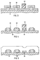
- FIGS. 1 to 4 represent purely schematic steps through successive manufacturing stages of semiconductor circuits. Identical features are provided with the same reference symbols in the figures.
- Printed conductors 20 made of metal, such as aluminum, or doped polysilicon (FIG. 1).
- the surface is then covered with a dielectric layer 30 of layer thickness d from e.g. SiO2 or phosphor silicate glass coated.
- the separation takes place e.g. by CVD (Fig. 2).
- a photoresist layer is now applied over the entire area and structured in a conventional manner to form the photomask 40, in such a way that it partially covers the layer 30 in the region between the conductor tracks 20.
- the minimum distance of the photomask 40 to the interconnects 20 is limited by technologically predetermined parameters such as layer thicknesses, adjustment accuracy of the exposure apparatus, optical properties of the tracks to be planarized, resolving power of the exposure machine for the photomask 40, etc. In practice, however, it is neither necessary nor desirable to work with minimum distances. Where the distances between conductor tracks 20 are too small, there is no photomask 40 (FIG. 3). These are areas in which the distance between the conductor tracks 20 is greater than a multiple of the thickness of the dielectric layer 30, and this includes the adjustment tolerances and the photo technology.
- the layer 30 is removed by anisotropic etching (FIG. 4).
- Spacers 35 remain on the edge of the conductor tracks 20, which represent a local planarization of the conductor track plane or correct undercut flanks of the conductor tracks 20, if necessary.
- the dielectric pieces 36 hidden under the photomask remain.
- the photomask 40 is removed and the planarization is continued in a conventional manner, so that the structure shown in FIG. 5 is obtained.
- a thin dielectric layer 31 can be applied for pre-planarization prior to the deposition of the dielectric layer 30 from e.g. Phosphorus silicate glass using the SOG method (not shown).
- a disadvantage of the method according to the invention is that an additional mask process has to be introduced. This contrasts with the fact that a reliable manufacturing process can only be feasible with this method. This applies in particular to circuits with non-periodic conductor track structures.
- this mask process is not critical if the additional dielectric pieces come sufficiently far from the structures to be leveled.
- the spacers on the conductor tracks created by the method contribute to the local planarization of the topography. They are part of the planarizations that are usually used.
Abstract
Verfahren zur globalen Planarisierung von Oberflächen integrierter Halbleiterschaltungen mit Leiterbahnen (20) auf der Oberfläche bei dem eine aus einem Dielektrikum bestehende Hilfsschicht (30) zurückgeätzt wird unter Freilegung der Leiterbahnen und der Oberfläche des Trägerkörpers (10). Wobei auf den Seiten der Leiterbahnen (20) Spacer (35) und unter der Photolackmaske (40) Dielektrikumstücke (36) entstehen. Anschliessend wird die Photomaske (40) abgetragen und die Planarisierung fortgesetzt. <IMAGE>Method for the global planarization of surfaces of integrated semiconductor circuits with conductor tracks (20) on the surface, in which an auxiliary layer (30) consisting of a dielectric is etched back while exposing the conductor tracks and the surface of the carrier body (10). Spacers (35) are formed on the sides of the conductor tracks (20) and dielectric pieces (36) are formed under the photoresist mask (40). The photomask (40) is then removed and the planarization is continued. <IMAGE>
Description
Die Erfindung betrifft ein Verfahren nach dem Oberbegriff des Anspruchs 1.The invention relates to a method according to the preamble of claim 1.
Ein ähnliches Verfahren ist beispielsweise aus EP 0 416 165 bekannt. Bei diesem Verfahren wird zunächst eine aus Siliziumdioxyd bestehende lokal planarisierte Isolationsschicht bestimmter Dicke auf der einzuebnenden strukturierten Schicht aufgebracht. Daraufhin werden als Hilfsebene invers zur darunterliegenden strukturierten Ebene Photolackstrukturen erzeugt. Eine weitere guthaftende und einzuebnende Hilfsschicht wird aufgebracht und der ganze Aufbau einer anisotropen Ätzung unterworfen. Dabei werden praktisch alle Hilfsschichten und die einzuebnende Schicht geätzt. Etwaige nach dem Rückätzen verbleibende Reste der Photolackstruktur werden abgelöst.A similar method is known for example from EP 0 416 165. In this method, a locally planarized insulation layer of a certain thickness consisting of silicon dioxide is first applied to the structured layer to be leveled. Thereupon, photoresist structures are generated as an auxiliary level inverse to the underlying structured level. Another well-adhering and leveling auxiliary layer is applied and the entire structure is subjected to anisotropic etching. Practically all auxiliary layers and the layer to be leveled are etched. Any residues of the photoresist structure remaining after the etching back are removed.
Bei der gegenwärtigen Tendenz zur Verkleinerung der Strukturen und der damit verbundenen Forderung nach Erhöhung des optischen Auflösungsvermögens der Belichtungsmaschinen können topographische Höhenschwankungen auf den Halbleiterschaltungen immer weniger hingenommen werden, weil mit zunehmender numerischer Apertur der Beschichtungsmaschinen deren Tiefenschärfe nicht mehr ausreicht, d.h. es zu einem Verlust an Tiefenschärfe kommt. Dadurch können beim Photoprozeß unerwünschte Photolackreste zurückbleiben. Mit der Zahl der Verdrahtungsebenen addieren sich zwangsläufig auch derartige Probleme. Große Schichtdicken machen sich ebenfalls nachteilig bemerkbar, außerdem kann man wiederum bei mehreren Verdrahtungsebenen dieselben nicht beliebig verkleinern.With the current tendency to reduce the size of the structures and the associated demand for increasing the optical resolution of the exposure machines, topographic fluctuations in height on the semiconductor circuits can be accepted less and less because the increasing the numerical aperture of the coating machines, the depth of field of which is no longer sufficient, i.e. there is a loss Selective focus is coming. As a result, unwanted photoresist residues can remain in the photoprocess. Such problems inevitably add up with the number of wiring levels. Large layer thicknesses also have a disadvantageous effect; moreover, the same cannot be reduced arbitrarily if there are several wiring levels.
Man kennt sogenannte lokale Planarisierungen, das sind Prozesse, bei denen z.B. eine Glasschicht in einem Temperschritt zum Fließen gebracht wird oder Prozesse, bei denen die Glasschicht zunächst abgeschieden und anschließend anisotrop rückgeätzt wird.So-called local planarizations are known, these are processes in which e.g. a glass layer is made to flow in a tempering step or processes in which the glass layer is first deposited and then anisotropically etched back.
Daneben gibt es auch noch andere globale Planarisierungsmethoden, z.B. mechanisches Schleifen von Oxydschichten. Nachteilig ist dabei, daß man nicht nur eine zusätzliche Schleifeinrichtung benötigt, sondern auch, daß dabei Steppermarken eingeebnet werden. Eine Alternative hierzu bildet das eingangs genannte Verfahren.There are also other global planarization methods, e.g. mechanical grinding of oxide layers. The disadvantage here is that you not only need an additional grinding device, but also that stepper marks are leveled. An alternative to this is the method mentioned at the beginning.
Aufgabe der Erfindung ist es, die Nachteile der geschilderten Prozesse zu vermeiden und eine vereinfachte Schrittfolge gegenüber dem Bekannten zur globalen Planarisierung unter Verwendung von herkömmlichen, fertigungstechnisch bewährten Verfahren und Vorrichtungen anzugeben.The object of the invention is to avoid the disadvantages of the processes described and to provide a simplified sequence of steps compared to the known method for global planarization using conventional methods and devices which have been tried and tested in production technology.
Die Aufgabe wird durch die in Anspruch 1 angegebene Erfindung gelöst, zweckmäßige Ausgestaltungen sind in den Unteransprüchen gekennzeichent.The object is achieved by the invention specified in claim 1, expedient refinements are characterized in the subclaims.
Anhand der Figuren 1 bis 4, die rein schematisch Schritte durch aufeinanderfolgende Herstellungsstufen von Halbleiterschaltungen darstellen, soll die Erfindung erläutert werden. Gleiche Merkmale sind in den Figuren mit gleichen Bezugszeichen versehen.The invention is to be explained on the basis of FIGS. 1 to 4, which represent purely schematic steps through successive manufacturing stages of semiconductor circuits. Identical features are provided with the same reference symbols in the figures.
Ausgehend von einem Halbleiterkörper 10 mit darin enthaltenen, nicht eingezeichneten und nach herkömmlichen Verfahren hergestellten Strukturen eines Halbleiterbauelements werden auf der Oberfläche des. Halbleiterkörpers 10 an den erforderlichen Stellen Leiterbahnen 20 aus Metall, wie z.B. Aluminium, oder dotiertem Polysilizium aufgebracht (Fig. 1).Proceeding from a
Die Oberfläche wird anschließend mit einer Dielektrikumsschicht 30 der Schichtdicke d aus z.B. SiO2 oder Phosphorsilikatglas überzogen. Die Abscheidung erfolgt dabei z.B. durch CVD (Fig. 2).The surface is then covered with a
Als nächster Schritt wird nun eine Photolackschicht flächendeckend aufgebracht und unter Ausbildung der Photomaske 40 nach herkömlicher Weise strukturiert, und zwar dergestalt, daß sie die Schicht 30 im Bereich zwischen den Leiterbahnen 20 teilweise bedeckt. Der Minimalabstand der Photomaske 40 zu den Leitbahnen 20 ist durch technologisch vorgegebene Parameter wie Schichtdicken, Justiergenauigkeit der Belichtungsapparaturen, optische Eigenschaften der zu planarisierenden Bahnen, Auflösungsvermögen der Belichtungsmaschine für die Photomaske 40 usw. begrenzt. In praxi ist es jedoch weder notwendig noch wünschenswert, mit Minimalabständen zu arbeiten. Dort, wo die Abstände zwischen Leiterbahnen 20 zu klein sind, gibt es keine Photomaske 40 (Fig. 3). Dies sind Bereiche, in denen der Anstand zwischen den Leiterbahnen 20 größer ist als das Mehrfache der Dicke der Dielektrikumsschicht 30, und zwar unter Einbeziehung der Justiertoleranzen und der Phototechnik.As the next step, a photoresist layer is now applied over the entire area and structured in a conventional manner to form the
Nun wird durch anisotrope Ätzung die Schicht 30 abgetragen (Fig. 4). Es verbleiben am Rande der Leiterbahnen 20 Spacer 35, die eine lokale Planarisierung der Leiterbahnebene darstellen bzw. ggf. unterschnittene Flanken der Leiterbahnen 20 korrigieren. Außerdem verbleiben die unter der Photomaske verborgenen Dielektrikumsstücke 36. Anschließend wird die Photomaske 40 abgetragen und die Planarisierung in konventioneller Weise fortgesetzt, so daß man die in Fig. 5 gezeigte Struktur erhält.Now the
Zur Unterstützung der angestrebten globalen Planarisierung kann vor der Abscheidung der Dielektrikumsschicht 30 eine dünne Dielektrikumsschicht 31 zur Vorplanarisierung aufgebracht werden aus z.B. Phosphorsilikatglas mittels SOG-Verfahren (nicht gezeigt).To support the desired global planarization, a thin dielectric layer 31 can be applied for pre-planarization prior to the deposition of the
Nachteilig bei dem erfindungsgemäßen Verfahren ist, daß ein zusätzlicher Maskenprozeß eingeführt werden muß. Dem steht gegenüber, daß mit diesem Verfahren u.U. ein zuverlässiger Herstellungsprozeß erst führbar ist. Dies gilt insbesondere bei Schaltungen mit nicht periodischen Leiterbahnstrukturen. Außerdem ist dieser Maskenprozeß unkritisch, wenn die zusätzlichen Dielektrikumsstücke hinreichend weit von den einzuebnenden Strukturen zu liegen kommen.
Die durch das Verfahren entstehenden Spacer an den Leiterbahnen tragen zur lokalen Planarisierung der Topographie bei. Sie sind an sich schon Bestandteil üblicherweise eingesetzter Planarisierungen.A disadvantage of the method according to the invention is that an additional mask process has to be introduced. This contrasts with the fact that a reliable manufacturing process can only be feasible with this method. This applies in particular to circuits with non-periodic conductor track structures. In addition, this mask process is not critical if the additional dielectric pieces come sufficiently far from the structures to be leveled.
The spacers on the conductor tracks created by the method contribute to the local planarization of the topography. They are part of the planarizations that are usually used.
Weiterhin entsteht kein zusätzlicher Aufwand im Schaltungsentwurf, weil sich die Zusatzmaske aus dem entsprechenden Verdrahtungslayout mit einem entsprechenden Rechnerprogramm ableiten läßt.Furthermore, there is no additional effort in the circuit design because the additional mask can be derived from the corresponding wiring layout with a corresponding computer program.
Claims (4)
Applications Claiming Priority (2)
| Application Number | Priority Date | Filing Date | Title |
|---|---|---|---|
| DE4239075A DE4239075C1 (en) | 1992-11-20 | 1992-11-20 | Process for the global planarization of surfaces of integrated semiconductor circuits |
| DE4239075 | 1992-11-20 |
Publications (2)
| Publication Number | Publication Date |
|---|---|
| EP0599074A1 true EP0599074A1 (en) | 1994-06-01 |
| EP0599074B1 EP0599074B1 (en) | 1999-04-21 |
Family
ID=6473289
Family Applications (1)
| Application Number | Title | Priority Date | Filing Date |
|---|---|---|---|
| EP93117463A Expired - Lifetime EP0599074B1 (en) | 1992-11-20 | 1993-10-28 | Method for the global planarization of surfaces of integrated semiconductor circuits |
Country Status (4)
| Country | Link |
|---|---|
| US (1) | US5445998A (en) |
| EP (1) | EP0599074B1 (en) |
| JP (1) | JPH076997A (en) |
| DE (2) | DE4239075C1 (en) |
Families Citing this family (7)
| Publication number | Priority date | Publication date | Assignee | Title |
|---|---|---|---|---|
| JP2926864B2 (en) * | 1990-04-12 | 1999-07-28 | ソニー株式会社 | Copper-based metal film etching method |
| US5840623A (en) * | 1995-10-04 | 1998-11-24 | Advanced Micro Devices, Inc. | Efficient and economical method of planarization of multilevel metallization structures in integrated circuits using CMP |
| JPH10112531A (en) * | 1996-08-13 | 1998-04-28 | Hitachi Ltd | Manufacture of semiconductor integrated circuit device |
| KR100481981B1 (en) * | 1997-12-29 | 2005-06-17 | 매그나칩 반도체 유한회사 | Interlayer insulating film formation method of semiconductor device |
| US6208004B1 (en) * | 1998-08-19 | 2001-03-27 | Philips Semiconductor, Inc. | Semiconductor device with high-temperature-stable gate electrode for sub-micron applications and fabrication thereof |
| US6448629B2 (en) | 1999-07-29 | 2002-09-10 | International Business Machines Corporation | Semiconductor device and method of making same |
| US7097788B2 (en) * | 2003-06-30 | 2006-08-29 | The Board Of Trustees Of The University Of Illinois | Conducting inks |
Citations (4)
| Publication number | Priority date | Publication date | Assignee | Title |
|---|---|---|---|---|
| EP0084635A2 (en) * | 1981-12-30 | 1983-08-03 | International Business Machines Corporation | Method of forming a wide deep dielectric filled isolation trench in the surface of a silicon semiconductor substrate |
| US4634496A (en) * | 1984-11-15 | 1987-01-06 | Kabushiki Kaisha Toshiba | Method for planarizing the surface of an interlayer insulating film in a semiconductor device |
| JPH0215624A (en) * | 1988-03-24 | 1990-01-19 | Motorola Inc | Method of levelling semiconductor device |
| EP0405850A2 (en) * | 1989-06-30 | 1991-01-02 | AT&T Corp. | Dielectric formation process and devices produced thereby |
Family Cites Families (8)
| Publication number | Priority date | Publication date | Assignee | Title |
|---|---|---|---|---|
| US4389281A (en) * | 1980-12-16 | 1983-06-21 | International Business Machines Corporation | Method of planarizing silicon dioxide in semiconductor devices |
| US4505029A (en) * | 1981-03-23 | 1985-03-19 | General Electric Company | Semiconductor device with built-up low resistance contact |
| US4662064A (en) * | 1985-08-05 | 1987-05-05 | Rca Corporation | Method of forming multi-level metallization |
| US4962060A (en) * | 1987-03-10 | 1990-10-09 | Advanced Micro Devices, Inc. | Making a high speed interconnect system with refractory non-dogbone contacts and an active electromigration suppression mechanism |
| GB2211348A (en) * | 1987-10-16 | 1989-06-28 | Philips Nv | A method of forming an interconnection between conductive levels |
| ATE115770T1 (en) * | 1989-09-08 | 1994-12-15 | Siemens Ag | PROCESS FOR GLOBAL PLANARISATION OF SURFACES FOR SEMICONDUCTOR INTEGRATED CIRCUITS. |
| US5229325A (en) * | 1991-01-31 | 1993-07-20 | Samsung Electronics Co., Ltd. | Method for forming metal wirings of semiconductor device |
| US5262352A (en) * | 1992-08-31 | 1993-11-16 | Motorola, Inc. | Method for forming an interconnection structure for conductive layers |
-
1992
- 1992-11-20 DE DE4239075A patent/DE4239075C1/en not_active Expired - Fee Related
-
1993
- 1993-10-28 EP EP93117463A patent/EP0599074B1/en not_active Expired - Lifetime
- 1993-10-28 DE DE59309525T patent/DE59309525D1/en not_active Expired - Fee Related
- 1993-11-17 US US08/154,670 patent/US5445998A/en not_active Expired - Fee Related
- 1993-11-22 JP JP5292242A patent/JPH076997A/en active Pending
Patent Citations (4)
| Publication number | Priority date | Publication date | Assignee | Title |
|---|---|---|---|---|
| EP0084635A2 (en) * | 1981-12-30 | 1983-08-03 | International Business Machines Corporation | Method of forming a wide deep dielectric filled isolation trench in the surface of a silicon semiconductor substrate |
| US4634496A (en) * | 1984-11-15 | 1987-01-06 | Kabushiki Kaisha Toshiba | Method for planarizing the surface of an interlayer insulating film in a semiconductor device |
| JPH0215624A (en) * | 1988-03-24 | 1990-01-19 | Motorola Inc | Method of levelling semiconductor device |
| EP0405850A2 (en) * | 1989-06-30 | 1991-01-02 | AT&T Corp. | Dielectric formation process and devices produced thereby |
Non-Patent Citations (1)
| Title |
|---|
| CHEMICAL PATENTS INDEX, DOCUMENTATION ABSTRACTS JOURNAL Section EI Week 9009, Derwent World Patents Index; Class U, AN 90-063004 * |
Also Published As
| Publication number | Publication date |
|---|---|
| US5445998A (en) | 1995-08-29 |
| EP0599074B1 (en) | 1999-04-21 |
| JPH076997A (en) | 1995-01-10 |
| DE4239075C1 (en) | 1994-04-07 |
| DE59309525D1 (en) | 1999-05-27 |
Similar Documents
| Publication | Publication Date | Title |
|---|---|---|
| DE3203898C2 (en) | ||
| DE4434230A1 (en) | Chemical-mechanical polishing process for leveling insulating layers | |
| DE112009001476T5 (en) | Process for producing semiconductor structures and semiconductor structures obtained by such processes | |
| DE10245179A1 (en) | Integrated circuit comprises first lines on first plane, and second lines on second plane | |
| DE102007026879A1 (en) | Method for producing a structure on or in a substrate, imaging layer for producing sub-lithographic structures, method for inverting a sub-lithographic pattern, device obtainable by producing a structure | |
| DE10154820B4 (en) | Method for producing a mask for semiconductor structures | |
| EP0599074B1 (en) | Method for the global planarization of surfaces of integrated semiconductor circuits | |
| DE4232821C2 (en) | Process for producing a finely structured semiconductor component | |
| EP1303880B1 (en) | Method for applying adjustment marks on a semiconductor disk | |
| EP0105189B1 (en) | Method of producing metal electrodes of diversing thiekness for semiconductor devices, especially for power semiconductor devices such as thyristors | |
| DE19719909A1 (en) | Dual damascene process for integrated circuits | |
| DE10130824C2 (en) | Repair method for a dielectric film with a hole defect on a substrate | |
| DE10200678A1 (en) | Process for processing a substrate to form a structure | |
| DE10239218A1 (en) | Method of manufacturing a semiconductor device and its construction | |
| DE3421127A1 (en) | METHOD FOR PRODUCING A SEMICONDUCTOR ARRANGEMENT | |
| EP0931439B1 (en) | Method for building at least two wiring levels on electrically insulated supports | |
| DE10259322B4 (en) | A method of forming an alignment mark in an opaque layer on a substrate | |
| DE19622415A1 (en) | CMOS semiconductor structure and method of manufacturing the same | |
| DE10312202B4 (en) | Method for producing an etching mask on a microstructure, in particular a semiconductor structure with trench capacitors, and corresponding use of the etching mask | |
| DE2703473C2 (en) | ||
| DE10128481B4 (en) | Process for etching a substrate | |
| DE19935130C1 (en) | Method for producing a contact hole for a semiconductor memory component | |
| DE102006030265B4 (en) | A method for improving the planarity of a surface topography in a microstructure | |
| EP0764983B1 (en) | Semiconductor device and method of manufacturing the same | |
| WO2002089202A2 (en) | Method for the production of an integrated circuit |
Legal Events
| Date | Code | Title | Description |
|---|---|---|---|
| PUAI | Public reference made under article 153(3) epc to a published international application that has entered the european phase |
Free format text: ORIGINAL CODE: 0009012 |
|
| AK | Designated contracting states |
Kind code of ref document: A1 Designated state(s): DE FR NL |
|
| 17P | Request for examination filed |
Effective date: 19941130 |
|
| 17Q | First examination report despatched |
Effective date: 19960515 |
|
| RAP1 | Party data changed (applicant data changed or rights of an application transferred) |
Owner name: MICRONAS INTERMETALL GMBH |
|
| GRAG | Despatch of communication of intention to grant |
Free format text: ORIGINAL CODE: EPIDOS AGRA |
|
| GRAG | Despatch of communication of intention to grant |
Free format text: ORIGINAL CODE: EPIDOS AGRA |
|
| GRAH | Despatch of communication of intention to grant a patent |
Free format text: ORIGINAL CODE: EPIDOS IGRA |
|
| GRAH | Despatch of communication of intention to grant a patent |
Free format text: ORIGINAL CODE: EPIDOS IGRA |
|
| GRAA | (expected) grant |
Free format text: ORIGINAL CODE: 0009210 |
|
| AK | Designated contracting states |
Kind code of ref document: B1 Designated state(s): DE FR NL |
|
| REF | Corresponds to: |
Ref document number: 59309525 Country of ref document: DE Date of ref document: 19990527 |
|
| ET | Fr: translation filed | ||
| PLBE | No opposition filed within time limit |
Free format text: ORIGINAL CODE: 0009261 |
|
| STAA | Information on the status of an ep patent application or granted ep patent |
Free format text: STATUS: NO OPPOSITION FILED WITHIN TIME LIMIT |
|
| 26N | No opposition filed | ||
| PGFP | Annual fee paid to national office [announced via postgrant information from national office to epo] |
Ref country code: FR Payment date: 20011002 Year of fee payment: 9 |
|
| PGFP | Annual fee paid to national office [announced via postgrant information from national office to epo] |
Ref country code: DE Payment date: 20011004 Year of fee payment: 9 |
|
| PGFP | Annual fee paid to national office [announced via postgrant information from national office to epo] |
Ref country code: NL Payment date: 20011009 Year of fee payment: 9 |
|
| PG25 | Lapsed in a contracting state [announced via postgrant information from national office to epo] |
Ref country code: NL Free format text: LAPSE BECAUSE OF NON-PAYMENT OF DUE FEES Effective date: 20030501 Ref country code: DE Free format text: LAPSE BECAUSE OF NON-PAYMENT OF DUE FEES Effective date: 20030501 |
|
| PG25 | Lapsed in a contracting state [announced via postgrant information from national office to epo] |
Ref country code: FR Free format text: LAPSE BECAUSE OF NON-PAYMENT OF DUE FEES Effective date: 20030630 |
|
| NLV4 | Nl: lapsed or anulled due to non-payment of the annual fee |
Effective date: 20030501 |
|
| REG | Reference to a national code |
Ref country code: FR Ref legal event code: ST |