EP0596771B1 - Anordnung zum elektrischen Verbinden von gedruckten Leiterplatten, von denen mindestens eine biegsam ist - Google Patents
Anordnung zum elektrischen Verbinden von gedruckten Leiterplatten, von denen mindestens eine biegsam ist Download PDFInfo
- Publication number
- EP0596771B1 EP0596771B1 EP93402616A EP93402616A EP0596771B1 EP 0596771 B1 EP0596771 B1 EP 0596771B1 EP 93402616 A EP93402616 A EP 93402616A EP 93402616 A EP93402616 A EP 93402616A EP 0596771 B1 EP0596771 B1 EP 0596771B1
- Authority
- EP
- European Patent Office
- Prior art keywords
- supports
- electrical connection
- contacts
- housing
- connection device
- Prior art date
- Legal status (The legal status is an assumption and is not a legal conclusion. Google has not performed a legal analysis and makes no representation as to the accuracy of the status listed.)
- Expired - Lifetime
Links
Images

Classifications
-
- H—ELECTRICITY
- H01—ELECTRIC ELEMENTS
- H01R—ELECTRICALLY-CONDUCTIVE CONNECTIONS; STRUCTURAL ASSOCIATIONS OF A PLURALITY OF MUTUALLY-INSULATED ELECTRICAL CONNECTING ELEMENTS; COUPLING DEVICES; CURRENT COLLECTORS
- H01R13/00—Details of coupling devices of the kinds covered by groups H01R12/70 or H01R24/00 - H01R33/00
- H01R13/02—Contact members
- H01R13/22—Contacts for co-operating by abutting
- H01R13/24—Contacts for co-operating by abutting resilient; resiliently-mounted
- H01R13/2464—Contacts for co-operating by abutting resilient; resiliently-mounted characterized by the contact point
- H01R13/2471—Contacts for co-operating by abutting resilient; resiliently-mounted characterized by the contact point pin shaped
-
- H—ELECTRICITY
- H01—ELECTRIC ELEMENTS
- H01R—ELECTRICALLY-CONDUCTIVE CONNECTIONS; STRUCTURAL ASSOCIATIONS OF A PLURALITY OF MUTUALLY-INSULATED ELECTRICAL CONNECTING ELEMENTS; COUPLING DEVICES; CURRENT COLLECTORS
- H01R12/00—Structural associations of a plurality of mutually-insulated electrical connecting elements, specially adapted for printed circuits, e.g. printed circuit boards [PCB], flat or ribbon cables, or like generally planar structures, e.g. terminal strips, terminal blocks; Coupling devices specially adapted for printed circuits, flat or ribbon cables, or like generally planar structures; Terminals specially adapted for contact with, or insertion into, printed circuits, flat or ribbon cables, or like generally planar structures
- H01R12/70—Coupling devices
- H01R12/77—Coupling devices for flexible printed circuits, flat or ribbon cables or like structures
- H01R12/78—Coupling devices for flexible printed circuits, flat or ribbon cables or like structures connecting to other flexible printed circuits, flat or ribbon cables or like structures
-
- H—ELECTRICITY
- H01—ELECTRIC ELEMENTS
- H01R—ELECTRICALLY-CONDUCTIVE CONNECTIONS; STRUCTURAL ASSOCIATIONS OF A PLURALITY OF MUTUALLY-INSULATED ELECTRICAL CONNECTING ELEMENTS; COUPLING DEVICES; CURRENT COLLECTORS
- H01R12/00—Structural associations of a plurality of mutually-insulated electrical connecting elements, specially adapted for printed circuits, e.g. printed circuit boards [PCB], flat or ribbon cables, or like generally planar structures, e.g. terminal strips, terminal blocks; Coupling devices specially adapted for printed circuits, flat or ribbon cables, or like generally planar structures; Terminals specially adapted for contact with, or insertion into, printed circuits, flat or ribbon cables, or like generally planar structures
- H01R12/70—Coupling devices
- H01R12/77—Coupling devices for flexible printed circuits, flat or ribbon cables or like structures
- H01R12/79—Coupling devices for flexible printed circuits, flat or ribbon cables or like structures connecting to rigid printed circuits or like structures
-
- H—ELECTRICITY
- H05—ELECTRIC TECHNIQUES NOT OTHERWISE PROVIDED FOR
- H05K—PRINTED CIRCUITS; CASINGS OR CONSTRUCTIONAL DETAILS OF ELECTRIC APPARATUS; MANUFACTURE OF ASSEMBLAGES OF ELECTRICAL COMPONENTS
- H05K3/00—Apparatus or processes for manufacturing printed circuits
- H05K3/36—Assembling printed circuits with other printed circuits
- H05K3/361—Assembling flexible printed circuits with other printed circuits
- H05K3/365—Assembling flexible printed circuits with other printed circuits by abutting, i.e. without alloying process
Definitions
- the present invention relates to electrical connection devices for insulating supports, carrying printed circuits, at least one of which is flexible.
- connectors are used provided with female plugs, into which are plugged male plugs arranged on said supports.
- female plugs into which are plugged male plugs arranged on said supports.
- the contacting being done by force, there is a wear of the plugs decreasing the efficiency of the connection after a certain number of plugging and unplugging operations.
- the replacement of said plugs is delicate and very expensive, and the same is true for the implementation of a surface protection against wear, such as for example the covering of the plugs with a metal resistant to 'wear.
- the object of the present invention is to remedy these drawbacks and relates to a connection device which does not involve any insertion friction, when the supports, carrying printed circuits, are brought into electrical contact.
- the connection device according to the present invention is specially adapted for a connection, for which at least one of the supports is flexible.
- connection device intended for connecting insulating supports, carrying printed circuits, at least one of which is flexible, each of said supports being provided on one of its faces with contacts intended for connection, is remarkable.
- said contacts protrude relative to the face of said supports which carries them and in that said connection device electric comprises a layer of elastically deformable material, capable of exerting pressure on the face not provided with contacts of said flexible support, in order to press it against at least one other of said supports, which is in abutment against a rigid element, so that each contact, intended to be connected, of said flexible support is brought into contact with a contact, intended to be connected, of another of said supports.
- the present invention therefore eliminates the problems due to insertion friction, by creating a connection device in which the electrical connection does not result from the insertion of an element into another element, but from the simple contacting of two elements, in this case the contacting of two contacts arranged on the faces of the supports to be connected.
- the supports to be connected are arranged opposite one another so that each contact, intended for connection, of one of said supports, is facing a contact, intended for connection, of another of said supports.
- the electrical connection device then allows, thanks to said layer of material elastically deformable, to exert pressure on the face not provided with contacts of the flexible support, opposite the contact which is less protruding, such that said flexible support deforms locally in order to fill said spacing and ensure contacting of said less protruding contact with his associated contact.
- the pressure applied is thus distributed along the flexible support so as to obtain an adequate pressure at the level of each contact to allow the electrical connection of all the protruding contacts, intended for connection, by compensating for any height inequalities of said contacts.
- variable spacing between the ends of associated contacts could also be due to a lack of flatness of the surface provided with contacts of one of said supports.
- said electrical connection device comprises a pressure plate which carries said layer of elastically deformable material by its face which is not in contact with the flexible support and which is, for example, subjected to the pressure of a spring, which provides the contact pressure.
- said electrical connection device comprises, on the one hand, a housing containing said pressure plate and said spring and releasing said layer of elastically deformable material, and, on the other hand, a rigid cover which can be coupled to said housing opposite said layer of elastically deformable material.
- said electrical connection device may be provided with complementary guiding means, for example positioning pins arranged on said housing and recesses made in said cover, guiding the movements of approaching and moving said cover away from said housing.
- Said positioning pins can, moreover, be intended to favor the positioning of the supports on the housing, said supports having holes and being placed by means of the latter on said positioning pins.
- said housing and said rigid cover can also be provided with a screw fixing system facilitating the installation and maintenance of said connection device.
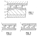
- Figure 1 is an enlarged schematic sectional view illustrating the electrical connection between a flexible support and a rigid support, according to the invention.
- Figure 2 shows partially in section two supports provided with contacts arranged opposite one another.
- FIG. 3 also shows in partial section two supports arranged opposite one another, one of which has a surface recess.
- FIG. 4 is a cross-sectional view of an embodiment of the present invention, along the line IV-IV of FIG. 5.
- Figure 5 is a sectional view along the line V-V in Figure 4.
- the electrical connection device in accordance with the present invention and shown diagrammatically and partially in FIG. 1, is intended to electrically connect insulating supports 1 and 2, carrying printed circuits, and provided with contacts 3, 4, 5, 6, 7 and 8 which project from the surface of said supports. Said contacts have the same arrangement on each of said supports 1 and 2, so that each contact 3, 5, 7 of support 1 can be brought opposite a contact 4, 6, 8 of support 2, when the two supports are arranged one opposite the other.
- the support 1 is supported on a rigid element 9.
- the support 2 is pressed against said support 1 by a layer 10 of elastically deformable material, for example an elastomer, subjected to the pressure of a pressure plate 11.
- Said pressed support 2 is flexible, while the other support 1, which bears on the rigid element 9 and which does not therefore undergo any deformation, even if it is flexible, can be either flexible or rigid.
- the contact 5 is less protruding than the neighboring contacts 3 and 7.
- the contacts 3 and 7 respectively come into contact contacts 4 and 8 associated with them, while contact 5 is not protruding enough to reach contact 6 associated with it.
- the distance separating two contacts is even greater when each of the two associated contacts is less prominent than its neighbors.
- the contacting of the contacts 5 and 6 is obtained by deformation of the flexible support 2 under the action of the layer 10 of elastically deformable material.
- Said flexible support 2 reproduces, in fact, the shape of the pressure surface 12 of said layer 10. The latter, when pressed against the flexible support 2, acquires, thanks to its elasticity, a thickness which varies according to the location of the contacts of the flexible support which are supported on their associated contacts.
- the pressure surface 12 and the flexible support 2 have a configuration such that all the contacts of the flexible support 2 bear against the contacts of the support 1 which are associated with them.
- the undesirable spacing between two associated contacts, in the close contact position of said supports 1 and 2 can come, either as shown in FIG. 2 and mentioned above, from a lower height of at least one of the contacts, either as shown in Figure 3, a lack of flatness of the surface of the support 1 provided with contacts, a contact 5 'then being in a recess of said surface.
- the contacts 3 ', 4', 5 ', 6', 7 'and 8' arranged on the supports 1 and 2 play the same role as the contacts 3, 4, 5, 6, 7 and 8 of Figure 2.
- the electrical connection device comprises a housing 22 and a rigid cover 9, which is capable of being fixed on said housing 22 using screws 23.
- Said electrical connection device also comprises a wavy leaf spring 24 housed in the housing 22, bearing against the bottom of the latter and pushing outward a pressure plate 11.
- Said pressure plate 11 is pushed by the spring 24 against stops 25 and 26, which are arranged on said housing 22, and which make it trapped in the housing 22.
- said pressure plate 11 is covered with a layer 10 of elastically deformable material which protrudes at the outside of the housing, between the stops 25 and 26.
- Said electrical connection device is intended to connect two supports 1 and 2 both provided, on one face of one of their ends, with protruding contacts such as those bearing the references 3 to 8 and 3 'to 8' of the figures 1 to 3.
- the ends provided with contacts of said supports 1 and 2 are arranged, face to face, on said housing 22, the support 2 which bears on the housing 22 and on the layer 10 of elastically deformable material being flexible, the other support 1 can be either rigid or flexible.
- Said supports 1 and 2 are placed on said housing 22 by means of projecting positioning pins 27 arranged on the pressure plate 11 and intended to be placed in holes 29 and 30, respectively provided on said supports 1 and 2
- the supports 1 and 2 are then in the same situation as in FIG. 1. They are, in fact, compressed between the rigid cover 9 and the layer 10 of elastically deformable material.
- the rigid cover 9 is screwed on, until the pressure exerted by said layer 10, under the action of the spring 24 and of the pressure plate 11, is sufficient to allow electrical connection between all of the associated pairs of contacts of the two supports 1 and 2.
Landscapes
- Engineering & Computer Science (AREA)
- Metallurgy (AREA)
- Manufacturing & Machinery (AREA)
- Microelectronics & Electronic Packaging (AREA)
- Coupling Device And Connection With Printed Circuit (AREA)
- Multi-Conductor Connections (AREA)
- Combinations Of Printed Boards (AREA)
Claims (9)
- Anordnung zum elektrischen Verbinden von gedruckten Leiterplatten, die jeweils auf einer Seite ihres entsprechenden isolierenden Trägers (1,2) Kontakte (3 bis 8, 3' bis 8') zur Verbindung haben,
dadurch gekennzeichnet, daß die Kontakte auf der Seite der Träger, auf der sie angeordnet sind, überstehen, dadurch, daß mindestens der isolierende Träger (2) einer der gedruckten Schaltungen biegsam ist, und dadurch, daß eine Schicht (10) aus einem elastisch verformbaren Material zur Ausübung eines Drucks auf die Seite ohne Kontakte des biegsamen Trägers (2) vorgesehen ist, so daß dieser gegen mindestens einen anderen Träger (1) gedrückt wird, der an einem starren Element (9) anliegt, so daß jeder zu verbindende Kontakt (4,6,8,4',6',8') des biegsamen Trägers (2) mit einem zu verbindenden Kontakt (3,5,7,3',5',7') eines anderen Trägers (1) in Kontakt gebracht wird. - Anordnung zum elektrischen Verbinden nach Anspruch 1,
dadurch gekennzeichnet, daß sich die Schicht (10) aus einem elastisch verformbaren Material auf einer starren Druckplatte (11) befindet. - Anordnung zum elektrischen Verbinden nach Anspruch 2,
dadurch gekennzeichnet, daß die starre Druckplatte (11) von einer Feder (24) beaufschlagt wird. - Anordnung zum elektrischen Verbinden nach einem der Ansprüche 1 bis 3,
dadurch gekennzeichnet, daß die Schicht (10) aus einem elastisch verformbaren Material aus einem Elastomer besteht. - Anordnung zum elektrischen Verbinden nach einem der Ansprüche 3 oder 4,
dadurch gekennzeichnet, daß sie einerseits ein Gehäuse (22) mit der starren Druckplatte (11) und der Feder (24), durch das die Schicht (10) aus einem elastisch verformbaren Material freigegeben wird, und andererseits einen starren Deckel (9) hat, der gegenüber der Schicht (10) aus einem elastisch verformbaren Material mit dem Gehäuse (22) gekoppelt werden kann. - Anordnung zum elektrischen Verbinden nach Anspruch 5,
dadurch gekennzeichnet, daß das Gehäuse (22) und der starre Deckel (9) zusätzliche Führungsmittel (27,28) haben, durch die die An- und Abstellbewegungen des starren Deckels (9) in Bezug auf das Gehäuse (22) gesteuert werden können. - Anordnung zum elektrischen Verbinden nach Anspruch 6,
dadurch gekennzeichnet, daß die zusätzlichen Führungsmittel (27,28) Positionierungsstifte (27) und Aussparungen (28) haben, die jeweils am Gehäuse (22) und am starren Deckel (9) vorgesehen sind. - Anordnung zum elektrischen Verbinden nach Anspruch 7,
dadurch gekennzeichnet, daß die Positionierungsstifte (27) durch Bohrungen (29) und (30) verlaufen, die in den isolierenden Trägern 1 bzw. 2 angeordnet sind, damit diese gegenüber dem Gehäuse (22) positioniert werden können. - Anordnung zum elektrischen Verbinden nach einem der Ansprüche 5 bis 8,
dadurch gekennzeichnet, daß das Gehäuse (22) und der starre Deckel (9) miteinander durch Schrauben (23) befestigt werden.
Applications Claiming Priority (2)
| Application Number | Priority Date | Filing Date | Title |
|---|---|---|---|
| FR9213201A FR2697684B1 (fr) | 1992-11-04 | 1992-11-04 | Dispositif de connexion électrique pour circuits imprimés dont au moins l'un est souple. |
| FR9213201 | 1992-11-04 |
Publications (3)
| Publication Number | Publication Date |
|---|---|
| EP0596771A2 EP0596771A2 (de) | 1994-05-11 |
| EP0596771A3 EP0596771A3 (de) | 1995-04-12 |
| EP0596771B1 true EP0596771B1 (de) | 1997-01-08 |
Family
ID=9435166
Family Applications (1)
| Application Number | Title | Priority Date | Filing Date |
|---|---|---|---|
| EP93402616A Expired - Lifetime EP0596771B1 (de) | 1992-11-04 | 1993-10-26 | Anordnung zum elektrischen Verbinden von gedruckten Leiterplatten, von denen mindestens eine biegsam ist |
Country Status (5)
| Country | Link |
|---|---|
| EP (1) | EP0596771B1 (de) |
| AT (1) | ATE147550T1 (de) |
| DE (1) | DE69307273T2 (de) |
| ES (1) | ES2098699T3 (de) |
| FR (1) | FR2697684B1 (de) |
Family Cites Families (4)
| Publication number | Priority date | Publication date | Assignee | Title |
|---|---|---|---|---|
| DE2234960C3 (de) * | 1971-11-26 | 1975-04-30 | Teledyne, Inc., Los Angeles, Calif. (V.St.A.) | Elektrischer Stecker |
| NL158033B (nl) * | 1974-02-27 | 1978-09-15 | Amp Inc | Verbetering van een elektrisch verbindingsorgaan voor het losneembaar verbinden van twee vaste contactdragers en werkwijze voor het vervaardigen van zulk een elektrisch verbindingsorgaan. |
| US4693529A (en) * | 1986-03-31 | 1987-09-15 | Amp Incorporated | Elastomeric mother-daughter board electrical connector |
| US5061192A (en) * | 1990-12-17 | 1991-10-29 | International Business Machines Corporation | High density connector |
-
1992
- 1992-11-04 FR FR9213201A patent/FR2697684B1/fr not_active Expired - Fee Related
-
1993
- 1993-10-26 DE DE69307273T patent/DE69307273T2/de not_active Expired - Fee Related
- 1993-10-26 EP EP93402616A patent/EP0596771B1/de not_active Expired - Lifetime
- 1993-10-26 AT AT93402616T patent/ATE147550T1/de not_active IP Right Cessation
- 1993-10-26 ES ES93402616T patent/ES2098699T3/es not_active Expired - Lifetime
Also Published As
| Publication number | Publication date |
|---|---|
| FR2697684B1 (fr) | 1995-01-06 |
| EP0596771A2 (de) | 1994-05-11 |
| ATE147550T1 (de) | 1997-01-15 |
| DE69307273T2 (de) | 1997-05-15 |
| FR2697684A1 (fr) | 1994-05-06 |
| EP0596771A3 (de) | 1995-04-12 |
| DE69307273D1 (de) | 1997-02-20 |
| ES2098699T3 (es) | 1997-05-01 |
Similar Documents
| Publication | Publication Date | Title |
|---|---|---|
| CA2034494C (fr) | Connecteur electrique pour le raccordement d'un cable multiconducteur blinde a un ensemble electrique place a l'interieur d'un chassis | |
| EP0807995B1 (de) | Anordnung zum Verbinden eines Koaxialkabels mit einer gedruckten Leiterplatte | |
| FR2495846A1 (fr) | Dispositif de connexion electrique a haute densite de contacts | |
| EP1028490A1 (de) | Koaxialverbinder zum Verbinden von zwei Leiterplatten | |
| FR2504316A1 (fr) | Contact electrique | |
| FR2722617A1 (fr) | Contacts electriques a ressort plein pour des connecteurs et des sondes electriques | |
| FR2756425A1 (fr) | Structure de connecteur electrique | |
| FR2566590A1 (fr) | Connecteur pour interconnecter des plaquettes de circuit imprime | |
| FR2542508A1 (fr) | Ensemble forme d'une plaquette de base a circuits imprimes sur laquelle est fixee de facon amovible une plaquette rapportee a circuits imprimes | |
| EP0401121A1 (de) | Verbindungszusammenbau für gedruckte Schaltungskarten | |
| EP0251869A1 (de) | Verbinder für Flachverbindung | |
| EP0596771B1 (de) | Anordnung zum elektrischen Verbinden von gedruckten Leiterplatten, von denen mindestens eine biegsam ist | |
| FR2642572A1 (fr) | Agencement pour realiser une connexion demontable entre des substrats | |
| FR2517482A1 (fr) | Dispositif de continuite de masse entre boitiers de connecteurs | |
| FR2799890A1 (fr) | Connecteur comportant des contacts shuntables et configurables | |
| GB2163012A (en) | Filtered electrical connectors | |
| EP0558407B1 (de) | Elektrischer Verbinder, versehen mit einer elektrischen Verbindung zwischen den entsprechenden Kontaktteilen | |
| EP0987793B1 (de) | Elektrischer Verbinder mit geringer Einsteckkraft insbesondere mit Kontaktmesser für flexible Schaltung | |
| EP1019864B1 (de) | Kartenleserverbindung mit elektrischen bürstenkontakten und damit ausgerüsteter leser | |
| EP0596770B1 (de) | Elektrische Kupplungsvorrichtung für gedruckte Schaltungen | |
| FR2696586A1 (fr) | Connecteur à diode/filtre. | |
| CA1201497A (fr) | Borne de raccordement pour carte a circuit imprime et appareil utilisant de telles bornes | |
| FR2764445A1 (fr) | Dispositif d'interconnexion par module(s) a fiches de connexion disposees lineairement et composants mis en oeuvre dans un tel dispositif | |
| FR2692407A1 (fr) | Dispositif de codage indexable hermaphrodite et connecteur l'utilisant. | |
| EP0517123B1 (de) | Abschirmvorrichtung für Verbinder |
Legal Events
| Date | Code | Title | Description |
|---|---|---|---|
| PUAI | Public reference made under article 153(3) epc to a published international application that has entered the european phase |
Free format text: ORIGINAL CODE: 0009012 |
|
| AK | Designated contracting states |
Kind code of ref document: A2 Designated state(s): AT BE CH DE DK ES GB IE IT LI NL SE |
|
| PUAL | Search report despatched |
Free format text: ORIGINAL CODE: 0009013 |
|
| AK | Designated contracting states |
Kind code of ref document: A3 Designated state(s): AT BE CH DE DK ES GB IE IT LI NL SE |
|
| 17P | Request for examination filed |
Effective date: 19950516 |
|
| 17Q | First examination report despatched |
Effective date: 19951004 |
|
| GRAG | Despatch of communication of intention to grant |
Free format text: ORIGINAL CODE: EPIDOS AGRA |
|
| GRAH | Despatch of communication of intention to grant a patent |
Free format text: ORIGINAL CODE: EPIDOS IGRA |
|
| GRAH | Despatch of communication of intention to grant a patent |
Free format text: ORIGINAL CODE: EPIDOS IGRA |
|
| GRAA | (expected) grant |
Free format text: ORIGINAL CODE: 0009210 |
|
| AK | Designated contracting states |
Kind code of ref document: B1 Designated state(s): AT BE CH DE DK ES GB IE IT LI NL SE |
|
| PG25 | Lapsed in a contracting state [announced via postgrant information from national office to epo] |
Ref country code: NL Free format text: LAPSE BECAUSE OF FAILURE TO SUBMIT A TRANSLATION OF THE DESCRIPTION OR TO PAY THE FEE WITHIN THE PRESCRIBED TIME-LIMIT Effective date: 19970108 Ref country code: DK Effective date: 19970108 Ref country code: AT Effective date: 19970108 |
|
| REF | Corresponds to: |
Ref document number: 147550 Country of ref document: AT Date of ref document: 19970115 Kind code of ref document: T |
|
| REG | Reference to a national code |
Ref country code: CH Ref legal event code: NV Representative=s name: JOHN P. MUNZINGER INGENIEUR-CONSEIL Ref country code: CH Ref legal event code: EP |
|
| GBT | Gb: translation of ep patent filed (gb section 77(6)(a)/1977) |
Effective date: 19970110 |
|
| REF | Corresponds to: |
Ref document number: 69307273 Country of ref document: DE Date of ref document: 19970220 |
|
| REG | Reference to a national code |
Ref country code: IE Ref legal event code: FG4D Free format text: 71441 |
|
| ITF | It: translation for a ep patent filed | ||
| REG | Reference to a national code |
Ref country code: ES Ref legal event code: FG2A Ref document number: 2098699 Country of ref document: ES Kind code of ref document: T3 |
|
| NLV1 | Nl: lapsed or annulled due to failure to fulfill the requirements of art. 29p and 29m of the patents act | ||
| PG25 | Lapsed in a contracting state [announced via postgrant information from national office to epo] |
Ref country code: SE Free format text: LAPSE BECAUSE OF NON-PAYMENT OF DUE FEES Effective date: 19971027 |
|
| PG25 | Lapsed in a contracting state [announced via postgrant information from national office to epo] |
Ref country code: LI Free format text: LAPSE BECAUSE OF NON-PAYMENT OF DUE FEES Effective date: 19971031 Ref country code: CH Free format text: LAPSE BECAUSE OF NON-PAYMENT OF DUE FEES Effective date: 19971031 |
|
| PLBE | No opposition filed within time limit |
Free format text: ORIGINAL CODE: 0009261 |
|
| STAA | Information on the status of an ep patent application or granted ep patent |
Free format text: STATUS: NO OPPOSITION FILED WITHIN TIME LIMIT |
|
| 26N | No opposition filed | ||
| PG25 | Lapsed in a contracting state [announced via postgrant information from national office to epo] |
Ref country code: IE Free format text: LAPSE BECAUSE OF NON-PAYMENT OF DUE FEES Effective date: 19980330 |
|
| REG | Reference to a national code |
Ref country code: IE Ref legal event code: FD4D Ref document number: 71441 Country of ref document: IE |
|
| REG | Reference to a national code |
Ref country code: CH Ref legal event code: PL |
|
| EUG | Se: european patent has lapsed |
Ref document number: 93402616.2 |
|
| PGFP | Annual fee paid to national office [announced via postgrant information from national office to epo] |
Ref country code: DE Payment date: 20010928 Year of fee payment: 9 |
|
| PGFP | Annual fee paid to national office [announced via postgrant information from national office to epo] |
Ref country code: BE Payment date: 20011009 Year of fee payment: 9 |
|
| PGFP | Annual fee paid to national office [announced via postgrant information from national office to epo] |
Ref country code: GB Payment date: 20011024 Year of fee payment: 9 |
|
| PGFP | Annual fee paid to national office [announced via postgrant information from national office to epo] |
Ref country code: ES Payment date: 20011026 Year of fee payment: 9 |
|
| REG | Reference to a national code |
Ref country code: GB Ref legal event code: IF02 |
|
| PG25 | Lapsed in a contracting state [announced via postgrant information from national office to epo] |
Ref country code: GB Free format text: LAPSE BECAUSE OF NON-PAYMENT OF DUE FEES Effective date: 20021026 |
|
| PG25 | Lapsed in a contracting state [announced via postgrant information from national office to epo] |
Ref country code: ES Free format text: LAPSE BECAUSE OF NON-PAYMENT OF DUE FEES Effective date: 20021027 |
|
| PG25 | Lapsed in a contracting state [announced via postgrant information from national office to epo] |
Ref country code: BE Free format text: LAPSE BECAUSE OF NON-PAYMENT OF DUE FEES Effective date: 20021031 |
|
| BERE | Be: lapsed |
Owner name: *AEROSPATIALE SOC. NATIONALE INDUSTRIELLE Effective date: 20021031 |
|
| PG25 | Lapsed in a contracting state [announced via postgrant information from national office to epo] |
Ref country code: DE Free format text: LAPSE BECAUSE OF NON-PAYMENT OF DUE FEES Effective date: 20030501 |
|
| GBPC | Gb: european patent ceased through non-payment of renewal fee | ||
| REG | Reference to a national code |
Ref country code: ES Ref legal event code: FD2A Effective date: 20031112 |
|
| PG25 | Lapsed in a contracting state [announced via postgrant information from national office to epo] |
Ref country code: IT Free format text: LAPSE BECAUSE OF NON-PAYMENT OF DUE FEES;WARNING: LAPSES OF ITALIAN PATENTS WITH EFFECTIVE DATE BEFORE 2007 MAY HAVE OCCURRED AT ANY TIME BEFORE 2007. THE CORRECT EFFECTIVE DATE MAY BE DIFFERENT FROM THE ONE RECORDED. Effective date: 20051026 |