EP0594352B1 - Schaltung zur Minimisierung der Spitzenleistung in einem Verstärker mit einer Vielzahl von Signalen unterschiedlicher Frequenzen - Google Patents
Schaltung zur Minimisierung der Spitzenleistung in einem Verstärker mit einer Vielzahl von Signalen unterschiedlicher Frequenzen Download PDFInfo
- Publication number
- EP0594352B1 EP0594352B1 EP93308164A EP93308164A EP0594352B1 EP 0594352 B1 EP0594352 B1 EP 0594352B1 EP 93308164 A EP93308164 A EP 93308164A EP 93308164 A EP93308164 A EP 93308164A EP 0594352 B1 EP0594352 B1 EP 0594352B1
- Authority
- EP
- European Patent Office
- Prior art keywords
- peak power
- signals
- amplifier system
- further including
- output
- Prior art date
- Legal status (The legal status is an assumption and is not a legal conclusion. Google has not performed a legal analysis and makes no representation as to the accuracy of the status listed.)
- Expired - Lifetime
Links
Images


Classifications
-
- H—ELECTRICITY
- H03—ELECTRONIC CIRCUITRY
- H03G—CONTROL OF AMPLIFICATION
- H03G3/00—Gain control in amplifiers or frequency changers
- H03G3/20—Automatic control
- H03G3/30—Automatic control in amplifiers having semiconductor devices
- H03G3/3036—Automatic control in amplifiers having semiconductor devices in high-frequency amplifiers or in frequency-changers
- H03G3/3042—Automatic control in amplifiers having semiconductor devices in high-frequency amplifiers or in frequency-changers in modulators, frequency-changers, transmitters or power amplifiers
-
- H—ELECTRICITY
- H03—ELECTRONIC CIRCUITRY
- H03F—AMPLIFIERS
- H03F1/00—Details of amplifiers with only discharge tubes, only semiconductor devices or only unspecified devices as amplifying elements
- H03F1/34—Negative-feedback-circuit arrangements with or without positive feedback
Definitions
- This invention relates to amplifier systems.
- the power signals of many channels are combined into a composite signal.
- This composite signal is split into many parallel paths and coupled to individual radio transmitters in each parallel path.
- the output radio transmission signals of the plurality of radio transmitters are combined and amplified in a single power amplifier. Individual signal peaks in each of the parallel paths may coincide and cause a composite peak power to occur at the single power amplifier that greatly exceeds its power handling capacity.
- the various radio channels are distributed in frequency with respect to each other in that each operates within a different frequency band. Simultaneous occurrence of individual signal peaks readily occur and hence the multi-channel signal is subject to power maximums where the peak power significantly exceeds the average power of the envelope due to constructive addition of the individual signal peaks.
- U.S. patent 4,064,464 discloses an amplifier system, including a power splitter for dividing an input signal into a plurality of channels and feeding each channel into a plurality of power amplifiers connected in parallel. The several output of the parallel connected power amplifiers are combined into a single output by a subsequent power combiner connected to the parallel outputs of the power amplifiers.
- the input to one of the paralleled amplifiers includes a voltage controlled phase shifter that is responsive to a deviation of the power output of the power combiner from a reference value. This feedback arrangement maintains the power output at a regulated value.
- This is however an amplification technique having individual amplifiers in each of a plurality of channels rather than amplifying a combined signal of a plurality of channels of radio transmission signals in a single amplifier.
- FIG. 1 An exemplary system for reducing peak power in an amplifier system processing a plurality of different signal channels spaced apart in frequency from one another; each channel having a different carrier frequencies is shown in the FIG. 1.
- the apparatus shown is included in a cellular base station in which the phase locked radios handle different channels in the channel set assigned to the cell served by the cellular base station.
- a plurality of phase locked radios are connected to receive audio and data designated as information signals. These signals are FM modulated and transmitted as FM signals at different carrier frequencies for each of the phase locked transceivers.
- the FM signals (radio frequency output signals) are individually transmitted, via leads 111, 112, 113 and 114, to a combiner circuit 106 that superimposes all the modulated carrier signals into a composite modulated signal including all the information supplied to the radios 101-104.
- This composite signal is applied to the preamplifier 107 and subsequently to a linear amplifier 109 which amplifies the composite signal to a radio transmission level.
- the linear amplifier output is connected to an antenna 110 for transmission to the cell area.
- the frequencies of the carrier signals in each of the radios are synchronized to a reference frequency supplied from a reference signal derived from a reference frequency generator 121.
- the output of the reference frequency generator 121 is applied to a signal splitter apparatus 122 which applies the reference frequency signal onto the four leads 123, 124, 125 and 126. These four leads are coupled to the voltage controlled phase shifters 131, 132, 133 and 134, whose operation is discussed subsequently.
- the output of the phase shifters is connected via leads 143, 144, 145 and 146 to reference signal inputs of the phase locked radios 101-104.
- the carriers of the transceivers are equally spaced apart in frequency.
- Each radio is locked to the same reference frequency supplied to the leads 123-146. Due to thermal effects in the phase locked loops, the carriers drift with respect to each other and as shown the peaks of several carriers may coincide in time producing a high peak power in the linear amplifier 109.
- the power input to the linear amplifier 109 is sensed by the coupling device 151 which is connected to a peak power detector 153.
- the values for peak power are applied to a digital circuit controller 161.
- the Controller shown in the FIG. 2, continuously monitors the peak power of the signal processed by the linear amplifier 109.
- Controller 161 includes digital circuitry to evaluate and respond to this peak power and apply control voltages, via leads 171, 172, 173 and 174, to the voltage controlled phase shifters 131-134.
- a 1 to 3 degree phase shift of the reference frequency inputs corresponds to a 60 to 180 degree phase shift at the RF outputs since the reference frequency divide ratio is nominally equal to 60.
- the phase shift for each individual carrier is applied to the corresponding reference signal input to which the radio carrier is synchronized.
- this reference frequency is in the MHz range.
- the digital circuitry of the controller is shown in block schematic form in the FIG. 2. It measures the peak power applied to the linear amplifier and compares it with limits. If the limit exceeds a desirable value, it applies phase shifting signals to at least one phase shifter controlling the phase of a signal passing through a radio unit.
- the signal input of a linear amplifier is applied by a directional coupler to a peak power detector circuit 153.
- a peak power detector circuit 153 Such a circuit may comprise as shown a diode coupling the output of the directional coupler to a storage capacitor shunted by a discharge resistor.
- the output of the the control circuit is applied to varactor diode phase shifters 131-134 each of which include two varactor diodes connected to opposite terminals of an inductor connected in the path of the reference signal or channel signal of the various radio units. Each phase shifter is adjusted sequentially in response to the power measured by the peak power detector.
- a decision circuit monitors the direction of detector output and controls the phase adjustments to minimize peak power.
- the output of the peak detector circuit 153 is applied, through a low pass filter 204 and amplifier 205, to a sampling circuit comprising switches 211 and 212 and the storage capacitors 221 and 222.
- the switches 211 and 212 are controlled by a sequencer 207 which is synchronized by a clock 206.
- the first switch 211 applies a first charge from the peak detector 153 to the capacitor 221. This charge is used, as a reference level. Then a phase adjustment is made by adjusting a bias of one of the phase shifters 131-134.
- a second subsequent output of the peak detector 153 is applied by subsequently operated switch 212 to the capacitor 222.
- the voltages of capacitors 221 and 222 are applied to the inputs of a comparator 213.
- the response of the comparator 213 is to produce a logic one output as peak power goes up and a logic zero output if peak power decreases.
- the comparator output is connected by a switch 214 to a toggle flip flop 216. If a logic one output of the comparator is present after the second peak power sample is taken, the flip flop 216 is toggled causing the reversal of the current source amplifier 217. This reversal of the current source amplifier causes the next phase adjustment to occur in the opposite direction to the previous adjustment.
- the output of the current source amplifier 217 is coupled through a channel multiplexer 218 to a plurality of capacitors 219, each being associated with one of the phase adjusters.
- the capacitors 219 are connected to the phase adjusters 131-134, via buffer amplifiers 220, to limit the rate of discharge. These capacitors 219 supply the control voltages for each of the varactor phase adjusters 131-134.
- the output lead 227, of the current source amplifier 217, is also connected to a switch 229 and to the high and low limit comparators 231 and 232. When either limit is reached the control capacitor for a varactor diode is adjusted to its midrange value.
- the control signals for the switches 211, 212, and 214 are supplied by the sequencer 207.
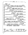
- a timing diagram of the sequencer output is discussed below with reference to the FIG. 3.
- the sequencer 207 is clocked by the clock source whose timing marks 312 are shown in the waveform 311 in FIG. 3.
- the current source amplifier 217 is connected in sequence to the capacitors 219 in response to the counter 239 (keyed to the sampling rate by lead 209) which steps the through connections provided by the multiplexer 218. Since the varactors are essentially non-linear, the non-linear characteristic is compensated by controlling the current output of the current source amplifier as a function of the voltage on the varactor diode. Diode compensation is provided by the amplifier 233.
- a step size control circuit 235 including amplifiers 236 and 237, controls the size of adjustment steps to the capacitors 219 as a function of reductions in peak power. It operates by controlling the time that the current source amplifier delivers current.
- the amplifier 236 generates a triangular wave output and the amplifier 237 operates as a comparator.
- the triangular wave voltage amplifier 237 produces a pulse output which switches the current source amplifier on and off to control the average current output charging the capacitors 219. If the peak power level is high the current source is on most of the time. If the peak power level is relatively low the output current is low and only small adjustments are made to the capacitor voltage levels of capacitors 219.
- the operation of the control circuit may be ascertained by examination of the timing waveforms of FIG. 3.
- the pulses of these waveforms are generated by the sequencer 207. Sequencers are well known in the art and it is not believed necessary to describe its circuitry herein.
- the Pulse 321 of waveform 301 closes switch 211 for the duration of the pulse.
- Pulses 322-325 of waveforms 302-305 subsequently open switch 229 for a period of adjustment whose time interval is determined by the condition of the step size control 235.
- the throughput of the multiplexer 218 is inhibited and switch 229 is closed by a positive voltage on lead 241.
- Pulse 327 of waveform 307 closes switch 212 for the duration of the pulse to provide a sample of the peak power to the comparator 214.
- Pulse 328 of waveform 308 the output of comparator 213 is coupled by the switch 214 to flip flop 216. The sequence is repeated by the application of the pulse 321 of waveform 301 to close switch 211.
- FIG. 4 An alternative arrangement for preventing high to peak-to-average power ratios from occurring is shown in the FIG. 4.
- the system components are identical to those described with reference to the FIG. 1 system, but their relative positioning is altered.
- the chief alteration is the positioning of the voltage controlled phase shifters 431-434 to phase shift the carrier at the outputs of the transceivers 401-404. This repositioning requires phase shifts in the order of 30 to 60 degrees to be effective. Otherwise the operation is substantially similar to the operation of the phase shift system of FIG. 1.
- the control circuit 461 used is identical to the control circuit 161 of FIG. 1 and disclosed in FIG.2 except for the phase shift increment used.
Landscapes
- Engineering & Computer Science (AREA)
- Power Engineering (AREA)
- Amplifiers (AREA)
- Transmitters (AREA)
- Control Of Amplification And Gain Control (AREA)
- Tone Control, Compression And Expansion, Limiting Amplitude (AREA)
Claims (9)
- Verstärkersystem, bei dem mehrere Signale unterschiedlicher Frequenz auf unterschiedlichen Signalkanälen (123 - 126) von einem Leistungskombinator (106) zu einem einzelnen Kanal kombiniert werden, um in einem einzelnen Leistungsverstärker verstärkt zu werden; wobei das Verstärkersystem folgendes enthält:gekennzeichnet durch:eine Vorrichtung zum Minimieren einer Spitzenleistungs-Mischhüllkurve der mehreren Signale; mit:einem Spitzenleistungsdetektor (153), der so geschaltet ist, daß er die Spitzenleistungshüllkurve der kombinierten mehreren Signale erfaßt;einem Komparator (231, 232), der so geschaltet ist, daß er den Spitzenleistungsausgang des Spitzenleistungsdetektors mit einem Referenzleistungspegel vergleicht;Schaltungen zum Justieren einer Phase (131 - 134) mindestens eines der mehreren Signale als Reaktion auf den Komparator, mit:mehreren Signalspeicherelementen (219), die jeweils einem der mehreren Signale zugeordnet sind und jeweils gezielt auf ein Ausgangssignal des Komparators reagieren;mehreren Phasenschiebern (131 - 134), die jeweils einzeln in einen Weg eines der mehreren Signale geschaltet sind und auf das diesem Weg von einem der mehreren Signale zugeordnete Signalspeicherelement reagieren.
- Verstärkersystem nach Anspruch 1, das weiterhin Schaltungen (221, 222) enthält zur Verwertung eines zuvor abgetasteten Spitzenleistungspegels als Referenzsignal, wodurch das Komparatorausgangssignal eine Anzeige für die Amplitudenwanderungsrichtung der Spitzenleistungsamplitude darstellt.
- Verstärkersystem nach Anspruch 2, das weiterhin eine Stromquelle (217) enthält, die auf die Amplitudenwanderungsrichtung reagiert, indem sie an die Signalspeicherelemente eine Ladung anlegt.
- Verstärkersystem nach Anspruch 3, das weiterhin Begrenzungsmittel (231, 232) enthält, um einen Bereich eines von der Stromquelle gelieferten Ausgangsstroms zu steuern.
- Verstärkersystem nach Anspruch 4, das weiterhin eine Multiplexschaltung (218) enthält, um die Stromquelle an ausgewählte Signalspeicherelemente anzukoppeln.
- Verstärkersystem nach Anspruch 5,das weiterhin ein Folgesteuerungsmittel (207) zur Erzeugung einer Folge von Impulsen undeine Schalteinrichtung (218) zum Ankoppeln der Folge von Impulsen an die Signalspeicherelemente enthält.
- Verstärkersystem nach Anspruch 6, das weiterhin einen Komplementflipflop (216) enthält, der den Komparator mit der Stromquelle verbindet.
- Verstärkersystem nach Anspruch 7, das weiterhin ein Mittel (236, 237) zum Steuern eines durchschnittlichen Ausgangsstroms der Stromquelle enthält, wobei das Mittel zum Steuern einen Komparator enthält, der so geschaltet ist, daß er einen Spitzenleistungs-Hüllkurvenleistungspegel mit einer erzeugten welligen periodischen Wellenform vergleicht.
- Verstärkersystem nach Anspruch 8, das weiterhin ein Mittel enthält, das auf das Folgesteuerungsmittel reagiert, indem es den Betrieb der Multiplexschaltung in jeder Periode des Betriebs mindestens einmal sperrt.
Applications Claiming Priority (2)
| Application Number | Priority Date | Filing Date | Title |
|---|---|---|---|
| US07/963,784 US5300894A (en) | 1992-10-20 | 1992-10-20 | Circuitry for minimizing peak power in an amplifier carrying a plurality of signals of differing frequencies |
| US963784 | 1992-10-20 |
Publications (3)
| Publication Number | Publication Date |
|---|---|
| EP0594352A2 EP0594352A2 (de) | 1994-04-27 |
| EP0594352A3 EP0594352A3 (en) | 1994-06-22 |
| EP0594352B1 true EP0594352B1 (de) | 1998-03-04 |
Family
ID=25507707
Family Applications (1)
| Application Number | Title | Priority Date | Filing Date |
|---|---|---|---|
| EP93308164A Expired - Lifetime EP0594352B1 (de) | 1992-10-20 | 1993-10-13 | Schaltung zur Minimisierung der Spitzenleistung in einem Verstärker mit einer Vielzahl von Signalen unterschiedlicher Frequenzen |
Country Status (6)
| Country | Link |
|---|---|
| US (1) | US5300894A (de) |
| EP (1) | EP0594352B1 (de) |
| JP (1) | JP2977424B2 (de) |
| DE (1) | DE69317201T2 (de) |
| ES (1) | ES2114008T3 (de) |
| TW (1) | TW308756B (de) |
Families Citing this family (29)
| Publication number | Priority date | Publication date | Assignee | Title |
|---|---|---|---|---|
| US6175630B1 (en) * | 1993-01-07 | 2001-01-16 | Broadband Innovations, Inc. | Method and apparatus for level and phase control of a plurality of RF signals |
| JPH0738437A (ja) * | 1993-07-19 | 1995-02-07 | Sharp Corp | コーデック装置 |
| US5694395A (en) * | 1994-09-30 | 1997-12-02 | Lucent Technologies, Inc. | Method and apparatus for processing multicarrier signals |
| US5790555A (en) * | 1994-12-05 | 1998-08-04 | Ntt Mobile Communications, Network Inc. | Signal multiplexer and multiplexing method |
| US5745846A (en) * | 1995-08-07 | 1998-04-28 | Lucent Technologies, Inc. | Channelized apparatus for equalizing carrier powers of multicarrier signal |
| FR2781100B1 (fr) * | 1998-07-10 | 2000-10-06 | Thomson Csf | Procede d'elaboration d'un signal d'emission et emetteur a cellules d'amplification pour la mise en oeuvre de ce procede |
| US6445747B1 (en) | 1998-07-14 | 2002-09-03 | At&T Corporation | Method and apparatus to reduce peak to average power ratio in multi-carrier modulation |
| JP2000078072A (ja) * | 1998-08-28 | 2000-03-14 | Hitachi Ltd | 送受信装置 |
| JP3492532B2 (ja) * | 1998-08-28 | 2004-02-03 | 松下電器産業株式会社 | 通信装置及びピーク電力抑圧方法 |
| US6166601A (en) * | 1999-01-07 | 2000-12-26 | Wiseband Communications Ltd. | Super-linear multi-carrier power amplifier |
| US6166598A (en) * | 1999-07-22 | 2000-12-26 | Motorola, Inc. | Power amplifying circuit with supply adjust to control adjacent and alternate channel power |
| US6438360B1 (en) | 1999-07-22 | 2002-08-20 | Motorola, Inc. | Amplifier system with load control to produce an amplitude envelope |
| US6349216B1 (en) | 1999-07-22 | 2002-02-19 | Motorola, Inc. | Load envelope following amplifier system |
| US6160449A (en) * | 1999-07-22 | 2000-12-12 | Motorola, Inc. | Power amplifying circuit with load adjust for control of adjacent and alternate channel power |
| US6128350A (en) * | 1999-08-24 | 2000-10-03 | Usa Digital Radio, Inc. | Method and apparatus for reducing peak to average power ratio in digital broadcasting systems |
| US6434135B1 (en) * | 1999-08-31 | 2002-08-13 | Interdigital Technology Corporation | Adaptive RF amplifier prelimiter |
| AT410153B (de) * | 1999-11-03 | 2003-02-25 | Contraves Space Ag | Verfahren zur synchronisation eines lokalen oszillators in einem optischen homodynempfänger |
| US6954505B2 (en) * | 2001-03-29 | 2005-10-11 | Texas Instruments Incorporated | Discrete multitone modulation with reduced peak-to-average ratio using unloaded subchannels |
| AU2002317839A1 (en) | 2001-06-29 | 2003-03-03 | Telefonaktiebolaget L M Ericsson (Publ) | A transmitter control circuit |
| US7054385B2 (en) * | 2001-10-22 | 2006-05-30 | Tropian, Inc. | Reduction of average-to-minimum power ratio in communications signals |
| US20070211829A1 (en) * | 2001-10-22 | 2007-09-13 | Matsushita Electric Industrial Co., Ltd. | Method and apparatus for pulse optimization for non-linear filtering |
| US8331490B2 (en) * | 2001-10-22 | 2012-12-11 | Panasonic Corporation | Methods and apparatus for conditioning communications signals based on detection of high-frequency events in polar domain |
| US7542517B2 (en) | 2004-02-02 | 2009-06-02 | Ibiquity Digital Corporation | Peak-to-average power reduction for FM OFDM transmission |
| FR2903254B1 (fr) | 2006-06-29 | 2011-04-01 | Thales Sa | Procede et systeme permettant la reorganisation sequentielle de signaux |
| JP5228744B2 (ja) * | 2008-09-25 | 2013-07-03 | 富士通株式会社 | 音声信号処理装置及び音声信号処理方法 |
| DE102008052172B4 (de) * | 2008-10-17 | 2014-01-23 | Fraunhofer-Gesellschaft zur Förderung der angewandten Forschung e.V. | Vorrichtung zum Erzeugen eines Korrektursignals |
| US8175566B2 (en) * | 2009-06-04 | 2012-05-08 | Qualcomm, Incorporated | Multiple multi-mode low-noise amplifier receiver with shared degenerative inductors |
| EP2403137A1 (de) * | 2010-04-26 | 2012-01-04 | Astrium Limited | Hybride Netzwerke |
| US11894075B2 (en) | 2020-08-27 | 2024-02-06 | Yangtze Memory Technologies Co. Ltd. | Non-destructive mode cache programming in NAND flash memory devices |
Family Cites Families (9)
| Publication number | Priority date | Publication date | Assignee | Title |
|---|---|---|---|---|
| US4010426A (en) * | 1975-11-12 | 1977-03-01 | The United States Of America As Represented By The Secretary Of The Air Force | Rf power amplifier parallel redundant system |
| US4064464A (en) * | 1976-04-13 | 1977-12-20 | Westinghouse Electric Corporation | Amplitude stabilized power amplifier |
| US4370622A (en) * | 1981-03-23 | 1983-01-25 | Rockwell International Corporation | IMD Limiter |
| US4546313A (en) * | 1983-03-14 | 1985-10-08 | The United States Of America As Represented By The United States Department Of Energy | Peak power ratio generator |
| US5043673A (en) * | 1989-03-31 | 1991-08-27 | Mitsubishi Denki Kabushiki Kaisha | Compensating circuit for a high frequency amplifier |
| US5045799A (en) * | 1989-09-28 | 1991-09-03 | Rockwell International Corporation | Peak to average power ratio reduction in a power amplifier with multiple carrier input |
| JPH03198407A (ja) * | 1989-12-26 | 1991-08-29 | Mitsubishi Electric Corp | 線形増幅器 |
| US5101211A (en) * | 1991-01-10 | 1992-03-31 | Hughes Aircraft Company | Closed loop RF power amplifier output correction circuit |
| JPH05130191A (ja) * | 1991-10-31 | 1993-05-25 | Nippon Motoroola Kk | マルチサブチヤネル信号の位相制御によるピーク/平均値比率低減方法 |
-
1992
- 1992-10-20 US US07/963,784 patent/US5300894A/en not_active Expired - Lifetime
-
1993
- 1993-10-13 EP EP93308164A patent/EP0594352B1/de not_active Expired - Lifetime
- 1993-10-13 DE DE69317201T patent/DE69317201T2/de not_active Expired - Lifetime
- 1993-10-13 ES ES93308164T patent/ES2114008T3/es not_active Expired - Lifetime
- 1993-10-13 TW TW082108488A patent/TW308756B/zh not_active IP Right Cessation
- 1993-10-19 JP JP5283839A patent/JP2977424B2/ja not_active Expired - Fee Related
Also Published As
| Publication number | Publication date |
|---|---|
| TW308756B (de) | 1997-06-21 |
| US5300894A (en) | 1994-04-05 |
| EP0594352A3 (en) | 1994-06-22 |
| JPH06204773A (ja) | 1994-07-22 |
| JP2977424B2 (ja) | 1999-11-15 |
| DE69317201T2 (de) | 1998-06-25 |
| ES2114008T3 (es) | 1998-05-16 |
| DE69317201D1 (de) | 1998-04-09 |
| EP0594352A2 (de) | 1994-04-27 |
Similar Documents
| Publication | Publication Date | Title |
|---|---|---|
| EP0594352B1 (de) | Schaltung zur Minimisierung der Spitzenleistung in einem Verstärker mit einer Vielzahl von Signalen unterschiedlicher Frequenzen | |
| EP0594358B1 (de) | Verfahren und Vorrichtung zur Reduzierung der Spitzenleistung zur mittleren Leistung in einen Multiträger HF-Komunikationssystem | |
| EP0541789B1 (de) | Vorwärtsgeregeltes verstärkernetzwerk mit gewobbeltem pilotton | |
| EP0585421B1 (de) | Modulationsunabhängiges vorwärts geregeltes verstärkernetzwerk mit hohem dynamikbereich | |
| EP1176734B1 (de) | Digitales Leistungsregelungssystem für einen mehrträger Sender | |
| CA2157255C (en) | Feed-forward amplifier with expanded linearity | |
| US7212791B2 (en) | Transmission device and delay time adjustment method thereof | |
| US5710990A (en) | Transmitter which adjusts peak-to-average power of a multicarrier signal by switching between a group of channels and a phase-adjusted group of channels | |
| US5850162A (en) | Linearization of an amplifier employing modified feedforward correction | |
| US6515544B1 (en) | Multi-terminal power combining feed-forward amplifier | |
| WO1992011694A1 (en) | Feed forward distortion minimization circuit | |
| CN1061123A (zh) | 线性发射机训化的方法和装置 | |
| WO1993018581A1 (en) | Rf power amplifier with linearizattion | |
| US6133791A (en) | Feedforward amplifier with improved characteristics without using pilot signal | |
| US6662018B1 (en) | Analog power control system for a multi-carrier transmitter | |
| JP2001177423A (ja) | Tdma方式デジタル無線送信装置 | |
| US6326840B1 (en) | Feed-forward distortion compensation amplifier and method of amplifying signal with feed-forward distortion compensation | |
| US6949976B2 (en) | Distortion compensating amplifier device, amplifier system, and wireless base station | |
| JPWO2004034574A1 (ja) | 歪み補償増幅装置、増幅システムおよび無線基地局 | |
| AU9258198A (en) | A set-up method for a linearising circuit | |
| JPH0511865B2 (de) | ||
| JP2004193663A (ja) | 歪補償増幅装置 |
Legal Events
| Date | Code | Title | Description |
|---|---|---|---|
| PUAI | Public reference made under article 153(3) epc to a published international application that has entered the european phase |
Free format text: ORIGINAL CODE: 0009012 |
|
| AK | Designated contracting states |
Kind code of ref document: A2 Designated state(s): DE ES FR GB IT NL |
|
| PUAL | Search report despatched |
Free format text: ORIGINAL CODE: 0009013 |
|
| AK | Designated contracting states |
Kind code of ref document: A3 Designated state(s): DE ES FR GB IT NL |
|
| RAP3 | Party data changed (applicant data changed or rights of an application transferred) |
Owner name: AT&T CORP. |
|
| 17P | Request for examination filed |
Effective date: 19941208 |
|
| GRAG | Despatch of communication of intention to grant |
Free format text: ORIGINAL CODE: EPIDOS AGRA |
|
| GRAG | Despatch of communication of intention to grant |
Free format text: ORIGINAL CODE: EPIDOS AGRA |
|
| GRAG | Despatch of communication of intention to grant |
Free format text: ORIGINAL CODE: EPIDOS AGRA |
|
| GRAH | Despatch of communication of intention to grant a patent |
Free format text: ORIGINAL CODE: EPIDOS IGRA |
|
| 17Q | First examination report despatched |
Effective date: 19970701 |
|
| GRAH | Despatch of communication of intention to grant a patent |
Free format text: ORIGINAL CODE: EPIDOS IGRA |
|
| GRAA | (expected) grant |
Free format text: ORIGINAL CODE: 0009210 |
|
| AK | Designated contracting states |
Kind code of ref document: B1 Designated state(s): DE ES FR GB IT NL |
|
| ITF | It: translation for a ep patent filed | ||
| ET | Fr: translation filed | ||
| REF | Corresponds to: |
Ref document number: 69317201 Country of ref document: DE Date of ref document: 19980409 |
|
| REG | Reference to a national code |
Ref country code: ES Ref legal event code: FG2A Ref document number: 2114008 Country of ref document: ES Kind code of ref document: T3 |
|
| PLBE | No opposition filed within time limit |
Free format text: ORIGINAL CODE: 0009261 |
|
| 26N | No opposition filed | ||
| REG | Reference to a national code |
Ref country code: GB Ref legal event code: IF02 |
|
| PGFP | Annual fee paid to national office [announced via postgrant information from national office to epo] |
Ref country code: ES Payment date: 20091023 Year of fee payment: 17 Ref country code: DE Payment date: 20091026 Year of fee payment: 17 |
|
| PGFP | Annual fee paid to national office [announced via postgrant information from national office to epo] |
Ref country code: NL Payment date: 20091016 Year of fee payment: 17 |
|
| PGFP | Annual fee paid to national office [announced via postgrant information from national office to epo] |
Ref country code: IT Payment date: 20091028 Year of fee payment: 17 Ref country code: GB Payment date: 20091022 Year of fee payment: 17 Ref country code: FR Payment date: 20091110 Year of fee payment: 17 |
|
| REG | Reference to a national code |
Ref country code: NL Ref legal event code: V1 Effective date: 20110501 |
|
| GBPC | Gb: european patent ceased through non-payment of renewal fee |
Effective date: 20101013 |
|
| PG25 | Lapsed in a contracting state [announced via postgrant information from national office to epo] |
Ref country code: FR Free format text: LAPSE BECAUSE OF NON-PAYMENT OF DUE FEES Effective date: 20101102 |
|
| REG | Reference to a national code |
Ref country code: FR Ref legal event code: ST Effective date: 20110630 |
|
| PG25 | Lapsed in a contracting state [announced via postgrant information from national office to epo] |
Ref country code: GB Free format text: LAPSE BECAUSE OF NON-PAYMENT OF DUE FEES Effective date: 20101013 Ref country code: NL Free format text: LAPSE BECAUSE OF NON-PAYMENT OF DUE FEES Effective date: 20110501 |
|
| REG | Reference to a national code |
Ref country code: DE Ref legal event code: R119 Ref document number: 69317201 Country of ref document: DE Effective date: 20110502 |
|
| REG | Reference to a national code |
Ref country code: ES Ref legal event code: FD2A Effective date: 20111118 |
|
| PG25 | Lapsed in a contracting state [announced via postgrant information from national office to epo] |
Ref country code: IT Free format text: LAPSE BECAUSE OF NON-PAYMENT OF DUE FEES Effective date: 20101013 |
|
| PG25 | Lapsed in a contracting state [announced via postgrant information from national office to epo] |
Ref country code: ES Free format text: LAPSE BECAUSE OF NON-PAYMENT OF DUE FEES Effective date: 20101014 |
|
| PG25 | Lapsed in a contracting state [announced via postgrant information from national office to epo] |
Ref country code: DE Free format text: LAPSE BECAUSE OF NON-PAYMENT OF DUE FEES Effective date: 20110502 |