EP0594286B1 - Electronic parts with metal wiring and manufacturing method thereof - Google Patents
Electronic parts with metal wiring and manufacturing method thereof Download PDFInfo
- Publication number
- EP0594286B1 EP0594286B1 EP93306663A EP93306663A EP0594286B1 EP 0594286 B1 EP0594286 B1 EP 0594286B1 EP 93306663 A EP93306663 A EP 93306663A EP 93306663 A EP93306663 A EP 93306663A EP 0594286 B1 EP0594286 B1 EP 0594286B1
- Authority
- EP
- European Patent Office
- Prior art keywords
- film
- thin film
- amorphous
- metal wiring
- alloy
- Prior art date
- Legal status (The legal status is an assumption and is not a legal conclusion. Google has not performed a legal analysis and makes no representation as to the accuracy of the status listed.)
- Expired - Lifetime
Links
Images





Classifications
-
- H—ELECTRICITY
- H10—SEMICONDUCTOR DEVICES; ELECTRIC SOLID-STATE DEVICES NOT OTHERWISE PROVIDED FOR
- H10W—GENERIC PACKAGES, INTERCONNECTIONS, CONNECTORS OR OTHER CONSTRUCTIONAL DETAILS OF DEVICES COVERED BY CLASS H10
- H10W20/00—Interconnections in chips, wafers or substrates
- H10W20/40—Interconnections external to wafers or substrates, e.g. back-end-of-line [BEOL] metallisations or vias connecting to gate electrodes
- H10W20/41—Interconnections external to wafers or substrates, e.g. back-end-of-line [BEOL] metallisations or vias connecting to gate electrodes characterised by their conductive parts
- H10W20/44—Conductive materials thereof
- H10W20/4403—Conductive materials thereof based on metals, e.g. alloys, metal silicides
-
- H—ELECTRICITY
- H10—SEMICONDUCTOR DEVICES; ELECTRIC SOLID-STATE DEVICES NOT OTHERWISE PROVIDED FOR
- H10W—GENERIC PACKAGES, INTERCONNECTIONS, CONNECTORS OR OTHER CONSTRUCTIONAL DETAILS OF DEVICES COVERED BY CLASS H10
- H10W20/00—Interconnections in chips, wafers or substrates
- H10W20/40—Interconnections external to wafers or substrates, e.g. back-end-of-line [BEOL] metallisations or vias connecting to gate electrodes
- H10W20/41—Interconnections external to wafers or substrates, e.g. back-end-of-line [BEOL] metallisations or vias connecting to gate electrodes characterised by their conductive parts
- H10W20/435—Cross-sectional shapes or dispositions of interconnections
-
- H—ELECTRICITY
- H10—SEMICONDUCTOR DEVICES; ELECTRIC SOLID-STATE DEVICES NOT OTHERWISE PROVIDED FOR
- H10P—GENERIC PROCESSES OR APPARATUS FOR THE MANUFACTURE OR TREATMENT OF DEVICES COVERED BY CLASS H10
- H10P14/00—Formation of materials, e.g. in the shape of layers or pillars
- H10P14/40—Formation of materials, e.g. in the shape of layers or pillars of conductive or resistive materials
- H10P14/412—Deposition of metallic or metal-silicide materials
-
- H—ELECTRICITY
- H10—SEMICONDUCTOR DEVICES; ELECTRIC SOLID-STATE DEVICES NOT OTHERWISE PROVIDED FOR
- H10W—GENERIC PACKAGES, INTERCONNECTIONS, CONNECTORS OR OTHER CONSTRUCTIONAL DETAILS OF DEVICES COVERED BY CLASS H10
- H10W20/00—Interconnections in chips, wafers or substrates
- H10W20/40—Interconnections external to wafers or substrates, e.g. back-end-of-line [BEOL] metallisations or vias connecting to gate electrodes
- H10W20/45—Interconnections external to wafers or substrates, e.g. back-end-of-line [BEOL] metallisations or vias connecting to gate electrodes characterised by their insulating parts
- H10W20/48—Insulating materials thereof
Definitions
- the present invention relates to electronic parts such as integrated circuit (IC) devices, and particularly to electronic parts with metal wiring having higher reliability e.g., the improved electromigration endurance, and manufacturing method thereof.
- IC integrated circuit
- metal wiring is formed on the surface of an amorphous thin film generally represented by a SiO 2 interlayer insulative film with or without a barrier layer.
- a metal thin film with the high crystalline properties cannot be formed by a so-called epitaxial crystal growth method where a single-crystal thin film can be grown by continuing the crystalline arrangement of an underlayer.
- metal wiring with the excellent electromigration endurance and high reliability is hardly obtained.
- An object of the invention is to provide electronic parts allowing finer elements, higher integration, higher current density, and higher temperature of operation conditions.
- Another object of the invention is to provide electronic parts with highly reliable metal wiring obtained by the formation of a metal thin film with the high crystalline properties.
- a further object of the invention is to provide electronic parts with highly reliable metal wiring obtained by an underlying layer of which electrical resistance in a contact part is satisfactorily low and which can be easily processed, and a metal thin film with the high crystalline properties formed on the underlying layer.
- a still further object of the invention is to provide electronic parts with highly reliable metal wiring simultaneously preventing wiring failures and shortcircuit.
- a still further object of the invention is to provide electronic parts with metal wiring with the improved electromigration and stress-migration endurance.
- a big problem for obtaining a metal thin film with the high crystalline properties is that many crystal nucleuses, from which growth of thin films will start, are simultaneously formed on an underlying layer to be deposited thereon at an initial stage of the deposition. At a film-growing stage, crystal growth of these crystal nucleuses is advanced by absorbing deposited particles or uniting with other nucleuses. However, the size of the crystal nucleuses growing by this mechanism is limited.
- a finally obtained thin film is of polycrystalline where individual crystal grains have different orientation arrangements. Accordingly, in order to form a thin film with the high crystalline properties in a large region, it is important to suppress occurrence of nucleuses as low as possible.
- the interfacial energy ⁇ i depends on 1) lattice matching of a deposited material and underlying material, and 2) interatomic bonding energy between a deposited material and underlying material, in crystal-crystal interface.
- an amorphous material is used as an underlying material like at the time of forming metal wiring in semiconductor devices, it has not been found on what the surface energy of underlying material and interfacial energy depends.
- the inventors have eagerly investigated and examined relationships of atomic arrangement at an interface in detail. As a result, it was found that atomic or molecular arrangement at an interface significantly effected crystal arrangement of a deposited material in the case where an amorphous material is used as an underlying layer as well. Namely, diffraction by X-ray, electron beam and the like revealed that even in an amorphous material, the structure thereof is not completely disordered and there exists regular structure in a small range. As described above, the magnitude of interfaceial energy, which determines atomic arrangement at an interface, is determined by the degree of lattice matching of 2 to 3 periods.
- This small lattice size is substantially the same as an interatomic distance corresponding to a peak of halo pattern which appears in diffraction measurement of an amorphous material.
- this interatomic distance was matched with the spacing of atoms or molecules of a deposited material so that interface energy could be reduced, resulting in the formation of a thin film with the very high crystalline properties.
- the present invention provides an electronic device comprising: an amorphous thin film formed on a substrate, said amorphous thin film having ordered structure over a short range, and a metal wiring having crystalline structure formed directly on the surface of the amorphous thin film; wherein the interatomic distance of the ordered structure of the amorphous thin film approximately matches the spacing of those crystal planes of the metal wiring which include atoms separated by the first-nearest interatomic distance.
- the interatomic distance ds of the amorphous thin film matches with the spacing df of the metal wiring.
- the above particular crystal plane defined with the first-nearest interatomic distance of the metal wiring is, for example, (111), (200) or (220) in fcc structure; (110) in bcc structure; or (002) or (110) in hexagonal system.
- the particular crystal plane is not limited to an orientated plane. Composition of the amorphous thin film varies the degree of match. If the amorphous thin film contains an element mainly constituting the metal wiring, a better matching can be obtained.
- the amorphous thin film preferably contains an element M of which the metal wiring is mainly made. Otherwise, the amorphous thin film preferably contains an element A forming an intermetallic compound with the element M, or an element B capable of continuous series of solid solution with the element M or having the range allowing a complete solid solution.
- Al, Cu, Au, Ag, or W can be generally used as an element M.
- the surface energy of a material in a crystal state constituting the amorphous thin film is preferably larger than the surface energy of a material constituting metal wiring (deposited material).
- the melting point, roughly proportional to the surface energy, of a material in a crystal state constituting the amorphous thin film is desirably high.
- the surface energy of an amorphous material formed of a plurality of elements is defined as the sum of the fractional surface energies of individual elements.
- Substrates of the invention are not particularly limited.
- Conventional semiconductor substrates such as a Si substrate and GaAs substrate, and glass substrates with and without ITO may be used.
- the shape thereof may be flat or have grooves.
- simple metals, alloys or conductive compounds capable of being amorphous are used for an amorphous thin film formed on a substrate. Further, they preferably have composition containing at least one of the above-mentioned elements M, A, and B. Considering the ability of forming amorphous, transition metals, metalloids, semiconductor alloys, and semiconductor compounds are preferable.
- a metal element M III A group elements (Sc, Y, Lanthanide), IV A group elements (Ti, Zr, Hf), V A group elements (V, Nb, Ta), VI A group elements (Cr, Mo, W), VIII group elements (Fe, Ru, Os, Co, Rh, Ir, Ni, Pd, Pt), B, C, N, O, P, Si, and Ge.
- Compounds with perovskite type oxide compositions can be used as an amorphous thin film.
- Amorphous thin films used in this invention are an amorphous thin film where a broad diffraction intensity, namely halo peak, can be measured in diffraction measurements represented by electron diffraction such as RHEED and X-ray diffraction. Diffraction lines from fine crystals such as intermetallic compounds due to incomplete amorphous state are allowed for amorphous thin films used in this invention. Further amorphous thin films used in this invention are not required to be entirely amorphous. Crystalline thin films of which only the surface is amorphous may be used.
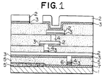
- this amorphous thin film 3 can be used not only as an underlying layer for a single-layer wiring but also as an underlying layer for each metal wiring 2 constituting multi-layer wirings.
- the film 3 can be used as an under-layer for a conductive connecting part in the longitudinal direction such as a via 4 or through hole.
- the film 3 may be formed directly on the substrate 1; or on an interposed layer, for example, an insulative layer 5 such as a SiO 2 thermal oxide film, a barrier layer 6 of Ti, TiN or the like, a contact layer or another wiring above the substrate 1.
- the interposed layer may be flat or have grooves.
- reference numeral 5 indicates an insulative film such as SiO 2 destined for an element isolation area
- reference numeral 7 indicates a doped layer.
- an amorphous thin film between a substrate and metal wiring can suppress reactions caused by grain boundary diffusion in conventional technique.
- an Al amorphous alloy as an amorphous thin film does not form a high resistance reactive layer with metal wiring mainly formed of Al, resulting in a high reliable contact part.
- an alloy containing one of Ta, Nb, V, Mo and W is used as an Al amorphous alloy, a simultaneous fine wiring process for metal mainly formed of Al is possible, thereby reducing the number of processes as compared with the other amorphous alloys.
- the content of Al is preferably 15 at% or more for stabilizing amorphous state.
- the content is more preferably 15 to 80 at% to maintain the surface energy of the amorphous thin film to be high.
- Al amorphous alloys are Td x Al 1-x (0.20 ⁇ x ⁇ 0.85), Nb x Al 1-x (0.20 ⁇ x ⁇ 0.85), V x Al 1-x (0.20 ⁇ x ⁇ 0.60), W x Al 1-x (0.15 ⁇ x ⁇ 0.50) and Mo x Al 1-x (0.25 ⁇ x ⁇ 0.80).
- Cu amorphous alloys have excellent contact properties with metal wiring mainly made of Cu, a contact part with the high reliability can be provided.
- Cu amorphous alloys examples include Ti x Cu 1-x (0.18 ⁇ x ⁇ 0.70), Zr x Cu 1-x (0.18 ⁇ x ⁇ 0.70), Hf x Cu 1-x (0.20 ⁇ x ⁇ 0.70), Y x Cu 1-x (0.10 ⁇ x ⁇ 0.53) and Ta x Cu 1-x (0.20 ⁇ x ⁇ 0.80).
- amorphous alloys such as V x Co 1-x (0.15 ⁇ x ⁇ 0.80), Nb x Cr 1-x (0.25 ⁇ x ⁇ 0.45), Nb x Co 1-x (0.22 ⁇ x ⁇ 0.55), Ta x Cr 1-x (0.25 ⁇ x ⁇ 0.40), Ta x Co 1-x (0.25 ⁇ x ⁇ 0.45), Cr x Co 1-x (0.50 ⁇ x ⁇ 0.70), Mo x Co 1-x (0.20 ⁇ x ⁇ 0.60), and W x Co 100-x (0.20 ⁇ x ⁇ 0.60) are also preferably used since they do not form solid solution, and can avoid the inherent electrical resistance increase by interfacial reaction at elevated temperature for sintering.
- an amorphous thin film may be of multi-layer structure where different amorphous materials are laminated.
- the upper most surface is preferably formed of the above-mentioned amorphous alloys with the high surface energy; and SiO 2 , polyimide, TEOS, SiN and the like containing B or P may be used as the underlying layer of the above multi-layer structure.
- the above-mentioned metal wiring which is formed on an amorphous thin film, is formed of crystal with the high orientation and crystalline properties which is oriented in a given plane direction.
- the angle formed between the normal line direction of the close-packed plane of each crystal grain and the normal line direction of the bottom surface of metal wiring is preferably 80° or less.
- the angle between the close-packed plane and the wiring longitudinal direction is preferably 20° or less.
- metal wiring is formed such that a (111) plane of the close-packed plane in the case where metal wiring crystal structure is fcc structure; a (110) plane in the case of bcc structure; or a (0001) plane in the case of hexagonal structure is approximately parallel to the wiring longitudinal direction.
- the close-packed plane is preferably an upper plane, that is, metal wiring oriented in the close-packed plane is preferably formed.
- This metal wiring can be used not only in a single-layer wiring but also in multi-layer wirings and a conductive connecting part in the longitudinal direction thereof, namely, a via or through hole. Even if a material of the conductive connecting part in the longitudinal direction is different from that of a wiring layer above or under the part, continuity of the crystalline orientation of the metal wiring can be maintained, thus allowing the improved reliability. Further, this metal wiring may be of multi-layer structure where different kinds of metals or metals with different crystal states are laminated.
- Illustrative materials for such metal wirings have the low electric resistance, and are fcc structured pure Al, pure Cu, pure Au, pure Ag, Al-Cu, Al-Ti, Al-Cr, Al-Ta, Al-Mg, Al-In, Al-Li, Cu-Be, Cu-Ag, Au-Pt, Au-Ag, Au-Pd, Au-Cu, bcc structured pure W.
- the amount of addition of a solute is desirably in the range allowing a complete solid solution.
- Si may be contained in 1wt% or less.
- Metals with a high melting point or silicides, nitrides, oxides or carbides of metals with a high melting point may coat on the metal wiring.
- Electronic parts thus constructed of the invention are manufactured in the following manner. First, if necessary, an insulative layer, a barrier layer, a contact layer and the like are formed on a substrate. Thereafter, an amorphous thin film is formed by conventional deposition methods such as a sputter method such that an interatomic distance corresponding to a peak featuring in the diffraction pattern of the amorphous thin film is approximately matched to a particular set of crystal planes of the metal wiring to be formed thereon. Subsequently, while keeping vacuum, the metal wiring is formed If the amorphous thin film is exposed to the air, the surface is cleaned by Ar bias sputtering and the like, and then the metal wiring is formed.
- a sputter method such that an interatomic distance corresponding to a peak featuring in the diffraction pattern of the amorphous thin film is approximately matched to a particular set of crystal planes of the metal wiring to be formed thereon.
- metal wiring may be formed without surface cleaning.
- desirable methods for forming a metal thin film by physical vapor deposition include a sputter method, bias sputter method and ion beam method.
- Desirable methods for forming a metal thin film by chemical vapor deposition include, for example in the case of an Al-CVD method, a thermal chemical vapor deposition (CVD) method with the use of alkylaluminum such as TIBA or alkylaluminum hydride such as DMAH as a source gas.
- CVD thermal chemical vapor deposition
- Si or Cu may be contained in the source gas during film deposition.
- An alloy may be made by lamination by ion implantation or sputtering, and subsequent heat treatment after film deposition.
- an amorphous thin film and metal wiring may be formed thereon via an insulative layer and the like to construct multi-layer wirings.
- a graphoepitaxy method may be used with processing the surface of the substrate. It is previously described that crystal of a metal thin film formed on an amorphous thin film of an underlying layer with the high surface energy has the extremely high orientation, and is oriented in a given plane direction. It appears that if the surface energy of the under layer is high, a wetting angle of nucleuses vapor-deposited is small and thereby, for example in the case of Al, a (111) plane with low surface energy can stably grow. However, at this time, directions in a plane of the growing nucleuses are at random. Thus, control of directions in a plane is required for the higher wiring reliability.
- an amorphous thin film with grooves formed thereon is used as an underlying layer, and thereby not only the crystalline properties of a metal thin film to be formed but also control of directions in a plane are sufficiently enhanced.
- the bottom part of the grooves may be made of a material different from or identical to that of which the side wall part is made.
- the bottom part and side wall part of the grooves are made of different materials and difference therebetween in the surface energy is utilized at the time of forming a metal thin film. The reasons therefor are as follows; A material to be deposited orientates and grows in a part with higher surface energy than the bottom or side wall part with lower surface energy.
- direction of the other axis of deposited film can be controlled at an interface with the other low-surface-energy part.
- a metal thin film similar to single crystal can be formed.
- a metal thin film with the high crystalline properties can be obtained.
- Desirable grooves are as follows:
- the shape of the grooves is a stripe, rectangle, square, regular triangle or combination thereof. Many of such grooves are arranged such that one side of the groove is parallel to one of the other groove with accuracy of ⁇ 5°.
- the width of each groove is the average grain size of metal wiring or less and the space of each groove is also the average grain size of metal wiring or less. In the case of stripe-like grooves, the groove width and space are preferably the average grain size of metal wiring or less.
- a preferable method for removing a surface oxide of the amorphous thin film is plasma etching immediately before the deposition of a metal thin film. After etching, it is important to maintain the vacuum to be 1 x 10 -6 Torr or less.
- a CVD method or PVD method may be applied as a method for forming a metal thin film.
- a substrate temperature is preferably raised to promote migration of deposited particles by means such as resistance heating, electron beam irradiation and laser beam irradiation. Further, an oblique vapor deposition method, where a vapor deposited particle flux is oblique against a substrate, is preferable.
- Illustrative methods for depositing a conductor layer are various CVD methods as well as physical vapor deposition methods such as a sputtering method and resistance heating vapor deposition method.
- Illustrative materials of which the conductor layer is formed are Si, WSi, MoSi, pure Al, an Al alloy, pure Cu, a Cu alloy, W, Au, and Ag.
- Desirable Al alloys are an Al-Cu alloy, Al-Cr alloy and Al-Mg alloy. Alternatively, these materials may be layer-like laminated.
- film-deposition is preferably performed by a thermal CVD method with the use of alkylaluminum such as TIBA or alkylaluminum hydride such as DMAH as a source gas.
- alkylaluminum such as TIBA
- alkylaluminum hydride such as DMAH
- Si or Cu may be contained in the source gas during film deposition.
- An alloy may be made by lamination by ion implantation or sputtering, and subsequent thermal treatment after film deposition.
- a given thermal treatment may be conducted for the purpose of further crystal grain growth in metal wiring of highly orientated crystal.
- the amorphous thin film is allowed to be crystallized or disappear by the thermal treatment. Since its crystalline property is improved by the crystal grain growth of the highly orientated crystal, the reliability of the metal wiring can be further improved.
- the present invention relates to the improvement in the reliability of metal wiring as mentioned above, the technique of the invention can be similarly applied to an electrode part of a capacitor or resistance heater in an electronic part.
- an under electrode of a capacitor if an interatomic distance corresponding to a peak of halo pattern appearing in diffraction measurement of an amorphous thin film of an underlying layer approximately matches with a spacing of a particular crystal plane defined with the first adjacent interatomic distance of the under electrode, the interface energy between the amorphous thin film and under electrode is reduced so that the under electrode with the very excellent crystalline properties can be formed. Accordingly, the crystalline properties of a dielectric thin film formed thereon is enhanced.
- an amorphous thin film is used as a resistance heater uniform and stable electrical resistance can be attained. Further if an electrode is deposited on this amorphous thin film such that the interatomic distance of the amorphous thin film approximately matches with the spacing of the electrode, the crystalline properties of the electrode are improved and electromigration induced degradation is suppressed at the time of a large current application.
- Fig. 1 is a sectional view showing a layer-structure of the invention.
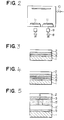
- Fig. 2 is a view showing a multi-target sputter apparatus for use in the invention.
- Fig. 3 is a sectional view according to Example 1.
- Fig. 4 is a sectional view according to Example 3.
- Fig. 5 is a sectional view according to Example 5.
- Fig. 6 is a sectional view according to Example 6.
- Fig. 7 is a sectional view according to Example 7.
- Fig. 8 is a sectional view according to Example 8.
- Figs. 9 (a) to (f) are sectional view showing a method for forming a wiring according to Example 9.
- Fig. 10 is a view showing results of an accelerated test according to Example 9.
- Fig. 11 is a sectional view according to Example 10.
- Fig. 12 is a plan view showing a test substrate with a wiring part according to Example 11.
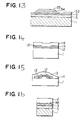
- Fig. 13 is a sectional view according to Example 14.
- Fig. 14 is a sectional view according to Example 16.
- Fig. 15 is a sectional view according to Example 17.
- Fig. 16 is a sectional view according to Example 18.
- Fig. 17 is a sectional view according to Example 19.
- Figs.18 (a) to (g) are sectional views according to Example 21.
- Fig. 19 is a sectional view according to Example 21.
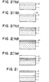
- Figs.20 (a) to (e) are sectional views showing a flow of steps according to Example 23.
- Fig. 21 is a sectional view according to Example 25.
- Fig. 22 is a sectional view according to Example 28 and Example 29.
- Fig. 23 is a view showing a four-terminal pattern according to Example 35.
- an amorphous thin film 3 and metal wiring 2 were successively formed by sputtering.
- an AlTa film was formed as an amorphous thin film 3 by means of a multi-target sputter apparatus as shown in Fig. 2.
- the sputtering conditions are shown below.
- reference numeral 8 indicates a high frequency power source, 9 a matching circuit, 10 a mass flow controller, 11 a target.
- composition analysis revealed that the formed film was Al 40 Ta 60 (hereinafter, numeral value shows ratio of an atomic composition).
- X-ray diffraction revealed that the film was amorphous and that an interatomic distance ds corresponding to peak of halo pattern was 2.34 ⁇ .
- a spacing df of Al (111) was 2.34 ⁇
- the spacing ds can match with the spacing of a particular crystal plane of the metal wiring.
- a mosaic target was used.
- other methods such as simultaneous sputtering with the use of a binary target and lamination of each element could produce a similar amorphous thin film.
- Al was sputtered on the Al 40 Ta 60 film.
- the sputtering conditions are shown below.
- the Al film thus formed was evaluated for the orientation and crystalline properties by X-ray diffraction.
- the full width of half-maximum (hereinafter referred to as FWHM) of a (111) rocking curve (orientation FWHM) was 1.2° and bragg reflection other than (hhh) reflection, for example (200), (220) or the like, was not observed.
- the film thus formed with a layer-structure shown in Fig. 3 was processed into a four-terminal pattern 0.5 ⁇ m in width and 1mm in length, and subjected to an electromigration (EM) test.
- the test conditions were that a wiring temperature was 200°C and a current density was 2x10 6 A/cm 2 .
- EM electromigration
- an amorphous thin film and metal wiring (an amorphous thin film/metal wiring); that is, (Pt 21 Zr 79 /Pt), (Cu 50 Ti 50 /Cu), (Ag 55 Cu 45 /Ag), and (Fe 80 B 20 /Fe); were formed. Similar evaluation of the orientation FWHM revealed that Pt, Cu and Ag were (111) orientation and the FWHMs thereof were 1.4°, 1.8° and 1.6° respectively; and Fe was (110) orientation and the orientation FWHM of (110) reflection thereof was 1.7°.
- Example 1 an amorphous thin film made of Ni 30 Ta 70 (melting point of intermetallic compound of Ni 30 Ta 70 : 1500°C) was formed and a metal wiring made of Al (melting point: 660°C) was formed thereon.
- the amorphous thin film contained an element which has a melting point higher than that of a metal wiring and which could constitute an intermetallic compound with a main element forming the metal wiring.
- an interatomic distance ds of Ni 30 Ta 70 corresponding to a peak of halo pattern was 2.33 ⁇ . This approximately matches with a spacing df 2.34 ⁇ of Al (111).
- (111) orientation FWHM of 0.9° and excellent crystalline properties were observed. Further, in the EM test, it was confirmed that even after an elapsed time of 1000 hours there was no failure and excellent reliability was also obtained.
- an amorphous thin film and metal wiring that is, (Pd 80 Si 20 /Al), (Ag 55 Cu 45 /Al), and (W 70 Zr 30 /Al); were formed. Similar evaluation revealed that the (111) orientation FWHMs thereof were 1.9°, 1.8° and 1.2 respectively.
- Example 1 an amorphous thin film made of a Co-based alloy, Co 80 Zr 9 Nb 11 was formed and a metal wiring made of Al was formed thereon.
- an interatomic distance ds of Co 80 Zr 9 Nb 11 corresponding to a peak of halo pattern was 2.04 ⁇ . This approximately matches with a spacing df 2.02 ⁇ of Al (200).
- (111) orientation and excellent crystalline properties were observed. Further, in the EM test, it was confirmed that even after an elapsed time of 1000 hours there was no failure and excellent reliability was obtained.
- an amorphous thin film and metal wiring (an amorphous thin film/metal wiring); that is, (Co 80 Zr 8 Nb 12 /Al), (Co 85 Zr 6 Nb 9 /Al), (Co 88 Zr 8 Ta 9 /Al), and (Co 90 Hf 6 Pd 4 /Al); were formed. Similar evaluation revealed that the (111) orientation FWHMs thereof were 1.2° and satisfactory crystalline properties was obtained.
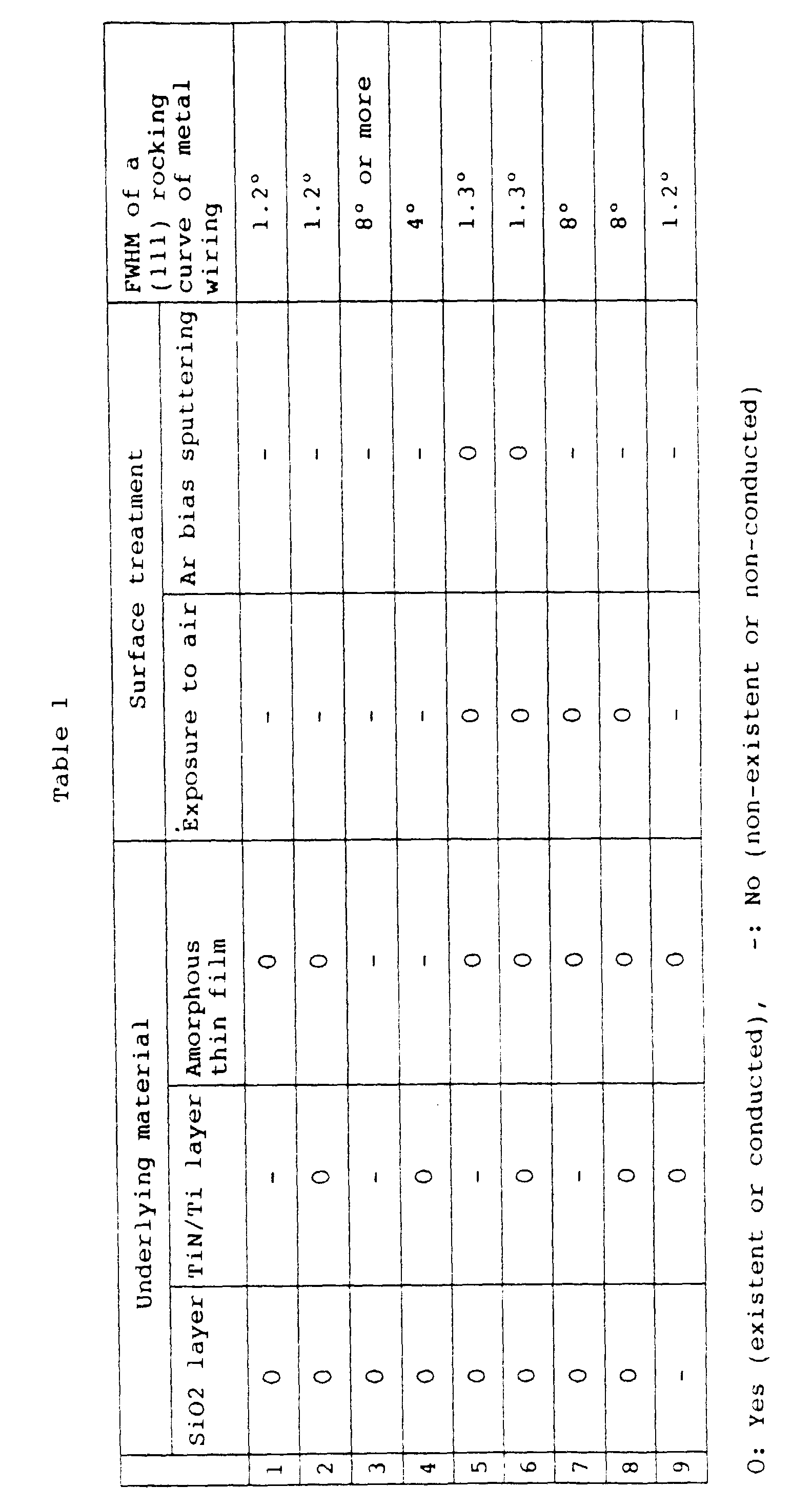
- Al metal wirings 2 were formed after various combinations of the following steps; these steps were that a polycrystalline TiN/Ti layer was formed on the insulative layer 5 as a barrier layer 6, that an amorphous thin film 3 (Co 80 Zr 9 Nb 11 ) was formed thereon, that thereafter it was exposed to the air as shown in Table 1, and that it was then subjected to Ar bias sputtering.
- the crystalline orientation of these Al metal wirings were evaluated with the FWHM of an Al(111) rocking curve by X-ray diffraction using a CuK ⁇ line. As shown in Table 1, in the cases of no amorphous thin film and no Ar bias sputtering after exposure to the air, the crystalline orientation was remarkably degraded.
- Example 2 amorphous thin films and metal wirings shown in Table 2 were formed. As also shown in Table 2, in this embodiment, amorphous thin films with larger surface energy than that of metal wiring in the crystalline state were used.
- borides, carbides and nitrides of TiB 2 and the like were preferably used as an amorphous thin film, since their surface energy was large.
- a metal wiring was directly formed on SiO 2 in a similar way to Example 1.
- An interatomic distance ds of SiO 2 corresponding to a peak of halo pattern does not approximately match even for the nearest spacing df of (111) Al. Further, the surface energy of SiO 2 is smaller than that of Al.
- the (111) orientation FWHM was as large as 8.2° and in the EM test a wiring failure was observed within 10 hours.
- a conductive connecting part 4 namely a via
- a SiO 2 thermal oxide film was formed as an insulative layer 5 on a Si substrate 1 and thereafter a 4000 ⁇ thick thin film, which was made of Al, Cu, W or MoSi 2 , was deposited as a under-layer metal wiring 2'.
- a 3000 ⁇ thick SiO 2 interlayer insulative film 5' was deposited by means of a thermal CVD method.
- a via (or through hole) 4 with a diameter of 50 ⁇ m was formed by means of conventional PEP, reactive ion etching (RIE) steps.
- RIE reactive ion etching
- the via 4 was filled with W by a selective CVD method.
- a 200 ⁇ thick Co 80 Zr 9 Nb 11 thin film was formed as an amorphous thin film 3 of the present invention.
- the surface of Co 80 Zr 9 Nb 11 was exposed to the air one time, it was subjected to Ar RF plasma cleaning.
- pure Al thin film was deposited as a metal wiring 2 in a thickness of 4000 ⁇ by sputtering.
- the crystalline orientation of the Al thin film was evaluated with the FWHM of an Al (111) rocking curve by X-ray diffraction using a CuK ⁇ line.
- Example 5 a via 4 was formed and then, as shown in Fig. 7 , Al 40 Ta 60 was formed as an amorphous thin film 3 by sputtering.
- provision of a collimator between a substrate with the via and target improved the direct-advance property of particles to be deposited. Accordingly, an amorphous layer was hardly formed on a side wall of the via 4 and a 100 ⁇ Al-Ta amorphous thin film 3 could be formed on the bottom surface of the via 4 and interlayer insulative film 5'.
- Ar RF bias sputter cleaning After exposure to the air one time, it was subjected to Ar RF bias sputter cleaning. Then pure Al thin film was deposited in a thickness of 4000 ⁇ as a metal wiring 2 by sputtering.
- FWHM was uniformly 1.1°.
- an Al 40 Nb 60 film was formed as an amorphous thin film 3' on an insulative layer 5 formed of a SiO 2 thermal oxide film, and thereafter under vacuum of 1 x 10 -7 Torr or less pure Al was continuously deposited to form an under-layer metal wiring 2' with a thickness of 4000 ⁇ .
- the FWHM of a rocking curve of the under-layer metal wiring 2' was 1.2°.
- a SiO 2 interlayer insulative film 5' and via 4 were formed on the Al under-layer metal wiring 2'.
- the via 4 was selectively filled with Al by means of a thermal CVD method using TIBA (triisobuthyl aluminum, i-(C 4 H 9 ) 3 Al) as a source gas.
- TIBA triisobuthyl aluminum, i-(C 4 H 9 ) 3 Al
- This Al with which the via 4 was filled had the continuous crystalline orientation of the lower Al and had the same FWHM of a rocking curve as that of the under-layer metal wiring 2'.
- Al-Nb was continuously deposited in a thickness of 250 ⁇ as an amorphous thin film 3 by sputtering.
- an Al film was deposited in a thickness of 250 ⁇ as a metal wiring 2 by means of a sputter or thermal CVD method using TIBA.
- the distribution of the crystalline orientation of this Al film was uniform and the rocking FWHM was 1.2 °.
- Al may be deposited after removing an amorphous thin film 3 corresponding to the via 4 by a conventional PEP step and ion-milling step. Even the Al film thus obtained had the uniform orientation including the via part, and the FWHM was similarly 1.2 °.
- an insulative layer formed of amorphous SiO 2 was formed on the surface of a Si substrate 1.
- a 1000 ⁇ thick amorphous thin film 3 was deposited on the amorphous SiO 2 by a sputter method (Fig. 9 (b)) and then the amorphous thin film 3 on parts other than parts on which wiring would be formed were removed by etching (Fig. 9 (c)).
- a 5000 ⁇ thick insulative layer 5 formed of amorphous SiO 2 was uniformly deposited thereon (Fig. 9 (d)).
- only SiO 2 on the amorphous thin film 3 was removed by etching to form a groove in which wiring would be arranged (Fig. 9 (e)).
- the bottom surfaces of the grooves were made of the amorphous thin film 3.
- the width of the grooves, the width of the metal wiring was 0.8 ⁇ m and the depth of the grooves was 4000 ⁇ .
- An ion beam with low energy was irradiated on the above substrate 1 with the grooves to remove an oxide film on the surface of the amorphous thin film 3.
- Al was deposited by means of a thermal CVD method using TIBA to obtain a metal wiring 4 (Fig. 9 (f)). Selective growth that Al was deposited only in the grooves could be performed at a substrate temperature of 300°C or lower.
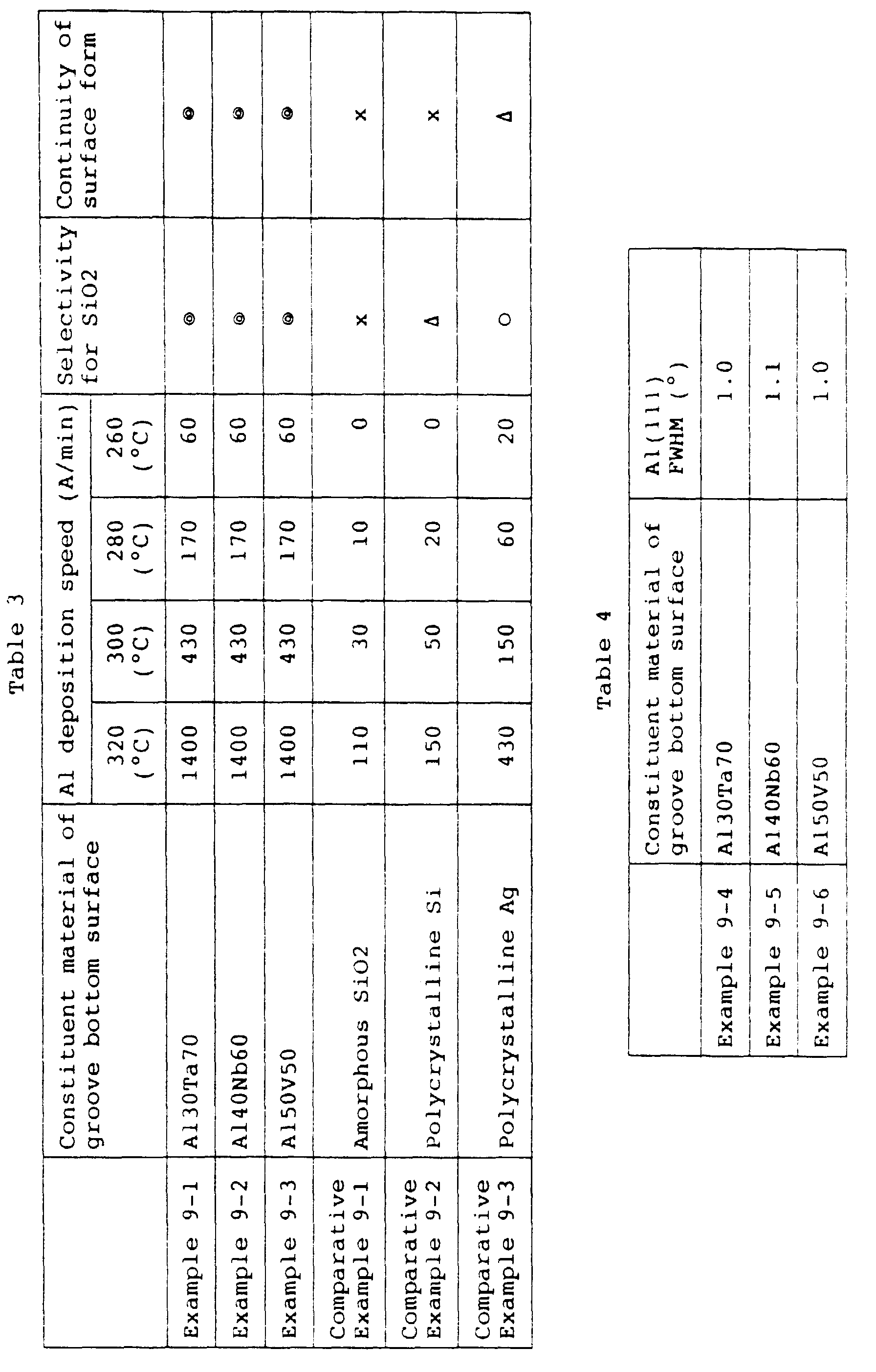
- Table 3 shows the Al deposition speed in the grooves against substrate temperatures in the case where an Al amorphous alloy, as the amorphous thin film 3, was formed on the groove bottom surface.
- the Al amorphous alloys include Al 30 Ta 70 , Al 40 Nb 60 , and Al 50 V 50 . Further, in order to confirm the selective growth, Table 3 also shows if selective growth for SiO 2 was performed in parts other than the grooves. As comparative examples, a film of amorphous SiO 2 , polycrystalline silicon or polycrystalline silver was formed on the groove bottom surface. The Al deposition speeds and selective growth of the comparative examples are shown in Table 3.
- Al filled in the grooves whose bottom was formed of the Al amorphous alloy was examined by a transmission electron microscope.
- the examination revealed that a diameter of Al crystal grains was about 1 ⁇ m to be substantially the same as the wiring width and that these (111) crystal grains were connected with small angle grain boundaries in the line direction of the wiring. Further, there existed a region which consisted of one crystal grain with length of 10 ⁇ m or more in the wiring line direction. This exhibits that a single-crystal Al wiring was partially obtained which had more excellent stress-migration and electromigration endurance than those of (111) high orientation.
- a SiO 2 insulative layer 5 was formed on a semiconductor substrate 1 with a functional element 31 by means of a CVD method.
- a region destined for a contact part was removed by etching to from a contacting hole 32.
- a natural oxide film which was formed on the semiconductor substrate 1 of the contacting hole bottom surface was removed by hydrofluoric acid cleaning.
- it was rinsed with pure water with a low oxygen concentration and then dried by highly pure nitrogen gas purge.
- An Al-Ta amorphous thin film 3 was formed on the substrate by a multi-sputter apparatus. The sputtering conditions are shown below.
- composition analysis revealed that the formed film was Al 55 Ta 45 .
- X-ray diffraction revealed that the film was amorphous.
- the Al amorphous thin film 3 was formed by a sputter method in this embodiment, a similar amorphous film can be formed by a CVD method or vapor deposition method.
- a Al-Ta mosaic target was used in the sputtering of the Al amorphous thin film 3
- a similar amorphous thin film can be obtained by the other methods such as simultaneous sputtering with an Al/Ta binary target or alternate laminating Al and Ta in thin thicknesses.
- an Al film was formed thereon by a sputter method.
- the sputtering conditions are shown below.
- the Al film thus formed was evaluated for the orientation and crystalline properties by X-ray diffraction.
- the FWHM of a (111) rocking curve was 1.0° and excellent orientation was observed. Namely satisfactory orientation was obtained.
- the Al film was formed by a sputter method in this embodiment, similarly satisfactory layers can be obtained by means of a CVD method and vapor deposition method.
- an Al-Ta amorphous thin film and Al film were formed on a silicon substrate with a thermal oxide film under condition similar to Example 10.
- a test substrate 24 was made which had an anode 21, a cathode 22 and a 0.8 ⁇ m wide wiring part 23 connecting these electrodes.
- the orientation and crystalline properties of an Al film of this test substrate was evaluated by X-ray diffraction.
- the FWHM of a (111) rocking curve was 1.0°.
- a current at a current density of 2 x 10 6 A/cm 2 was flown in the test substrate 24 at a test temperature of 200°C to measure its average failure time. The value was 1000 hours or more, thereby exhibiting that the test substrate had the high electromigration endurance.
- Al-Mo amorphous thin film was formed on a substrate with functional elements thereon.
- the formed film was Al 60 Mo 40 .
- X-ray diffraction revealed that the film was amorphous.
- An Al film formed thereon was evaluated for the orientation and crystalline properties by X-ray diffraction. As a result, the FWHM of a (111) rocking curve was 1.1°. Satisfactory orientation was observed.
- Example 10 Al-Nb-Si amorphous thin film was formed on a substrate with functional elements thereon. As a result of composition analysis, it was found the formed film was Al 40 Nb 55 Si 5 . X-ray diffraction revealed that the film was amorphous. An Al film formed thereon was evaluated for the orientation and crystalline properties by X-ray diffraction. As a result, the FWHM of a (111) rocking curve was 1.3°. Excellent orientation was observed.
- a six-inch silicon wafer with a 4000 ⁇ insulative film 5 formed of a thermal oxide film was used as a substrate 1.
- a PtZr amorphous thin film 3 was formed by means of a multi-target sputter apparatus as shown in Fig. 5. The sputtering conditions are shown below.
- composition analysis revealed that the formed film was Pt 21 Zr 79 .
- X-ray diffraction revealed that the film was amorphous.
- the Pt film 33 thus formed as an under electrode was evaluated for the orientation and crystalline properties by X-ray diffraction.
- the (111) orientation FWHM was 1.4° and satisfactory crystalline properties were observed.
- a strontium titanate film 34 was formed as a dielectric thin film by means of a RF magnetron sputter method.
- a sintered body of strontium titanate was used as a target. The sputter conditions are shown below.
- the orientation and crystalline properties of the dielectric thin film were evaluated by X-ray diffraction.
- the (111) orientation of Pt film 33 was continued and the (111) orientation FWHM was 1.5°.
- An Au film 35 was vapor deposited on this dielectric thin film as an upper electrode and the capacitor property thereof was evaluated. It was found that dielectric constant and leak current were satisfactory values.
- the orientation FWHM of a Pt film directly formed on the thermal oxide film was 9.2°. When a strontium titanate film was formed thereon under the above conditions, the orientation FWHM was 9.5°.
- Example 14 using a six-inch silicon wafer substrate with a 4000 ⁇ thermal oxide film, a Pt 21 Zr 79 film was formed as an amorphous thin film by means of a multi-target sputter apparatus.
- a PtTi film was formed by sputtering as an under electrode on the amorphous Pt 21 Zr 79 film.
- the sputter conditions are shown below.
- the PtTi film thus formed was subjected to composition analysis.
- the analysis revealed that the composition thereof was Pt 88 Ti 12 .
- the orientation and crystalline properties thereof were evaluated by X-ray diffraction.
- the (111) orientation FWHM was 1.4° and satisfactory crystalline properties were observed.
- a ferrodielectric thin film of lead titanate zirconate was grown by means of a RF magnetron sputter method.
- a used target was a sintered body where powder of lead titanate zirconate added with lead oxide 10 mol% rich was sintered at 1200°C. The sputtering conditions are shown below.
- the orientation and crystalline properties of the obtained strong dielectric thin film were evaluated by X-ray diffraction.
- the (111) orientation of the PtTi film was continued and the (111) orientation FWHM was 1.9°.
- the orientation FWHM of a Pt film directly formed on the thermal oxide film was 9.2°.
- the orientation FWHM was 9.8°.
- an AlTa amorphous thin film was formed as a resistance heater film 12 by means of a multi-target sputter apparatus as shown in Fig. 2.
- the sputter conditions are shown below.
- the formed film was Al 25 Ta 75 .
- X-ray diffraction revealed that this film was amorphous.
- an Al thin film was sputtered thereon. The sputter conditions are shown below.
- the crystalline properties of the formed film were evaluated by X-ray diffraction. This film was an oriented film with the FWHM 1.0° of a (111) rocking curve.
- an AlNa thin film was formed as a resistance exothermic body film 12 by means of a multi-target sputter apparatus as shown in Fig. 2.
- the sputter conditions are shown below.
- the formed film was Al 40 Nb 60 .
- X-ray diffraction revealed that this film was amorphous.
- This Al-Nb film was processed by lithography and etching steps to remain only on the height and vicinity thereof. Next this was placed in a chamber again and subjected to Ar bias cleaning. Then an Al film was sputtered. The sputter conditions are shown below.
- the crystalline properties of the Al film formed on the flat part were evaluated by X-ray diffraction.
- This film was an oriented film with the FWHM of 1.2° of a (111) rocking curve.
- an AlTa amorphous film 3 was formed by means of a multi-target sputter apparatus as shown in Fig. 2. The sputter conditions are shown below.
- composition analysis revealed that the formed film was Al 45 Ta 55 .
- X-ray diffraction revealed that the film was amorphous.
- grooves 38 were formed by standard lithography and RIE steps.
- the depth of the grooves 38 was 100 ⁇ and the width thereof was 1000 ⁇ .
- AlTa amorphous thin film 3 with the grooves 38 was subjected to Ar bias cleaning, an Al film was sputtered.
- the sputter conditions are shown below.
- the Al film thus formed was evaluated for the orientation and crystalline properties by X-ray diffraction.
- the (111) orientation FWHM was 1.2° and satisfactory crystalline properties were observed.
- a test substrate 24 had an anode 21, a cathode 22 and a 0.8 ⁇ m wide wiring part 23 connecting these electrode.
- the test substrate 24 was made by standard lithography and RIE steps. A current at a current density of 2 x 10 6 A/cm 2 was flown to the wiring part 23 of the test substrate 24 at a test temperature of 200°C. It was confirmed that even after the elapsed time of 1000 hours there was no failure. This exhibits that since Al film was highly oriented and the Al film was a film formed only of small angle grain boundaries, the electromigration endurance was dramatically enhanced.
- grooves were formed by means of standard lithography and RIE steps.
- a NiTa amorphous film 3 with grooves 30 was formed on the substrate 1 by means of a multi-target sputter apparatus as shown in Fig. 2.
- the sputter conditions are shown below.
- composition analysis revealed that the formed film was Ni 50 Ta 50 .
- X-ray diffraction revealed that the film was amorphous.
- a sectional surface was examined by a SEM. The examination revealed that the grooves 30 were uniformly formed in the surface of NiTa amorphous film 3, the depth of the grooves 30 being 1000 ⁇ , the width thereof being 1000 ⁇ .
- Example 18 After the NiTa amorphous thin film 3 was subjected to Ar bias cleaning, Al was sputtered in a manner similar to Example 18. The formed Al film was evaluated for the orientation and crystalline properties by X-ray diffraction. The (111) orientation FWHM was 0.9° and satisfactory crystalline properties were observed.
- an AlNb amorphous thin film was formed by means of a multi-target sputter apparatus as shown in Fig. 2.
- the sputter conditions are shown below.
- composition analysis revealed that the formed film was Al 40 Nb 60 .
- X-ray diffraction revealed that the film was amorphous.
- grooves were formed by standard lithography and RIE steps.
- the depth of the grooves was 100 ⁇ and the width thereof was 1000 ⁇ .
- Al-0.1at%Cu was sputtered as a metal thin film.
- the sputter conditions are shown below.
- the AlCu film thus formed was evaluated for the orientation and crystalline properties by X-ray diffraction.
- the (111) orientation FWHM was 0.9° and satisfactory crystalline properties were observed.
- the orientation was further enhanced and the (111) orientation FWHM become 0.7°.
- a 1000 ⁇ thick thermal oxide film was formed on a Si (100) six-inch substrate 1 as an insulating layer 5. Thereafter, the following seven samples were prepared.
- L/S is shown in Fig. 19.
- polycrystalline Ta surface energy: 2150erg/cm 2
- polycrystalline Ta was sputtered on the thermal oxide film to form a 200 ⁇ thick Ta film 39.
- a 1000 ⁇ thick thermal oxide film was formed on Si(100) six-inch substrates and then a 200 ⁇ thick Ta-40at%Al film was deposited by sputtering. These samples were processed to form grooves of L/S as shown in Table 6 by RIE. The resultant samples were subjected to Ar plasma etching in a high vacuum sputter whose the degree of vacuum was on the order of 10 -10 Torr so that a surface oxide film of the Al-Ta film surface was removed by Ar plasma etching. Subsequently, a pure Al film was formed in a thickness of 4000A. The EM test was conducted in a manner similar to Example 21. The results are shown in Table 6.
- grooves 36 were formed by standard lithography and RIE steps (Fig.20 (b)). The depth of the grooves 36 was 100 ⁇ and the width thereof was 1500 ⁇ .
- a AlTa amorphous film 3 was formed on this substrate 1 by means of a multi-target sputter apparatus as shown in Fig. 2 (Fig. 20 (c)).
- the sputter conditions are shown below.
- composition analysis revealed that the formed film was Al 75 Ta 25 .
- X-ray diffraction revealed that the film was amorphous.
- this substrate 1 was subjected to thermal treatment at 450°C for 30 minutes so that the AlTa amorphous thin film 3 was crystallized to form an intermetallic compound of Al 3 Ta or a polycrystalline film 37 with small angle grain boundaries in a grain diameter of 1 to 2 ⁇ m (Fig. 20 (d)).
- an Al film was sputtered thereon (Fig. 20 (e)). The sputter conditions are shown below.
- the Al film thus formed was evaluated for the orientation and crystalline properties by X-ray diffraction.
- the (111) orientation FWHM was improved to be 0.3° and almost grain boundaries remaining in the Al film were small angle boundaries.
- a test substrate 24 had an anode 21, a cathode 22 and a 0.8 ⁇ m wide wiring part 23 connecting these electrode.
- the test substrate 24 was made by standard lithography and RIE steps. A current at a current density of 2 x 10 6 A/cm 2 was loaded to the wiring part 23 of the test substrate 24 at a test temperature of 200°C. Even after the elapsed time of 1000 hours there was no failure. This exhibits that since the Al film was similar to single-crystal, the electromigration endurance was dramatically enhanced.
- grooves were formed by standard lithography and RIE steps.
- the depth of the grooves was 500 ⁇ and the width thereof was 5000 ⁇ .
- the space between the grooves was 3000 ⁇ .
- a AlNb amorphous film was formed on this substrate by means of a multi-target sputter apparatus as shown in Fig. 5.
- the sputter conditions are shown below.
- composition analysis revealed that the formed film was Al 75 Nb 25 .
- X-ray diffraction revealed that the film was amorphous.
- this substrate was heated at 450°C for 30 minutes so that the AlNb amorphous film was crystallized to form an intermetallic compound of Al 3 Nb.
- the intermetallic compound was filled in the grooves to be of single-crystal.
- the surface of the resultant substrate was flatted by polishing and then was placed into a chamber again. After Ar bias cleaning, an Al-0.1at%Cu alloy was sputtered as a metal thin film. The sputter conditions are shown below.
- the AlCu film thus formed was processed into a metal wiring by a RIE step. Moreover, in the EM test under the same conditions as those of Example 23, even after the elapse of 1000 hours there was no failure.
- a 4000 ⁇ thick pure Al thin film destined for a metal wiring 2 was formed by sputtering.
- an Al-Ta amorphous thin film 3 was formed by sputtering using an Al/Ta mosaic target. The thickness of the layer 3 varied 100, 300, and 500 ⁇ .
- some samples were exposed to the air. The exposed samples were then placed into a sputter apparatus again so that the Al-Ta amorphous thin film 3 was formed on the pure Al thin film.
- a surface oxide of the exposed samples was removed by RF-Ar plasma where the substrate 1 side was an electrode.
- plasma etching was conducted until a clear diffraction pattern of an Al thin film was observed by RHEED for the surface of the Al thin film.
- the composition of the amorphous thin film 3 was Al 20 Ta 80 .
- the laminated structure of the metal film 2 of a pure Al and Al-Ta amorphous thin film 3 was thus prepared.
- these thin samples were thermal treated in a forming gas (N 2 -H 2 ) at 450°C for 30 minutes.
- Hillock density measured by an optical microscope and tracer type device for measuring a film thickness ( ⁇ -STEP) are shown in Table 7. As shown in table 7, it was found that the existence of the amorphous thin film 3 considerably reduced the number of hillocks and that even when the thickness of the amorphous thin film 3 was 100 ⁇ , this effect could be obtained.
- a 4000 ⁇ thick pure Cu thin film destined for a metal wiring was formed by sputtering.
- a Cu-Zr amorphous thin film or a Ni-Nb amorphous thin film was formed by binary target sputtering.
- the thickness of the amorphous Cu-Zr alloy layer or the amorphous Ni-Nb alloy layer varied 100, 300, and 500 ⁇ . At this time, after the formation of this Cu thin film, some samples were exposed to the air.
- the exposed samples were then placed into a sputter apparatus again so that the Cu-Zr amorphous thin film or the Ni-Nb amorphous thin film was formed on the pure Cu thin film.
- a surface oxide of the exposed samples was removed by RF-Ar plasma where the substrate side was an electrode.
- plasma etching was conducted until a clear diffraction pattern of a Cu thin film was observed by RHEED for the surface of the Cu thin film.
- the composition of the amorphous thin film was Cu 50 Zr 50 or Ni 65 Nb 35 .
- amorphous thin films of compositions as shown in Table 9 were formed by sputtering with the use of a mosaic target or by simultaneous sputtering with the use of a multi target. Subsequently, a 4000 ⁇ thick Cu film was formed. Since the various amorphous thin films destined for an underlying layer were exposed to the air, the surface of the amorphous thin films was cleaned by sputter-etching prior to forming the Cu film for the purpose of removing an oxide film on the surface. The conditions of this surface cleaning were an Ar gas pressure of 1.0 x 10 3 Torr, a 100MHz RF power output of 100W, a substrate bias voltage of -50V and cleaning time of 4 minutes.
- the crystalline properties of the underlying layer was confirmed by RHEED. It was confirmed that the underlying layer was an amorphous thin film.
- the Cu film was formed under the following conditions:
- the crystalline properties of the formed Cu film were evaluated by X-ray. For evaluation of the EM endurance, this was processed into a four-terminal pattern with a wiring width of 1 ⁇ m and wiring length of 300 ⁇ m, thereby forming a metal wiring. The electromigration test was then conducted at a current density of 2 x 10 6 A/cm 2 at a wiring temperature of 300°C. These results are also shown in Table 9 .
- an underlying layer may have composition slightly different from those of Table 9as far as the underlying material was amorphous, similar results can be obtained. Further, a little amount of an additive may be added to improve the corrosion resistance, processability and barrier property.
- 100 ⁇ thick alloy thin films 56 of TiNb, TiTa, ZrNb, ZrTa, TiW, ZrMo, TiY and ZrY were formed on Si substrates 1 with a 1000 ⁇ thick insulative layer 5 of a thermal oxide film by multi-target sputtering system using an Ar gas.
- An electric power applied to each target was adjusted such that the compositions of the alloy thin films 56 were Ti 50 Nb 50 , Ti 50 Ta 50 , Zr 50 Nb 50 , Zr 50 Ta 50 , Ti 50 W 50 , Zr 50 Mo 50 , Ti 50 Y 50 , and Zr 50 Y 50 .
- the gas was replaced with a N 2 gas and the surface of the alloy thin film 56 was exposed to N 2 plasma by RF discharge where a substrate 1 was an electrode. Then the crystalline properties of the metal thin film 56 was evaluated by RHEED. It was found that an amorphous layer was formed at least on the surface. Auger electron spectroscopy (AES) analysis revealed that the amorphous layer contained the nitrogen. Thus it was supposed that the amorphous layer consisted of amorphous nitride. For comparison, a sample which was not N 2 plasma processed was prepared. These alloy thin films thus formed were exposed to the air, and thereafter a 4000 ⁇ thick metal film 2 of a pure Al or pure Cu thin films was deposited on the alloy thin films 56.
- AES Auger electron spectroscopy
- a six-inch silicon wafer with a 4000 ⁇ thermal oxide film was used as a substrate.
- An AlTa film was formed by means of a multi-target sputter apparatus as shown in Fig. 2. The sputter conditions are shown below.
- composition analysis revealed that the formed film was Al 25 Ta 75 .
- X-ray diffraction revealed that the film was amorphous.
- Al was sputtered on the amorphous AlTa thin film as a conductive thin film.
- the sputter conditions are shown below.
- the Al film thus formed was evaluated for the orientation by X-ray diffraction. It was found that the Al film was a (111) orientated film where the FWHM of an Al (111) peak rocking curve was 1.0°. When this thin film was subjected to thermal treatment at 300°C for 15 minutes, the FWHM was improved to be 0.8°. Further when this thin film was subjected to thermal treatment at 500°C for 15 minutes, the amorphous underlying layer reacted with the conductive thin film to form Al 3 Ta phase and the amorphous thin film layer disappeared. However, it was found that the specific resistance was unchanged and orientation of the conductive thin film were further improved to be 0.6°, and the highly orientated film was formed on the thermal oxide film.
- this conductive thin film was processed into a wiring for the EM test.
- Steps for preparing a test sample were as follows: As shown in Fig. 12, a test substrate 24 had an anode 21, a cathode 22 and a 0.8 ⁇ m wide wiring part 23 connecting these electrode.
- the test substrate 24 was made by standard lithography and RIE steps. An electrical current of 2 x 10 6 A/cm 2 was loaded to the wiring part 23 of the test substrate 24 at a test temperature of 200°C. It was confirmed that even after the elapsed time of 1000 hours there was no failure. This exhibits that since (111) orientation of the Al thin film which was the conductive thin film was improved, the electromigration endurance was dramatically enhanced.
- a six-inch silicon wafer with a 4000 ⁇ thermal oxide film was used as a substrate.
- An AlNb film was formed by means of a multi-target sputter apparatus. The sputter conditions are shown below.
- Composition analysis revealed that the formed film was Al 75 Nb 25 .
- X-ray diffraction revealed that the film was amorphous.
- Al was sputtered on the amorphous Al 75 Nb 25 thin film as a conductive thin film in similar manner to Example 30.
- the Al film thus formed was evaluated for the orientation by X-ray diffraction. It was found that the Al film was a (111) orientated film where the FWHM of a rocking curve was 1.5°. Further, this thin film was subjected to thermal treatment at 400°C for 15 minutes. As a result, the amorphous thin film layer was crystallized and the amorphous thin film layer disappeared. At the same time the FWHM was improved to be 0.9°.
- the EM test was conducted under the same conditions as those of Example 30. Even after the elapsed time of 1000 hours there was no failure.
- a six-inch silicon wafer with a 4000 ⁇ thermal oxide film was used as a substrate.
- a CuTi film was formed by means of a multi-target sputter apparatus similar to Example 30. The sputter conditions are shown below.
- composition analysis revealed that the formed film was Cu 50 Ti 50 .
- X-ray diffraction revealed that the film was amorphous. This amorphous CuTi thin film was exposed to the air and thereafter cleaned by Ar plasma.
- An Al-0.1at%Cu alloy was sputtered as a conductive thin film. The sputter conditions are shown below.
- the AlCu film thus formed was evaluated for the orientation by X-ray diffraction. It was found that the AlCu film was a (111) orientated film where the FWHM of a rocking curve was 0.9°. Further, this thin film was subjected to thermal treatment at 400°C for 15 minutes. As a result, the amorphous thin film layer was crystallized and the amorphous thin film layer disappeared. At the same time, the (111) orientation of the AlCu film was further improved and the FWHM become 0.6°.
- a TiN/Ti layer was formed on a six-inch silicon wafer as a diffusion prevention layer.
- An AlTa film was formed thereon by sputtering. The sputter conditions are shown below.
- Composition analysis revealed that the formed film was Al 40 Ta 60 .
- X-ray diffraction revealed that the film was amorphous.
- Al was sputtered on the amorphous AlTa film as a conductive thin film under the same conditions as those of Example 30.
- the Al film thus formed was evaluated for the orientation by X-ray diffraction. It was found that the Al film was a (111) orientated film where the FWHM of a rocking curve was 1.3°. Further, this thin film was subjected to thermal treatment at 500°C for 15 minutes. As a result, the amorphous thin film layer reacted with the conductive thin film to form Al 3 Ta phase and the amorphous thin film layer disappeared.
- a six-inch silicon wafer with a 4000 ⁇ thermal oxide film was used as a substrate.
- a 100 ⁇ thick amorphous V x Al 100-x , Nb x Al 100-x , Ta x Al 100-x , Mo x Al 100-x , or W x Al 100-x layer was formed on the substrate by means of a multi-sputter apparatus of Example 49 while controlling electric power to be applied to a target of Al, and V, Nb, Ta, Mo or W. Compositions of these amorphous layers are shown in Table 12. It was confirmed by X-ray diffraction that each layer was amorphous.
- a 1000 ⁇ thick thermal oxide film was formed on a Si (100) six-inch substrate.
- Films of various alloy compositions as shown in Table 13 (a) to (n) were formed in a thickness of 1000 ⁇ by using a mosaic target or multi-simultaneous sputtering. Keeping vacuum, a Cu film was continuously formed in a thickness of 4000 ⁇ and then subjected to thermal treatment at 450°C for 30 minutes.
- a rocking curve of Cu (111) Cu was measured by X-ray diffraction to examine the crystal orientation of the Cu film thus formed. The FWHMs were shown in Table 13 (a) to (n).
- composition of an underlying film which was formed by using a target of the poor purity was 3N in the worst case.
- An element of the same group for example, Ta against Nb
- a 3 ⁇ m thick SiO 2 film was formed on the Si substrate, and then the groove of a four-terminal electric resistance measurement pattern was provided on the SiO 2 film as shown in Fig. 23 by PEP and RIE steps.
- a resistance measurement part had groove 1.0 ⁇ m wide, 4500 ⁇ deep and lmm long.
- the various under films were formed in a thickness of 500 ⁇ by collimated sputtering. Subsequently a Cu film was formed in a thickness of 6000 ⁇ and subjected to thermal treatment at 450°C for 30 minutes. Excess Cu was removed by chemical-mechanical polishing (CMP) to obtain a sample for a reliability test.
- CMP chemical-mechanical polishing
- the reliability test was conducted at a test temperature of 300°C at a current density of 2 x 10 6 A/cm 2 under vacuum. The results were also shown in Table 13. If the electrical resistance of the wiring after the thermal treatment was converted to specific resistance value, the value was about 1.7 ⁇ cm. This value was substantially the same as a bulk value of Cu. Accordingly this indicated that the thermal treatment did not cause reaction between the underlying film and Cu. Further, although the thermal treatment of this example was conducted under vacuum, the thermal treatment may be conducted at a hydrogen atmosphere or, a mixture of hydrogen and nitrogen gas (forming gas). Moreover, although in this example a Cu film was formed continuously after the formation of an under film, the Cu film does not need to be formed just after the formation of the under film. That is, after the formation of the under film, the sample may be exposed to the air and subjected to plasma cleaning of the under film surface in vacuum for removing a natural oxide film, followed the formation of the Cu film.
- One of Ti, Zr, Hf, V, Nb, Ta or Cr elements was added to the underlying film in the amount of 1 to 10 at% keeping the amorphous formability.
- the sample was heated to 600 to 750°C at a NH 3 or N 2 atmosphere to form a nitride film on the Cu wiring surface and in the interface between the underlying film and Cu film.
- the electrical resistance did not increase and the oxidation of Cu wiring was remarkably reduced.
Landscapes
- Internal Circuitry In Semiconductor Integrated Circuit Devices (AREA)
- Parts Printed On Printed Circuit Boards (AREA)
Description
- γf :
- the surface energy of a deposited material
- ys :
- the surface energy of an underlying material
- yi :
- the interfacial energy

- ΔESV :
- surface energy
- Y :
- Young's module
- λ :
- distance between atoms where force reaches (X0 is an approximate value)
- X0 :
- distance between atoms
| No.1 | No.2 | No.3 | No.4 | No.5 | No.6 | No. 7 | |
| EM Test | x | x | ○ | o ○ | o ○ | o ○ | x |
| o ○: no failure up to 1000 hours | |||||||
| ○: failed between 500 and 1000 hours | |||||||
| x: failure after 500 hours or less |

| Structure of thin film | Thickness of films (Å) | Hillock density after termal treatment | |
| Comparative Example | Al | 4000 | 158/lmm |
| Example | a-AlTa//Al | 500//4000 | 1/1mm |
| a-AlTa/ Al | 500 /4000 | 3/1mm | |
| a-AlTa//Al | 300//4000 | 1/1mm | |
| a-AlTa/ Al | 300 /4000 | 4/1mm | |
| a-AlTa//Al | 100//4000 | 2/1mm | |
| a-AlTa/ Al | 100 /4000 | 5/1mm | |
| // means that after a surface oxide was removed by Ar sputtering and the removal was confirmed by RHEED, an amorphous thin film was formed. A height peak of 500Å or more by α-STEP was judged as a hillock and the number of such hillocks was counted. |
| Structure of thin film | Thickness of films (Å) | Average roughness after thermal treatment (Ra, Å) | |
| Comparative Example | Cu | 4000 | 790 |
| Example | a-CuZr//Cu | 500//4000 | 65 |
| a-CuZr/ Cu | 500 /4000 | 78 | |
| a-CuZr//Cu | 300//4000 | 59 | |
| a-CuZr/ Cu | 300 /4000 | 55 | |
| a-CuZr//Cu | 100//4000 | 67 | |
| a-CuZr/ Cu | 100 /4000 | 72 | |
| a-NiNb//Cu | 500//4000 | 66 | |
| a-NiNb/ Cu | 500 /4000 | 71 | |
| a-NiNb//Cu | 300//4000 | 78 | |
| a-NiNb/ Cu | 300 /4000 | 68 | |
| a-NiNb//Cu | 100//4000 | 59 | |
| a-NiNb/ Cu | 100 /4000 | 61 | |
| // means that after a surface oxide was removed by Ar sputtering and the removal was confirmed by RHEED, amorphous thin film was formed. |
| Underlying material composition (at%) | RHEED | Cu (111) orientation FWHM | Intensity ratio of Cu X-ray I(200)/I(111) | EM endurance |
| Cu75Zr25 | a | 1.5 | - | o ○ |
| Cu50Zr50 | a | 1.5 | - | o ○ |
| Cu60Zr40 | a | 1.8 | - | o ○ |
| Cu30Zr70 | a | 1.7 | - | o ○ |
| Ni35Ta65 | a | 1.7 | - | o ○ |
| W 70Zr30 | a | 1.2 | - | o ○ |
| Ta50Zr50 | a | 1.4 | - | o ○ |
| Mo70Zr30 | a | 1.3 | - | o ○ |
| SiO2 | a | 10.1 | 0.039 | x |
| a: amorphous | ||||
| o ○: even after the elapsed time of 1000 hours, no failure takes place | ||||
| x: within 100 hours, a failure takes place |
| Alloy thin film | N2 plasma process | Ar surface etching | (111) orientation FWHM | |
| Al | Cu | |||
| TiNb | ○ | ○ | 0.8 | 1.53 |
| ○ | x | 0.85 | 1.57 | |
| x | ○ | 0.75 | 1.46 | |
| x | x | 6.3 | 8.2 | |
| TiTa | ○ | ○ | 0.8 | 1.55 |
| ○ | x | 0.75 | 1.53 | |
| x | ○ | 0.75 | 1.48 | |
| x | x | 5.9 | 7.5 | |
| ZrNb | ○ | ○ | 0.56 | 1.32 |
| ○ | x | 0.61 | 1.33 | |
| x | ○ | 0.52 | 1.27 | |
| x | x | 6.7 | 8.4 | |
| ZrTa | ○ | ○ | 0.66 | 1.44 |
| ○ | x | 0.68 | 1.53 | |
| x | ○ | 0.72 | 1.37 | |
| x | x | 6.82 | 8.1 | |
| TiW | ○ | ○ | 0.72 | 1.54 |
| ○ | x | 0.75 | 1.43 | |
| x | ○ | 0.93 | 1.72 | |
| x | x | 6.91 | 9.65 | |
| ZrMo | ○ | ○ | 0.81 | 1.73 |
| ○ | x | 0.79 | 1.67 | |
| x | ○ | 0.89 | 1.88 | |
| x | x | 5.69 | 8.71 | |
| TiY | ○ | ○ | 0.77 | 1.42 |
| ○ | x | 0.75 | 1.39 | |
| x | ○ | 0.81 | 1.45 | |
| x | x | 4.29 | 7.21 | |
| ZrY | ○ | ○ | 0.63 | 1.12 |
| ○ | x | 0.70 | 1.08 | |
| x | ○ | 0.71 | 1.05 | |
| x | x | 4.60 | 6.81 | |
| ○: conducted x: non-conducted |
| Carbide alloy thin film | Ar surface etching | (111) orientation FWHM | |
| Al | Cu | ||
| TiNbC2 | ○ | 0.9 | 1.45 |
| x | 0.92 | 1.62 | |
| TiTaC2 | ○ | 0.58 | 1.23 |
| x | 0.55 | 1.21 | |
| ZrNbC2 | ○ | 0.54 | 1.22 |
| x | 0.63 | 1.33 | |
| ZrTaC2 | ○ | 0.78 | 1.41 |
| x | 0.82 | 1.55 | |
| TiWC2 | ○ | 0.73 | 1.43 |
| x | 0.74 | 1.35 | |
| ZrMoC2 | ○ | 0.82 | 1.73 |
| x | 0.77 | 1.67 | |
| ○: conducted x: non-conducted |
| VxAl100-x | |||||||||
| Underlying film composition,X | 10 | 20 | 30 | 40 | 50 | 60 | 70 | ||
| Existence of halo peak | x | ○ | ○ | ○ | ○ | ○ | x | ||
| Al(111) FWHM | 6.6° | 2.6° | 2.0° | 1.5° | 1.3° | 1.5° | 7.0° | ||
| EM endurance | x | Δ | Δ | ○ | ○ | ○ | x | ||
| NbxAl100-x | |||||||||
| Underlying film composition,X | 10 | 20 | 30 | 40 | 50 | 70 | 80 | 85 | 90 |
| Existence of halo peak | x | ○ | ○ | ○ | ○ | ○ | ○ | ○ | x |
| Al(111) FWHM | 6.4° | 2.6° | 1.5° | 1.2° | 1.1° | 1.0° | 1.6° | 2.0° | 6.5° |
| EM endurance | x | Δ | ○ | ○ | ○ | ○ | ○ | Δ | x |
| TaxAl100-x | |||||||||
| Underlying film composition,X | 10 | 20 | 30 | 50 | 70 | 80 | 85 | 90 | |
| Existence of halo peak | x | ○ | ○ | ○ | ○ | ○ | ○ | x | |
| Al(111) FWHM | 6.3° | 2.5° | 1.8° | 1.5° | 1.1° | 1.0° | 1.5° | 6.2° | |
| EM endurance | x | Δ | ○ | ○ | ○ | ○ | ○ | x | |
| MoxAl100-x | |||||||||
| Underlying film composition,X | 20 | 25 | 30 | 45 | 60 | 70 | 80 | 90 | |
| Existence of halo peak | x | ○ | ○ | ○ | ○ | ○ | ○ | x | |
| Al(111) FWHM | 7.0° | 2.7° | 2.0° | 1.7° | 1.5° | 1.3° | 2.8° | 10.0° | |
| EM endurance | x | Δ | Δ | ○ | ○ | ○ | Δ | x | |
| WxAl100-x | |||||||||
| Underlying film composition,X | 10 | 15 | 20 | 30 | 40 | 50 | 60 | ||
| Existence of halo peak | x | ○ | ○ | ○ | ○ | ○ | x | ||
| Al(111) FWHM | 6.5° | 2.8° | 1.9° | 1.8° | 1.5° | 1.1° | 8.0° | ||
| EM endurance | x | Δ | ○ | ○ | ○ | ○ | x | ||
| FWHM : Full Width at Half Maximum | |||||||||
| EM endurance : (Test temperature, 200°C; Current density, 2 x 10⁶ A/cm2) Endurance of 1000 hours or more ; ○ Endurance of 500 hours or more, but not more than 1000 hours ; Δ Endurance of 500 or less ; x | |||||||||
| Composition in at% unit. |
| TixCu100-x | ||||||
| Underlying film composition,X | 10 | 18 | 30 | 50 | 70 | 80 |
| Existence of halo peak | x | ○ | ○ | ○ | ○ | x |
| Cu film FWHM | 7.2° | 1.6° | 1.4° | 1.1° | 1.0° | 7.8° |
| EM endurance | x | ○ | ○ | ○ | ○ | x |
| ZrxCu100-x | ||||||
| Underlying film composition,X | 10 | 18 | 30 | 50 | 70 | 80 |
| Existence of halo peak | x | ○ | ○ | ○ | ○ | x |
| Cu film FWHM | 7.2° | 1.2° | 1.0° | 1.0° | 0.9° | 6.5° |
| EM endurance | x | ○ | ○ | ○ | ○ | x |
| HfxCu100-x | ||||||
| Underlying film composition,X | 10 | 20 | 40 | 50 | 70 | 80 |
| Existence of halo peak | x | ○ | ○ | ○ | ○ | x |
| Cu film FWHM | 6.5° | 1.2° | 1.0° | 0.9° | 0.9° | 6.7° |
| EM endurance | x | ○ | ○ | ○ | ○ | x |
| YxCu100-x | |||||||
| Underlying film composition,X | 5 | 10 | 12 | 33 | 50 | 53 | 60 |
| Existence of halo peak | x | ○ | ○ | ○ | ○ | ○ | x |
| Cu film FWHM | 7.0° | 3.4° | 1.4° | 1.4° | 1.1° | 1.0° | 7.2° |
| EM endurance | x | Δ | ○ | ○ | ○ | ○ | x |
| VxCo100-x | |||||||
| Underlying film composition,X | 10 | 15 | 25 | 50 | 70 | 80 | 90 |
| Existence of halo peak | x | ○ | ○ | ○ | ○ | ○ | x |
| Cu film FWHM | 6.8° | 1.9° | 1.3° | 1.5° | 1.2° | 1.7° | 5.8° |
| EM endurance | x | ○ | ○ | ○ | ○ | ○ | x |
| NbxCr100-x | ||||||
| Underlying film composition,X | 20 | 25 | 35 | 40 | 45 | 60 |
| Existence of halo peak | x | ○ | ○ | ○ | ○ | x |
| Cu film FWHM | 6.1° | 1.6° | 1.0° | 1.1° | 1.5° | 7.2° |
| EM endurance | x | ○ | ○ | ○ | ○ | x |
| CoxNb100-x | |||||||
| Underlying film composition,X | 30 | 40 | 45 | 60 | 70 | 78 | 85 |
| Existence of halo peak | x | ○ | ○ | ○ | ○ | ○ | x |
| Cu film FWHM | 2.8° | 2.5° | 1.0° | 1.1° | 1.2° | 1.8° | 6.5° |
| EM endurance | Δ | Δ | ○ | ○ | ○ | ○ | x |
| TaxCr100-x | ||||||
| Underlying film composition,X | 20 | 25 | 35 | 40 | 45 | 60 |
| Existence of halo peak | x | ○ | ○ | ○ | ○ | x |
| Cu film FWHM | 6.9° | 1.8° | 1.0° | 0.9° | 2.6° | 6.5° |
| EM endurance | x | ○ | ○ | ○ | Δ | x |
| TaxCo100-x | |||||||
| Underlying film composition,X | 20 | 25 | 33 | 40 | 45 | 50 | 60 |
| Existence of halo peak | x | ○ | ○ | ○ | ○ | ○ | x |
| Cu film FWHM | 6 ° | 1.1° | 0.8° | 1.0° | 1.2° | 2.7° | 7.8° |
| EM endurance | x | ○ | ○ | ○ | ○ | Δ | x |
| CrxCo100-x | |||||
| Underlying film composition,X | 45 | 50 | 60 | 70 | 80 |
| Existence of halo peak | x | ○ | ○ | ○ | x |
| Cu film FWHM | 7.2° | 1.9° | 1.3° | 1.8° | 6.2° |
| EM endurance | x | ○ | ○ | ○ | x |
| MOxCO100-x | ||||||
| Underlying film composition,X | 10 | 20 | 35 | 45 | 60 | 80 |
| Existence of halo peak | x | ○ | ○ | ○ | ○ | x |
| Cu film FWHM | 6.5° | 1.0° | 0.9° | 0.8° | 1.2° | 6.2° |
| EM endurance | x | ○ | ○ | ○ | ○ | x |
| VxCO100-x | ||||||||
| Underlying film composition,X | 15 | 20 | 35 | 45 | 60 | 70 | 90 | on SiO2 |
| Existence of halo peak | x | ○ | ○ | ○ | ○ | ○ | x | x |
| Cu film FWHM | 5.0° | 1.0° | 0.9° | 0.8° | 1.0° | 2.5° | 7.0° | 9.0° |
| EM endurance | x | ○ | ○ | ○ | ○ | Δ | x | x |
| WxCo100-x | ||||||||
| Underlying film composition,X | 15 | 20 | 35 | 45 | 60 | 70 | 90 | on SiO2 |
| Existence of halo peak | x | ○ | ○ | ○ | ○ | ○ | x | x |
| Cu film FWHM | 2.8° | 0.6° | 0.5° | 0.5° | 0.6° | 1.8° | 6.2° | 7.0° |
| EM endurance | Δ | ○ | ○ | ○ | ○ | ○ | x | x |
| TaxCu100-x | ||||||
| Underlying film composition,X | 10 | 20 | 40 | 60 | 80 | 90 |
| Existence of halo peak | x | ○ | ○ | ○ | ○ | x |
| Cu film FWHM | 7.6° | 1.5° | 1.1° | 1.0° | 1.4° | 7.2° |
| EM endurance | x | ○ | ○ | ○ | ○ | x |
- FWHM :
- Full Width at Half Maximum
- EM endurance :
- (Test temperature, 300°C; Current density, 2 x 10⁶ A/cm2)
Endurance of 1000 hours or more ; ○
Endurance of 500 hours or more, but not more than 1000 hours ; Δ
Endurance of 500 or less ; x
Claims (11)
- An electronic device comprising:an amorphous thin film formed on a substrate, said amorphous thin film having ordered structure over a short range; anda metal wiring having crystalline structure formed directly on the surface of the amorphous thin film;wherein the interatomic distance of the ordered structure of the amorphous thin film approximately matches the spacing of those crystal planes of the metal wiring which include atoms separated by the first-nearest interatomic distance.
- The electronic device of claim 1, wherein an insulative layer or a barrier layer is interposed between the substrate and the amorphous thin film.
- The electronic device of claim 1, wherein grooves are provided on the surface of the amorphous thin film.
- The electronic device of claim 1, wherein the metal wiring is mainly made of one metal selected from the group consisting of Al, Cu, Au, Ag and W.
- The electronic device of claim 1, wherein the metal wiring is mainly formed of one material selected from fcc structured pure Al, pure Cu, pure Au, pure Ag, an Al-Cu alloy, an Al-Ti alloy, an Al-Cr alloy, an Al-Ta alloy, an Al-Mg alloy, an Al-In alloy, an Al-Li alloy, a Cu-Be alloy, a Cu-Ag alloy, an Au-Pt alloy, an Au-Ag alloy, an Au-Pd alloy, an Au-Cu alloy, and bcc structured pure W.
- The electronic device of claim 5, wherein the metal wiring is mainly formed of one of the alloys and wherein the metal wiring further comprises Si in an amount of 1wt% or less.
- The electronic device of claim 1, wherein the surface energy of the crystalline phase of the material forming the amorphous thin film is larger than the surface energy of a material forming the metal wiring.
- The electronic device of claim 1, wherein the amorphous thin film contains at least one element selected from the metal element mainly forming the metal wiring, an element capable of forming an intermetallic compound with the metal element mainly forming the metal wiring, and an element capable of forming continuous series of solid solution in the metal element mainly forming the metal wiring.
- The electronic device of claim 5, wherein the amorphous thin film contains at least two elements selected from the metal element mainly forming the metal wiring, III A group elements, IV A group elements, V A group elements, VI A group elements, VIII groups elements, B, C, N, O, P, Si, and Ge.
- The electronic device of claim 4, wherein the metal element mainly forming the metal wiring is Al, and the amorphous thin film is formed of one alloy selected from TaxAl1-x(0.20 ≤ x ≤ 0.85), NbxAl1-x(0.2 ≤ x ≤ 0.85), VxAl1-x (0.2 ≤ x ≤ 0.60), WxAl1-x (0.15 ≤ x ≤ 0.50), and MoxAl1-x (0.25 ≤ x ≤ 0.80).
- The electronic device of claim 4, wherein the metal element mainly forming the metal wiring is Cu, and the amorphous thin film is formed of one alloy selected from VxCo1-x (0.15 ≤ x ≤ 0.80), NbxCr1-x (0.25 ≤ x ≤ 0.45), NbxCo1-x (0.22 ≤ x ≤ 0.55), TaxCr1-x (0.25 ≤ x ≤ 0.40), TaxCo1-x (0.25 ≤ x ≤ 0.45), CrxCo1-x (0.50 ≤ x ≤ 0.70), MoxCo1-x (0.20 ≤ x ≤ 0.60), WxCo1-x (0.20 ≤ x ≤ 0.60), TixCu1-x (0.18 ≤ x ≤ 0.70), ZrzCu1-x (0.18 ≤ x ≤ 0.70), HfxCu1-x (0.20 ≤ x ≤ 0.70), YxCu1-x (0.10 ≤ x ≤ 0.53), and TaxCu1-x (0.20 ≤ x ≤ 0.80).
Priority Applications (1)
| Application Number | Priority Date | Filing Date | Title |
|---|---|---|---|
| EP96105263A EP0725439B1 (en) | 1992-08-27 | 1993-08-23 | Electronic parts with metal wiring and manufacturing method thereof |
Applications Claiming Priority (4)
| Application Number | Priority Date | Filing Date | Title |
|---|---|---|---|
| JP22826492 | 1992-08-27 | ||
| JP228264/92 | 1992-08-27 | ||
| JP8010893 | 1993-03-15 | ||
| JP80108/93 | 1993-03-15 |
Related Child Applications (1)
| Application Number | Title | Priority Date | Filing Date |
|---|---|---|---|
| EP96105263A Division EP0725439B1 (en) | 1992-08-27 | 1993-08-23 | Electronic parts with metal wiring and manufacturing method thereof |
Publications (3)
| Publication Number | Publication Date |
|---|---|
| EP0594286A2 EP0594286A2 (en) | 1994-04-27 |
| EP0594286A3 EP0594286A3 (en) | 1994-07-13 |
| EP0594286B1 true EP0594286B1 (en) | 1998-11-25 |
Family
ID=26421158
Family Applications (2)
| Application Number | Title | Priority Date | Filing Date |
|---|---|---|---|
| EP93306663A Expired - Lifetime EP0594286B1 (en) | 1992-08-27 | 1993-08-23 | Electronic parts with metal wiring and manufacturing method thereof |
| EP96105263A Expired - Lifetime EP0725439B1 (en) | 1992-08-27 | 1993-08-23 | Electronic parts with metal wiring and manufacturing method thereof |
Family Applications After (1)
| Application Number | Title | Priority Date | Filing Date |
|---|---|---|---|
| EP96105263A Expired - Lifetime EP0725439B1 (en) | 1992-08-27 | 1993-08-23 | Electronic parts with metal wiring and manufacturing method thereof |
Country Status (3)
| Country | Link |
|---|---|
| EP (2) | EP0594286B1 (en) |
| KR (1) | KR0132402B1 (en) |
| DE (2) | DE69322233T2 (en) |
Families Citing this family (18)
| Publication number | Priority date | Publication date | Assignee | Title |
|---|---|---|---|---|
| US6037257A (en) * | 1997-05-08 | 2000-03-14 | Applied Materials, Inc. | Sputter deposition and annealing of copper alloy metallization |
| US6387805B2 (en) * | 1997-05-08 | 2002-05-14 | Applied Materials, Inc. | Copper alloy seed layer for copper metallization |
| US6181012B1 (en) | 1998-04-27 | 2001-01-30 | International Business Machines Corporation | Copper interconnection structure incorporating a metal seed layer |
| US6516030B1 (en) | 1998-05-14 | 2003-02-04 | Interval Research Corporation | Compression of combined black/white and color video signal |
| US6461675B2 (en) | 1998-07-10 | 2002-10-08 | Cvc Products, Inc. | Method for forming a copper film on a substrate |
| SG79235A1 (en) * | 1998-07-16 | 2001-03-20 | Univ Singapore | Highly selective and complete interconnect metal line and via/contact hole filling by electroless plating |
| US6190732B1 (en) | 1998-09-03 | 2001-02-20 | Cvc Products, Inc. | Method and system for dispensing process gas for fabricating a device on a substrate |
| US6268284B1 (en) * | 1998-10-07 | 2001-07-31 | Tokyo Electron Limited | In situ titanium aluminide deposit in high aspect ratio features |
| AU1916800A (en) | 1998-11-20 | 2000-06-13 | Interval Research Corporation | Low cost video compression using fast, modified z-coding of wavelet pyramids |
| US6294836B1 (en) | 1998-12-22 | 2001-09-25 | Cvc Products Inc. | Semiconductor chip interconnect barrier material and fabrication method |
| US6245655B1 (en) | 1999-04-01 | 2001-06-12 | Cvc Products, Inc. | Method for planarized deposition of a material |
| US6440849B1 (en) * | 1999-10-18 | 2002-08-27 | Agere Systems Guardian Corp. | Microstructure control of copper interconnects |
| US6627995B2 (en) | 2000-03-03 | 2003-09-30 | Cvc Products, Inc. | Microelectronic interconnect material with adhesion promotion layer and fabrication method |
| US6444263B1 (en) | 2000-09-15 | 2002-09-03 | Cvc Products, Inc. | Method of chemical-vapor deposition of a material |
| JP2004179327A (en) * | 2002-11-26 | 2004-06-24 | Sharp Corp | Alloy material for semiconductor, semiconductor chip using the alloy material, and method of manufacturing the same |
| US7749361B2 (en) | 2006-06-02 | 2010-07-06 | Applied Materials, Inc. | Multi-component doping of copper seed layer |
| CN110364538B (en) * | 2018-04-11 | 2024-10-29 | Agc株式会社 | Wiring film and method for forming wiring film |
| KR102590568B1 (en) * | 2021-07-06 | 2023-10-18 | 한국과학기술연구원 | Heterojunction semiconductor substrate, manufacturing method thereof, and electronic device using the same |
Family Cites Families (9)
| Publication number | Priority date | Publication date | Assignee | Title |
|---|---|---|---|---|
| WO1981001629A1 (en) * | 1979-11-30 | 1981-06-11 | Western Electric Co | Fine-line solid state device |
| US4352239A (en) * | 1980-04-17 | 1982-10-05 | Fairchild Camera And Instrument | Process for suppressing electromigration in conducting lines formed on integrated circuits by control of crystalline boundary orientation |
| US4742014A (en) * | 1985-05-10 | 1988-05-03 | Texas Instruments Incorporated | Method of making metal contacts and interconnections for VLSI devices with copper as a primary conductor |
| US5019891A (en) * | 1988-01-20 | 1991-05-28 | Hitachi, Ltd. | Semiconductor device and method of fabricating the same |
| JPH01302842A (en) * | 1988-05-31 | 1989-12-06 | Nec Corp | Semiconductor device of multilayer interconnection structure |
| JP2680468B2 (en) * | 1989-07-01 | 1997-11-19 | 株式会社東芝 | Semiconductor device and method of manufacturing semiconductor device |
| DE69130595T2 (en) * | 1990-07-06 | 1999-05-27 | Tsubouchi, Kazuo, Sendai, Miyagi | Process for producing a metal layer |
| JP3131239B2 (en) * | 1991-04-25 | 2001-01-31 | キヤノン株式会社 | Wiring for semiconductor circuit device and semiconductor circuit device |
| JP2937613B2 (en) * | 1991-07-16 | 1999-08-23 | 日本電気株式会社 | Thin film wiring and manufacturing method thereof |
-
1993
- 1993-08-23 EP EP93306663A patent/EP0594286B1/en not_active Expired - Lifetime
- 1993-08-23 EP EP96105263A patent/EP0725439B1/en not_active Expired - Lifetime
- 1993-08-23 DE DE69322233T patent/DE69322233T2/en not_active Expired - Lifetime
- 1993-08-23 DE DE69333966T patent/DE69333966T2/en not_active Expired - Lifetime
- 1993-08-26 KR KR1019930016657A patent/KR0132402B1/en not_active Expired - Fee Related
Also Published As
| Publication number | Publication date |
|---|---|
| EP0594286A2 (en) | 1994-04-27 |
| KR940004755A (en) | 1994-03-15 |
| EP0725439B1 (en) | 2006-01-18 |
| DE69333966T2 (en) | 2006-09-14 |
| EP0725439A2 (en) | 1996-08-07 |
| KR0132402B1 (en) | 1998-04-15 |
| EP0594286A3 (en) | 1994-07-13 |
| EP0725439A3 (en) | 1996-10-30 |
| DE69333966D1 (en) | 2006-04-06 |
| DE69322233T2 (en) | 1999-07-08 |
| DE69322233D1 (en) | 1999-01-07 |
Similar Documents
| Publication | Publication Date | Title |
|---|---|---|
| US5709958A (en) | Electronic parts | |
| US6001461A (en) | Electronic parts and manufacturing method thereof | |
| EP0725439B1 (en) | Electronic parts with metal wiring and manufacturing method thereof | |
| US6339020B1 (en) | Method for forming a barrier layer | |
| JP3936458B2 (en) | High dielectric capacitor and manufacturing method thereof | |
| KR950004589B1 (en) | Semiconductor device and manufacturing method thereof | |
| US7157738B2 (en) | Capacitor element and its manufacturing method | |
| US5869901A (en) | Semiconductor device having aluminum interconnection and method of manufacturing the same | |
| JPH10189881A (en) | Capacitor with high-temperature electrode barrier and method of manufacturing the same | |
| HK167395A (en) | Integrated semiconductor circuit with at least two planes made of aluminium or aluminium compound and method of manufacturing the same | |
| JP3315211B2 (en) | Electronic components | |
| JP3491237B2 (en) | Stacked conductive film structure of semiconductor device | |
| US5008217A (en) | Process for fabricating integrated circuits having shallow junctions | |
| KR20030020986A (en) | Sputtering target | |
| EP0370387A2 (en) | Superconducting material | |
| JP4230713B2 (en) | Electronic component and manufacturing method thereof | |
| US5976946A (en) | Thin film formation method for ferroelectric materials | |
| JPH0193149A (en) | Semiconductor device | |
| JP2882380B2 (en) | Semiconductor device and manufacturing method thereof | |
| US20030085470A1 (en) | Semiconductor device and method of manufacturing the same | |
| Nieh et al. | Microstructure of RuO2 layer as diffusion barrier between Al and Si substrate | |
| Lee et al. | Microstructures and electrical resistivities of the RuO2 electrode on SiO2/Si annealed in the oxygen ambient | |
| JP3559290B2 (en) | Metal thin film and method for producing the same | |
| JPH08316098A (en) | Method for manufacturing dielectric thin film | |
| US12398455B1 (en) | High-resistivity ruthenium oxide thin film fabrication and temperature sensor structure with high-resistivity ruthenium oxide thin film |
Legal Events
| Date | Code | Title | Description |
|---|---|---|---|
| PUAI | Public reference made under article 153(3) epc to a published international application that has entered the european phase |
Free format text: ORIGINAL CODE: 0009012 |
|
| 17P | Request for examination filed |
Effective date: 19930915 |
|
| AK | Designated contracting states |
Kind code of ref document: A2 Designated state(s): DE FR GB |
|
| PUAL | Search report despatched |
Free format text: ORIGINAL CODE: 0009013 |
|
| AK | Designated contracting states |
Kind code of ref document: A3 Designated state(s): DE FR GB |
|
| 17Q | First examination report despatched |
Effective date: 19950925 |
|
| GRAG | Despatch of communication of intention to grant |
Free format text: ORIGINAL CODE: EPIDOS AGRA |
|
| GRAG | Despatch of communication of intention to grant |
Free format text: ORIGINAL CODE: EPIDOS AGRA |
|
| GRAH | Despatch of communication of intention to grant a patent |
Free format text: ORIGINAL CODE: EPIDOS IGRA |
|
| GRAH | Despatch of communication of intention to grant a patent |
Free format text: ORIGINAL CODE: EPIDOS IGRA |
|
| GRAA | (expected) grant |
Free format text: ORIGINAL CODE: 0009210 |
|
| AK | Designated contracting states |
Kind code of ref document: B1 Designated state(s): DE FR GB |
|
| DX | Miscellaneous (deleted) | ||
| REF | Corresponds to: |
Ref document number: 69322233 Country of ref document: DE Date of ref document: 19990107 |
|
| ET | Fr: translation filed | ||
| PLBE | No opposition filed within time limit |
Free format text: ORIGINAL CODE: 0009261 |
|
| STAA | Information on the status of an ep patent application or granted ep patent |
Free format text: STATUS: NO OPPOSITION FILED WITHIN TIME LIMIT |
|
| 26N | No opposition filed | ||
| REG | Reference to a national code |
Ref country code: GB Ref legal event code: IF02 |
|
| PGFP | Annual fee paid to national office [announced via postgrant information from national office to epo] |
Ref country code: GB Payment date: 20110817 Year of fee payment: 19 Ref country code: DE Payment date: 20110817 Year of fee payment: 19 Ref country code: FR Payment date: 20110818 Year of fee payment: 19 |
|
| GBPC | Gb: european patent ceased through non-payment of renewal fee |
Effective date: 20120823 |
|
| REG | Reference to a national code |
Ref country code: FR Ref legal event code: ST Effective date: 20130430 |
|
| PG25 | Lapsed in a contracting state [announced via postgrant information from national office to epo] |
Ref country code: GB Free format text: LAPSE BECAUSE OF NON-PAYMENT OF DUE FEES Effective date: 20120823 Ref country code: DE Free format text: LAPSE BECAUSE OF NON-PAYMENT OF DUE FEES Effective date: 20130301 |
|
| PG25 | Lapsed in a contracting state [announced via postgrant information from national office to epo] |
Ref country code: FR Free format text: LAPSE BECAUSE OF NON-PAYMENT OF DUE FEES Effective date: 20120831 |
|
| REG | Reference to a national code |
Ref country code: DE Ref legal event code: R119 Ref document number: 69322233 Country of ref document: DE Effective date: 20130301 |