EP0594088A1 - Apparatus and method for linearizing an external optical modulator - Google Patents
Apparatus and method for linearizing an external optical modulator Download PDFInfo
- Publication number
- EP0594088A1 EP0594088A1 EP93116752A EP93116752A EP0594088A1 EP 0594088 A1 EP0594088 A1 EP 0594088A1 EP 93116752 A EP93116752 A EP 93116752A EP 93116752 A EP93116752 A EP 93116752A EP 0594088 A1 EP0594088 A1 EP 0594088A1
- Authority
- EP
- European Patent Office
- Prior art keywords
- modulator
- signal
- pilot signal
- error signal
- accordance
- Prior art date
- Legal status (The legal status is an assumption and is not a legal conclusion. Google has not performed a legal analysis and makes no representation as to the accuracy of the status listed.)
- Granted
Links
Images

Classifications
-
- H—ELECTRICITY
- H04—ELECTRIC COMMUNICATION TECHNIQUE
- H04B—TRANSMISSION
- H04B10/00—Transmission systems employing electromagnetic waves other than radio-waves, e.g. infrared, visible or ultraviolet light, or employing corpuscular radiation, e.g. quantum communication
- H04B10/50—Transmitters
- H04B10/501—Structural aspects
- H04B10/503—Laser transmitters
- H04B10/505—Laser transmitters using external modulation
- H04B10/5051—Laser transmitters using external modulation using a series, i.e. cascade, combination of modulators
-
- H—ELECTRICITY
- H04—ELECTRIC COMMUNICATION TECHNIQUE
- H04B—TRANSMISSION
- H04B10/00—Transmission systems employing electromagnetic waves other than radio-waves, e.g. infrared, visible or ultraviolet light, or employing corpuscular radiation, e.g. quantum communication
- H04B10/50—Transmitters
- H04B10/501—Structural aspects
- H04B10/503—Laser transmitters
- H04B10/505—Laser transmitters using external modulation
- H04B10/5057—Laser transmitters using external modulation using a feedback signal generated by analysing the optical output
- H04B10/50572—Laser transmitters using external modulation using a feedback signal generated by analysing the optical output to control the modulating signal amplitude including amplitude distortion
-
- H—ELECTRICITY
- H04—ELECTRIC COMMUNICATION TECHNIQUE
- H04B—TRANSMISSION
- H04B10/00—Transmission systems employing electromagnetic waves other than radio-waves, e.g. infrared, visible or ultraviolet light, or employing corpuscular radiation, e.g. quantum communication
- H04B10/50—Transmitters
- H04B10/501—Structural aspects
- H04B10/503—Laser transmitters
- H04B10/505—Laser transmitters using external modulation
- H04B10/5057—Laser transmitters using external modulation using a feedback signal generated by analysing the optical output
- H04B10/50575—Laser transmitters using external modulation using a feedback signal generated by analysing the optical output to control the modulator DC bias
-
- H—ELECTRICITY
- H04—ELECTRIC COMMUNICATION TECHNIQUE
- H04B—TRANSMISSION
- H04B10/00—Transmission systems employing electromagnetic waves other than radio-waves, e.g. infrared, visible or ultraviolet light, or employing corpuscular radiation, e.g. quantum communication
- H04B10/50—Transmitters
- H04B10/501—Structural aspects
- H04B10/503—Laser transmitters
- H04B10/505—Laser transmitters using external modulation
- H04B10/5057—Laser transmitters using external modulation using a feedback signal generated by analysing the optical output
- H04B10/50577—Laser transmitters using external modulation using a feedback signal generated by analysing the optical output to control the phase of the modulating signal
-
- H—ELECTRICITY
- H04—ELECTRIC COMMUNICATION TECHNIQUE
- H04B—TRANSMISSION
- H04B10/00—Transmission systems employing electromagnetic waves other than radio-waves, e.g. infrared, visible or ultraviolet light, or employing corpuscular radiation, e.g. quantum communication
- H04B10/50—Transmitters
- H04B10/58—Compensation for non-linear transmitter output
- H04B10/588—Compensation for non-linear transmitter output in external modulation systems
-
- G—PHYSICS
- G02—OPTICS
- G02F—OPTICAL DEVICES OR ARRANGEMENTS FOR THE CONTROL OF LIGHT BY MODIFICATION OF THE OPTICAL PROPERTIES OF THE MEDIA OF THE ELEMENTS INVOLVED THEREIN; NON-LINEAR OPTICS; FREQUENCY-CHANGING OF LIGHT; OPTICAL LOGIC ELEMENTS; OPTICAL ANALOGUE/DIGITAL CONVERTERS
- G02F1/00—Devices or arrangements for the control of the intensity, colour, phase, polarisation or direction of light arriving from an independent light source, e.g. switching, gating or modulating; Non-linear optics
- G02F1/01—Devices or arrangements for the control of the intensity, colour, phase, polarisation or direction of light arriving from an independent light source, e.g. switching, gating or modulating; Non-linear optics for the control of the intensity, phase, polarisation or colour
- G02F1/0121—Operation of devices; Circuit arrangements, not otherwise provided for in this subclass
- G02F1/0123—Circuits for the control or stabilisation of the bias voltage, e.g. automatic bias control [ABC] feedback loops
-
- G—PHYSICS
- G02—OPTICS
- G02F—OPTICAL DEVICES OR ARRANGEMENTS FOR THE CONTROL OF LIGHT BY MODIFICATION OF THE OPTICAL PROPERTIES OF THE MEDIA OF THE ELEMENTS INVOLVED THEREIN; NON-LINEAR OPTICS; FREQUENCY-CHANGING OF LIGHT; OPTICAL LOGIC ELEMENTS; OPTICAL ANALOGUE/DIGITAL CONVERTERS
- G02F2203/00—Function characteristic
- G02F2203/19—Function characteristic linearised modulation; reduction of harmonic distortions
Definitions
- the present invention relates to optical modulators, and more specifically to a technique for linearizing the output of an external optical intensity modulator.
- analog communication systems provide an efficient use of bandwidth. This is particularly useful in cable television (CATV) transmission system applications, where it is necessary to transmit a large number of video channels through an optical fiber. Compatibility with existing equipment is achieved by using the same signal format for optical transmission that is in use for coaxial cable signal transmission.
- CATV cable television
- a light beam (carrier) must be modulated with the information signal.
- the "electrooptic effect” has been advantageously used to provide modulators for this purpose.
- electrooptic modulators using miniature guiding structures are known which operate with a low modulating power.
- an electrooptic modulator In electrooptic modulators, the electric field induced linear birefringence in an electrooptic material produces a change in the refractive index of the material which, in turn, impresses a phase modulation upon a light beam propagating through the material.
- the phase modulation is converted into intensity modulation by the addition of polarizers or optical circuitry.
- an electrooptic modulator should have a linear relationship between its output optical power and the applied modulating voltage.
- an optical carrier (laser beam) is split into two paths. At least one path is electrically phase modulated. The two signals are then recombined in an interferometer to provide an intensity modulated carrier.
- lithium niobate (LiNbO3) is used as the electrooptic material. Waveguides in such materials are readily formed by titanium indiffusion.
- the output power curve of a Mach Zehnder modulator is nonlinear.
- Practical analog optical communications systems demand a high linearity. See, for example, W.I. Way, "Subcarrier Multiplexed Lightwave System Design Considerations for Subscriber Loop Applications", J. Lightwave Technol., Vol. 7, pp. 1806-1818 (1989).
- Modulator nonlinearities cause unacceptable harmonic and intermodulation distortions.
- IMD intermodulation distortions
- a method for linearizing the operation of an external optical modulator.
- An optical carrier is modulated in the modulator by a pilot signal.
- the modulated optical carrier is sampled from the modulator.
- An error signal is generated which is indicative of a phase difference between a second harmonic of the pilot signal and second order harmonics of the pilot signal present in the sampled modulated optical carrier.
- the error signal is fed back to the modulator to adjust a bias thereof to minimize the phase difference and thereby minimize second order distortions produced by the modulator.
- the pilot signal is mixed with an information signal (e.g., CATV signals) for modulation of the carrier in the modulator by both the pilot signal and the information signal.
- an information signal e.g., CATV signals
- An embodiment is also disclosed wherein a plurality of external modulators are coupled in series. Each of the modulators receives a pilot signal for modulating the optical carrier. For each modulator, the modulated optical carrier output therefrom is sampled and an error signal is generated indicative of a phase difference between a second harmonic of the pilot signal input to the modulator and second order harmonics of the pilot signal present in the sampled modulated optical carrier.
- the error signal for each modulator is fed back to adjust the bias of the modulator and thereby minimize the phase difference between the second harmonic of the pilot signal and second order harmonics of the pilot signal present in the sampled modulated optical carrier. In this manner, second order distortions produced by the modulators are minimized.
- Apparatus in accordance with the present invention includes means for modulating an optical carrier signal by an information signal and a pilot signal.
- the modulated optical carrier signal is sampled from the modulating means, and an error signal is generated indicative of a phase difference between a second harmonic of the pilot signal and second order harmonics of the pilot signal present in the sampled modulated optical carrier signal.
- Means are provided for feeding the error signal back to the modulating means to adjust a bias thereof in order to minimize the phase difference. In this manner, second order distortions produced by the modulating means are minimized.
- means are provided for mixing the information signal with the pilot signal for input to the modulating means as a combined signal to modulate the carrier.
- the modulating means can comprise a plurality of external modulators in series, each receiving the pilot signal at a modulating signal input thereof.
- Each modulator comprises means for sampling the modulated optical carrier from the modulator, means for generating an error signal indicative of a phase difference between a second harmonic of the pilot signal and second order harmonics of the pilot signal present in the sampled carrier, and means for feeding the error signal back to the modulator to adjust a bias thereof to minimize the phase difference.
- the pilot signal comprises a first tone having a frequency f s .
- the means for generating the error signal comprise an oscillator providing a second tone having a frequency 2f s phase locked to the first tone.
- Means are provided for mixing the second tone with the sampled modulated optical carrier to recover second order harmonics of the first tone.
- Phase comparator means compare the phase of the second tone to the phase of the recovered second order harmonics.
- Means responsive to the phase comparator generate an error signal having a sign and magnitude that correspond to the magnitude and direction of a phase difference detected by the phase comparator means.
- the modulator(s) comprises a Mach Zehnder modulator(s) having a separate bias input(s) for receiving the error signal.
- the modulating means comprise a directional coupler.
- a Mach Zehnder modulator can be followed by a directional coupler.
- a first directional coupler can be followed by a second directional coupler.
- the modulators can be provided with separate bias inputs for receiving the error signal.
- the error signal for each modulator in a plurality thereof is preferably fed back to its respective modulator in a feedback loop that has a time constant which is shorter than that of the following modulator in the series of modulators.
- an external modulator (such as a Mach Zehnder modulator) should be operated at its quadrature operating point, where the most linear operation can be achieved.
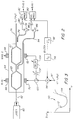
- Figure 3 is a plot of the modulator output power intensity I( ⁇ ) with respect to modulating voltage ⁇ .
- plot 110 illustrates, approximately linear operation as designated by dashed line 114 is provided at the quadrature operating points (e.g., point 112) of the modulator.
- the present invention maintains operation at or about the quadrature operating point 112, thereby reducing second order distortions, using a feedback arrangement in which a phase difference caused by the second order distortion is monitored and minimized.
- An optical carrier signal is provided by a laser 10.
- the optical carrier is communicated via an optical path 12 to a polarization transformer 14 that optimizes the orientation of the E field from the laser with respect to the crystal axis of a Mach Zehnder modulator 18.
- the polarization transformer 14 is coupled to Mach Zehnder modulator 18 via optical path 16 in a conventional manner.
- Mach Zehnder modulator 18 will modulate the optical carrier input thereto by a modulating signal applied at a modulating input 20.
- the resultant modulated carrier is output from the Mach Zehnder modulator via optical output path 22.
- the modulated optical carrier from the external modulator 18 is sampled via a coupler 24, that outputs the sampled light to a photodetector 26.
- Photodetector 26 converts the sampled energy into the electrical domain, where it is amplified by an amplifier 28 prior to input to a mixer 30.
- mixer 30 the sampled signal is mixed with a mixing frequency from synthesizer 32.
- synthesizer 32 outputs a 49.92 MHz periodic waveform.
- Synthesizer 32 is phase locked to a synthesizer 34, that in the illustrated embodiment outputs a 24.96 MHz signal.
- the 24.96 MHz signal is mixed in a mixer 36 with a pilot tone from oscillator 38 (e.g., 40 kHz) and passed through a bandpass filter 40 to provide a 25 MHz signal for input via tee 42 to input port 20 of external modulator 18. This 25 MHz signal will appear together with an information signal as modulation on the sampled optical carrier from the external modulator.
- the actual information signal to be carried on the optical carrier is input to the modulator 18 via an RF input terminal 54 and adder 56 in a conventional manner. Since the pilot tone used in connection with the second order phase comparison is well below the frequency of the desired information signal, the pilot tone does not interfere with the communication of the information signal.
- the 40 kHz pilot tone will be present in the signal in the electrical domain input to mixer 30 from amplifier 28.
- the second order distortion of the 40 kHz pilot tone appearing at 80 kHz, will be output from mixer 30.
- a low pass filter 44 limits the output from mixer 30 to the desired 80 kHz component, for input to a phase comparator 46.
- a frequency doubler 52 doubles the original 40 kHz pilot tone from oscillator 38 to provide an 80 kHz output for comparison with the 80 kHz signal from low pass filter 44.
- Any phase difference between the two 80 kHz signals input to phase comparator 46 is determined, and output through an appropriate time delay 48 to an amplifier 50 for providing an error signal based on the phase difference.
- the error signal is input to tee 42, where it is combined with the 25 MHz output from bandpass filter 40 for input as a biasing signal to external modulator 18.
- Phase comparator 46 can comprise any conventional phase comparison circuit, such as a multiplier and a filter. Such phase comparators are well known in the art.
- the error signal provided by the apparatus of Figure 1 is indicative of a phase difference between the second harmonic of the pilot signal from frequency multiplier 52 and second order harmonics of the pilot signal present in the sampled modulated optical carrier from external modulator 18.
- the sign and magnitude of the error signal will inherently correspond to the magnitude and direction of the phase difference detected by the phase comparator 46.
- use of the error signal to bias external modulator 18 will tend to drive the phase difference to zero, by adjusting the operating point of the external modulator to quadrature. This has the effect of reducing second order distortions produced by the external modulator.
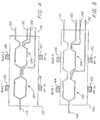
- the present invention can also be used to linearize the operation of cascaded external modulators.
- external modulator 64 comprises a pair of series coupled Mach Zehnder modulators 65, 67.
- Laser 60 is used to provide the optical carrier which is communicated to external modulator 64 via optical path 62.
- External modulator 64 contains separate bias inputs 66, 68 and separate modulating signal inputs 70, 72 for each of the Mach Zehnder modulators 65, 67, respectively.
- the outputs of modulators 65, 67 are sampled by optical paths 84, 76, respectively.
- the optical carrier modulated by modulator 64 is output via optical path 74 in a conventional manner.
- the information signal to be modulated by external modulator 64 is coupled via terminal 92 to an adder 94, where it is combined with a reference frequency (pilot tone) f s generated by oscillator 96.
- the combined signal is input via input port 70 to the first Mach Zehnder modulator 65.
- a splitter 100 is provided to divert a portion of the input signal to input port 72 of Mach Zehnder modulator 67 via a variable gain amplifier 102 and variable delay 104.
- Third order distortions produced by external modulator 64 can be reduced by adjusting the gain of amplifier 102 and delay 104 as well known in the art.
- the output from the first Mach Zehnder modulator 64 sampled via optical path 84 is input to a photodetector 86, amplified by an amplifier 88, and input to a signal processor 90 for comparison with the second harmonic of the pilot tone (2f s ) output from oscillator 98.
- Oscillators 98 and 96 are phase locked to enable signal processor 90 to provide an error signal indicative of the phase difference between the second harmonic of the pilot signal output from oscillator 98 and second order harmonics of the pilot signal present in the sampled modulated optical carrier output from Mach Zehnder modulator 65.
- Signal processor 90 can comprise, for example, a phase comparator, time delay, and amplifier as illustrated by components 46, 48 and 50 of Figure 1.
- bias 1 The error signal output from signal processor 90 ("bias 1") is input to bias port 66 of modulator 64. This bias voltage adjusts the bias of Mach Zehnder modulator 65 to minimize the phase difference between the second harmonic of the pilot signal and second order harmonics of the pilot signal present in the output sampled via optical path 84, thereby minimizing second order distortions produced by Mach Zehnder modulator 65.
- photodetector 78, amplifier 80, and signal processor 82 are used to compare the phase of the second order harmonics of the pilot signal present in the output of Mach Zehnder modulator 67 with the second harmonic of the pilot signal from oscillator 98, thereby producing an error signal ("bias 2") that is input to bias port 68 of external modulator 64. This minimizes second order distortions produced by Mach Zehnder modulator 67.
- Figures 4 and 5 illustrate alternative embodiments in which one or more directional couplers are used in an external modulator.
- external modulator 120 comprises a Mach Zehnder modulator 122 followed by a directional coupler 124. Separate bias and RF input ports 134, 138 are provided for Mach Zehnder modulator 122. Similarly, separate bias and RF input ports 136, 140 are provided for directional coupler 124.
- An optical carrier is input to the external modulator 120 via an optical path 118, and the modulated carrier is output from paths 130 and 132 provided by directional coupler 124.
- Second order distortions produced by Mach Zehnder modulator 122 are sampled via optical path 126. Second order distortions at the output of directional coupler 124 are sampled by optical path 128.
- the external modulator 120 of Figure 4 can be substituted for the external modulator 64 illustrated in Figure 2.
- Figure 5 illustrates an embodiment of an external modulator 150 that comprises two directional couplers 152, 154 coupled in series. Again, separate bias and RF input ports 164, 168 are provided for directional coupler 152 and separate bias and RF input ports 166, 170 are provided for directional coupler 154.
- the optical carrier is input to the external modulator 150 via optical path 148, and the modulated carrier is output from directional coupler 154 on optical paths 160 and 162. Sampling of the output of the first directional coupler 152 is provided by optical path 156. Sampling of the output of the second directional coupler 154 is provided by optical path 158.
- the external modulator 150 of Figure 5 can be substituted for modulator 64 of Figure 2.
- the present invention provides a method and apparatus for linearizing the operation of an external optical modulator, such as a balanced Mach Zehnder modulator.
- the invention takes advantage of the fact that second order distortion can be reduced by adjusting the modulator to operate at its quadrature bias point.
- a pilot signal is provided so that the phase difference between a second harmonic of the pilot signal and second order harmonics of the pilot signal present in the output of the modulator can be determined and minimized to maintain operation at or about the quadrature point.
- Additional feedback loops can be used for each of a plurality of external modulators operated in series. Independent adjustment of the series modulators enables effective reduction of the overall second order distortion provided by the external modulator.
Abstract
Description
- The present invention relates to optical modulators, and more specifically to a technique for linearizing the output of an external optical intensity modulator.
- Recently, there has been a growing interest in the development of analog, amplitude modulated optical communication systems. In comparison with digital systems, analog communication systems provide an efficient use of bandwidth. This is particularly useful in cable television (CATV) transmission system applications, where it is necessary to transmit a large number of video channels through an optical fiber. Compatibility with existing equipment is achieved by using the same signal format for optical transmission that is in use for coaxial cable signal transmission.
- In order to transmit an information signal (e.g., a television signal) over an optical fiber, a light beam ("carrier") must be modulated with the information signal. The "electrooptic effect" has been advantageously used to provide modulators for this purpose. For example, electrooptic modulators using miniature guiding structures are known which operate with a low modulating power.
- In electrooptic modulators, the electric field induced linear birefringence in an electrooptic material produces a change in the refractive index of the material which, in turn, impresses a phase modulation upon a light beam propagating through the material. The phase modulation is converted into intensity modulation by the addition of polarizers or optical circuitry. Ideally, an electrooptic modulator should have a linear relationship between its output optical power and the applied modulating voltage.
- In a "Mach Zehnder" type electrooptic modulator, an optical carrier (laser beam) is split into two paths. At least one path is electrically phase modulated. The two signals are then recombined in an interferometer to provide an intensity modulated carrier. Typically, lithium niobate (LiNbO₃) is used as the electrooptic material. Waveguides in such materials are readily formed by titanium indiffusion.
- The output power curve of a Mach Zehnder modulator is nonlinear. Practical analog optical communications systems, however, demand a high linearity. See, for example, W.I. Way, "Subcarrier Multiplexed Lightwave System Design Considerations for Subscriber Loop Applications", J. Lightwave Technol., Vol. 7, pp. 1806-1818 (1989). Modulator nonlinearities cause unacceptable harmonic and intermodulation distortions. When it is necessary to communicate a large number of channels, as in a CATV application, intermodulation distortions ("IMD") can impose serious limitations on the system performance.
- The problem of intermodulation distortions, and particularly second order distortion, is complicated by the fact that lithium niobate is an inherently unstable material. Thus, it is not possible to simply bias a Mach Zehnder modulator (e.g., to operate at its quadrature point) and then expect the modulator to continue to run at the desired operating point. In fact, the bias condition will dynamically change due to factors such as temperature, photorefractive instability, and displacement currents within the lithium niobate material. Thus, additional steps must be taken to ensure that the external modulator will run over time without an increase in second order distortion.
- It would be advantageous to provide a technique that dynamically tracks the second order distortion performance of an external optical modulator and maintains such performance at an acceptable level. It would be further advantageous to provide such a technique that can be used with a single optical modulator or a plurality of such modulators cascaded in series. The present invention provides a method and apparatus enjoying the aforementioned advantages.
- In accordance with the present invention, a method is provided for linearizing the operation of an external optical modulator. An optical carrier is modulated in the modulator by a pilot signal. The modulated optical carrier is sampled from the modulator. An error signal is generated which is indicative of a phase difference between a second harmonic of the pilot signal and second order harmonics of the pilot signal present in the sampled modulated optical carrier. The error signal is fed back to the modulator to adjust a bias thereof to minimize the phase difference and thereby minimize second order distortions produced by the modulator.
- In an illustrated embodiment, the pilot signal is mixed with an information signal (e.g., CATV signals) for modulation of the carrier in the modulator by both the pilot signal and the information signal. An embodiment is also disclosed wherein a plurality of external modulators are coupled in series. Each of the modulators receives a pilot signal for modulating the optical carrier. For each modulator, the modulated optical carrier output therefrom is sampled and an error signal is generated indicative of a phase difference between a second harmonic of the pilot signal input to the modulator and second order harmonics of the pilot signal present in the sampled modulated optical carrier. The error signal for each modulator is fed back to adjust the bias of the modulator and thereby minimize the phase difference between the second harmonic of the pilot signal and second order harmonics of the pilot signal present in the sampled modulated optical carrier. In this manner, second order distortions produced by the modulators are minimized.
- Apparatus in accordance with the present invention includes means for modulating an optical carrier signal by an information signal and a pilot signal. The modulated optical carrier signal is sampled from the modulating means, and an error signal is generated indicative of a phase difference between a second harmonic of the pilot signal and second order harmonics of the pilot signal present in the sampled modulated optical carrier signal. Means are provided for feeding the error signal back to the modulating means to adjust a bias thereof in order to minimize the phase difference. In this manner, second order distortions produced by the modulating means are minimized.
- In an illustrated embodiment, means are provided for mixing the information signal with the pilot signal for input to the modulating means as a combined signal to modulate the carrier. The modulating means can comprise a plurality of external modulators in series, each receiving the pilot signal at a modulating signal input thereof. Each modulator comprises means for sampling the modulated optical carrier from the modulator, means for generating an error signal indicative of a phase difference between a second harmonic of the pilot signal and second order harmonics of the pilot signal present in the sampled carrier, and means for feeding the error signal back to the modulator to adjust a bias thereof to minimize the phase difference.
- In an illustrated embodiment, the pilot signal comprises a first tone having a frequency fs. The means for generating the error signal comprise an oscillator providing a second tone having a frequency 2fs phase locked to the first tone. Means are provided for mixing the second tone with the sampled modulated optical carrier to recover second order harmonics of the first tone. Phase comparator means compare the phase of the second tone to the phase of the recovered second order harmonics. Means responsive to the phase comparator generate an error signal having a sign and magnitude that correspond to the magnitude and direction of a phase difference detected by the phase comparator means. In one embodiment, the modulator(s) comprises a Mach Zehnder modulator(s) having a separate bias input(s) for receiving the error signal. In another embodiment, the modulating means comprise a directional coupler. In an embodiment using series modulators, a Mach Zehnder modulator can be followed by a directional coupler. In an alternative arrangement, a first directional coupler can be followed by a second directional coupler. In either embodiment, the modulators can be provided with separate bias inputs for receiving the error signal. Further, the error signal for each modulator in a plurality thereof is preferably fed back to its respective modulator in a feedback loop that has a time constant which is shorter than that of the following modulator in the series of modulators.
-
- Figure 1 is a block diagram showing a first embodiment of the invention that uses a double heterodyne arrangement for providing an error signal to reduce second order distortions in a Mach Zehnder modulator;
- Figure 2 is a block diagram of an embodiment for reducing second order distortions produced by a pair of series coupled Mach Zehnder modulators;
- Figure 3 is a graph illustrating the quadrature operating point of an external modulator;
- Figure 4 is a schematic illustration of an embodiment wherein the external modulator comprises a Mach Zehnder modulator followed by a series coupled directional coupler; and
- Figure 5 is a schematic representation of an external modulator comprising a pair of series coupled directional couplers.
- External modulators used in connection with optical signal distribution systems must provide linear operation over a relatively large modulation range. However, such modulators typically produce rather large second order distortions, which must be reduced in order to allow the practical use of such modulators. Ideally, an external modulator (such as a Mach Zehnder modulator) should be operated at its quadrature operating point, where the most linear operation can be achieved. This is illustrated in Figure 3, which is a plot of the modulator output power intensity I(ν) with respect to modulating voltage ν. As
plot 110 illustrates, approximately linear operation as designated by dashedline 114 is provided at the quadrature operating points (e.g., point 112) of the modulator. - The present invention maintains operation at or about the
quadrature operating point 112, thereby reducing second order distortions, using a feedback arrangement in which a phase difference caused by the second order distortion is monitored and minimized. One embodiment of the invention is illustrated in Figure 1, in which an optical carrier signal is provided by a laser 10. The optical carrier is communicated via anoptical path 12 to apolarization transformer 14 that optimizes the orientation of the E field from the laser with respect to the crystal axis of a Mach Zehnder modulator 18. Thepolarization transformer 14 is coupled to Mach Zehnder modulator 18 viaoptical path 16 in a conventional manner. Mach Zehnder modulator 18 will modulate the optical carrier input thereto by a modulating signal applied at a modulatinginput 20. The resultant modulated carrier is output from the Mach Zehnder modulator viaoptical output path 22. - In accordance with the present invention, the modulated optical carrier from the
external modulator 18 is sampled via acoupler 24, that outputs the sampled light to aphotodetector 26.Photodetector 26 converts the sampled energy into the electrical domain, where it is amplified by anamplifier 28 prior to input to a mixer 30. In mixer 30, the sampled signal is mixed with a mixing frequency fromsynthesizer 32. In the specific embodiment shown,synthesizer 32 outputs a 49.92 MHz periodic waveform. -
Synthesizer 32 is phase locked to a synthesizer 34, that in the illustrated embodiment outputs a 24.96 MHz signal. The 24.96 MHz signal is mixed in amixer 36 with a pilot tone from oscillator 38 (e.g., 40 kHz) and passed through abandpass filter 40 to provide a 25 MHz signal for input viatee 42 to inputport 20 ofexternal modulator 18. This 25 MHz signal will appear together with an information signal as modulation on the sampled optical carrier from the external modulator. - The actual information signal to be carried on the optical carrier is input to the
modulator 18 via anRF input terminal 54 andadder 56 in a conventional manner. Since the pilot tone used in connection with the second order phase comparison is well below the frequency of the desired information signal, the pilot tone does not interfere with the communication of the information signal. - The 40 kHz pilot tone will be present in the signal in the electrical domain input to mixer 30 from
amplifier 28. Upon mixing this signal with the output of 49.92MHz synthesizer 32, the second order distortion of the 40 kHz pilot tone, appearing at 80 kHz, will be output from mixer 30. This result can be seen in that the second harmonic of the 25 MHz signal input to the modulator appears at 50 MHz, which when mixed with the 49.92 MHz signal fromsynthesizer 32 results in the desired 80 kHz output (50.00-49.92 MHz = 80 kHz). Alow pass filter 44 limits the output from mixer 30 to the desired 80 kHz component, for input to aphase comparator 46. - A
frequency doubler 52 doubles the original 40 kHz pilot tone fromoscillator 38 to provide an 80 kHz output for comparison with the 80 kHz signal fromlow pass filter 44. Any phase difference between the two 80 kHz signals input to phasecomparator 46 is determined, and output through anappropriate time delay 48 to anamplifier 50 for providing an error signal based on the phase difference. The error signal is input to tee 42, where it is combined with the 25 MHz output frombandpass filter 40 for input as a biasing signal toexternal modulator 18.Phase comparator 46 can comprise any conventional phase comparison circuit, such as a multiplier and a filter. Such phase comparators are well known in the art. - The error signal provided by the apparatus of Figure 1 is indicative of a phase difference between the second harmonic of the pilot signal from
frequency multiplier 52 and second order harmonics of the pilot signal present in the sampled modulated optical carrier fromexternal modulator 18. The sign and magnitude of the error signal will inherently correspond to the magnitude and direction of the phase difference detected by thephase comparator 46. Thus, use of the error signal to biasexternal modulator 18 will tend to drive the phase difference to zero, by adjusting the operating point of the external modulator to quadrature. This has the effect of reducing second order distortions produced by the external modulator. - The present invention can also be used to linearize the operation of cascaded external modulators. An example of such an embodiment is illustrated in Figure 2, wherein
external modulator 64 comprises a pair of series coupled Mach Zehnder modulators 65, 67.Laser 60 is used to provide the optical carrier which is communicated toexternal modulator 64 viaoptical path 62.External modulator 64 containsseparate bias inputs modulating signal inputs modulators optical paths modulator 64 is output viaoptical path 74 in a conventional manner. - The information signal to be modulated by
external modulator 64 is coupled viaterminal 92 to anadder 94, where it is combined with a reference frequency (pilot tone) fs generated byoscillator 96. The combined signal is input viainput port 70 to the first Mach Zehnder modulator 65. Asplitter 100 is provided to divert a portion of the input signal to inputport 72 of Mach Zehnder modulator 67 via avariable gain amplifier 102 andvariable delay 104. Third order distortions produced byexternal modulator 64 can be reduced by adjusting the gain ofamplifier 102 and delay 104 as well known in the art. - The output from the first Mach Zehnder modulator 64 sampled via
optical path 84 is input to aphotodetector 86, amplified by anamplifier 88, and input to asignal processor 90 for comparison with the second harmonic of the pilot tone (2fs) output fromoscillator 98.Oscillators signal processor 90 to provide an error signal indicative of the phase difference between the second harmonic of the pilot signal output fromoscillator 98 and second order harmonics of the pilot signal present in the sampled modulated optical carrier output from Mach Zehnder modulator 65.Signal processor 90 can comprise, for example, a phase comparator, time delay, and amplifier as illustrated bycomponents bias 1") is input to biasport 66 ofmodulator 64. This bias voltage adjusts the bias of Mach Zehnder modulator 65 to minimize the phase difference between the second harmonic of the pilot signal and second order harmonics of the pilot signal present in the output sampled viaoptical path 84, thereby minimizing second order distortions produced by Mach Zehnder modulator 65. - Similarly,
photodetector 78,amplifier 80, andsignal processor 82 are used to compare the phase of the second order harmonics of the pilot signal present in the output of Mach Zehnder modulator 67 with the second harmonic of the pilot signal fromoscillator 98, thereby producing an error signal ("bias 2") that is input to biasport 68 ofexternal modulator 64. This minimizes second order distortions produced by Mach Zehnder modulator 67. - By monitoring the outputs of both of the Mach Zehnder modulators in
external modulator 64, and adjusting the respective biases, the second order distortions produced overall byexternal modulator 64 can be minimized. - Figures 4 and 5 illustrate alternative embodiments in which one or more directional couplers are used in an external modulator. In the embodiment illustrated in Figure 4,
external modulator 120 comprises a Mach Zehnder modulator 122 followed by adirectional coupler 124. Separate bias andRF input ports 134, 138 are provided for Mach Zehnder modulator 122. Similarly, separate bias andRF input ports directional coupler 124. An optical carrier is input to theexternal modulator 120 via anoptical path 118, and the modulated carrier is output frompaths directional coupler 124. Second order distortions produced by Mach Zehnder modulator 122 are sampled viaoptical path 126. Second order distortions at the output ofdirectional coupler 124 are sampled byoptical path 128. Theexternal modulator 120 of Figure 4 can be substituted for theexternal modulator 64 illustrated in Figure 2. - Figure 5 illustrates an embodiment of an
external modulator 150 that comprises twodirectional couplers RF input ports 164, 168 are provided fordirectional coupler 152 and separate bias andRF input ports directional coupler 154. The optical carrier is input to theexternal modulator 150 viaoptical path 148, and the modulated carrier is output fromdirectional coupler 154 onoptical paths directional coupler 152 is provided by optical path 156. Sampling of the output of the seconddirectional coupler 154 is provided byoptical path 158. Theexternal modulator 150 of Figure 5 can be substituted formodulator 64 of Figure 2. - It should now be appreciated that the present invention provides a method and apparatus for linearizing the operation of an external optical modulator, such as a balanced Mach Zehnder modulator. The invention takes advantage of the fact that second order distortion can be reduced by adjusting the modulator to operate at its quadrature bias point. A pilot signal is provided so that the phase difference between a second harmonic of the pilot signal and second order harmonics of the pilot signal present in the output of the modulator can be determined and minimized to maintain operation at or about the quadrature point. Additional feedback loops can be used for each of a plurality of external modulators operated in series. Independent adjustment of the series modulators enables effective reduction of the overall second order distortion provided by the external modulator.
- Although the invention has been described in connection with various specific embodiments thereof, those skilled in the art will appreciate that numerous adaptations and modifications may be made thereto without departing from the spirit and scope of the invention as set forth in the claims.
Claims (15)
- A method for linearizing the operation of an external optical modulator comprising the steps of:
modulating an optical carrier in said modulator by a pilot signal;
sampling said modulated optical carrier from said modulator;
generating an error signal indicative of a phase difference between a second harmonic of said pilot signal and second order harmonics of said pilot signal present in said sampled modulated optical carrier; and
feeding said error signal back to said modulator to adjust a bias thereof to minimize said phase difference and thereby minimize second order distortions produced by said modulator. - A method in accordance with claim 1 comprising the further step of:
mixing said pilot signal with an information signal for modulation of said carrier in said modulator. - A method in accordance with claim 1 comprising the further steps of:
providing a plurality of external modulators in series, each of said modulators receiving said pilot signal for modulating said optical carrier and, for each of said modulators:
sampling the modulated optical carrier from the modulator;
generating an error signal indicative of a phase difference between a second harmonic of said pilot signal and second order harmonics of said pilot signal present in the sampled modulated optical carrier; and
feeding said error signal back to said modulator to adjust a bias thereof to minimize said phase difference and thereby minimize second order distortions produced by said modulator. - Linearized external optical modulator apparatus comprising:
means for modulating an optical carrier signal by an information signal and a pilot signal;
means for sampling the modulated optical carrier signal from said modulating means;
means for generating an error signal indicative of a phase difference between a second harmonic of said pilot signal and second order harmonics of said pilot signal present in said sampled modulated optical carrier signal; and
means for feeding said error signal back to said modulating means to adjust a bias thereof to minimize said phase difference and thereby minimize second order distortions produced by said modulating means. - Apparatus in accordance with claim 4 further comprising:
means for mixing said information signal with said pilot signal for input to said modulating means as a combined signal to modulate said carrier. - Apparatus in accordance with claim 4 wherein said modulating means comprise:
a plurality of external modulators in series, each of said modulators receiving said pilot signal at a modulating signal input thereof and, for each modulator:
means for sampling the modulated optical carrier from the modulator;
means for generating an error signal indicative of a phase difference between a second harmonic of said pilot signal and second order harmonics of said pilot signal present in the sampled carrier from the modulator; and
means for feeding said error signal back to the modulator to adjust a bias thereof to minimize said phase difference. - Apparatus in accordance with one of claims 4 to 6 wherein:
said pilot signal comprises a first tone having a frequency fs; and
said means for generating said error signal comprise:
an oscillator providing a second tone having a frequency 2fs phase locked to said first tone,
means for mixing said second tone with said sampled modulated optical carrier to recover second order harmonics of said first tone;
phase comparator means for comparing the phase of said second tone to the phase of said recovered second order harmonics; and
means responsive to said phase comparator means for generating an error signal having a sign and magnitude that correspond to the direction and magnitude of a phase difference detected by said phase comparator means. - Apparatus in accordance with one of claims 4 to 7 wherein said modulating means comprise Mach Zehnder modulators.
- Apparatus in accordance with claim 8 wherein said Mach Zehnder modulators have separate bias inputs for receiving said error signal.
- Apparatus in accordance with one of claims 6 to 9 wherein the error signal for each modulator in said plurality is fed back to its respective modulator in a feedback loop that has a time constant which is shorter than that of the following modulator in said series.
- Apparatus in accordance with one of claims 4 to 7 wherein said modulating means comprise a directional coupler.
- Apparatus in accordance with one of claims 6 to 10 wherein said series modulators comprise a Mach Zehnder modulator followed by a directional coupler.
- Apparatus in accordance with claim 12 wherein said Mach Zehnder modulator and directional coupler each have a separate bias input for receiving said error signal.
- Apparatus in accordance with one of claims 6 or 7 wherein each of said modulators comprises a directional coupler.
- Apparatus in accordance with claim 14 wherein said directional couplers have separate bias inputs for receiving said error signal.
Applications Claiming Priority (2)
| Application Number | Priority Date | Filing Date | Title |
|---|---|---|---|
| US963460 | 1992-10-20 | ||
| US07/963,460 US5321543A (en) | 1992-10-20 | 1992-10-20 | Apparatus and method for linearizing an external optical modulator |
Publications (2)
| Publication Number | Publication Date |
|---|---|
| EP0594088A1 true EP0594088A1 (en) | 1994-04-27 |
| EP0594088B1 EP0594088B1 (en) | 1998-12-09 |
Family
ID=25507277
Family Applications (1)
| Application Number | Title | Priority Date | Filing Date |
|---|---|---|---|
| EP93116752A Expired - Lifetime EP0594088B1 (en) | 1992-10-20 | 1993-10-16 | Apparatus and method for linearizing an external optical modulator |
Country Status (9)
| Country | Link |
|---|---|
| US (1) | US5321543A (en) |
| EP (1) | EP0594088B1 (en) |
| AU (1) | AU658806B2 (en) |
| DE (1) | DE69322479T2 (en) |
| ES (1) | ES2125292T3 (en) |
| GR (1) | GR3029420T3 (en) |
| MX (1) | MX9306511A (en) |
| NZ (1) | NZ248982A (en) |
| TW (1) | TW256884B (en) |
Cited By (6)
| Publication number | Priority date | Publication date | Assignee | Title |
|---|---|---|---|---|
| GB2293022A (en) * | 1994-09-07 | 1996-03-13 | Toshiba Kk | Controlling optical modulators |
| EP0768765A1 (en) * | 1995-10-12 | 1997-04-16 | PIRELLI CAVI S.p.A. | Bias system in an optical CATV modulator |
| FR2740285A1 (en) * | 1995-10-23 | 1997-04-25 | Alcatel Submarcom | ELECTRO-ABSORPTION MODULATOR AMPLITUDE MODULATION DEVICE |
| EP0782282A3 (en) * | 1995-12-29 | 2000-10-11 | AT&T Corp. | Synchronous polarization and phase modulation using a periodic waveform with complex harmonics for improved perfomance of optical transmission systems |
| EP1727303A2 (en) * | 2005-05-23 | 2006-11-29 | Fujitsu Limited | Optical transmitting apparatus, optical receiving apparatus, and optical communication system comprising them |
| US11719963B2 (en) | 2020-04-29 | 2023-08-08 | Lightelligence, Inc. | Optical modulation for optoelectronic processing |
Families Citing this family (68)
| Publication number | Priority date | Publication date | Assignee | Title |
|---|---|---|---|---|
| US5473460A (en) * | 1994-07-25 | 1995-12-05 | At&T Corp. | Adaptive equalizer for analog optical signal transmission |
| JP2697639B2 (en) * | 1994-11-04 | 1998-01-14 | 日本電気株式会社 | Light modulator |
| US5526158A (en) * | 1994-12-22 | 1996-06-11 | Trw Inc. | Low-bias heterodyne fiber-optic communication link |
| US5488503A (en) * | 1995-02-09 | 1996-01-30 | Hughes Aircraft Company | Low-power, stabilized, photonic modulator system |
| US5710653A (en) * | 1995-03-06 | 1998-01-20 | Fiber Optic Network Solutions Corp. | Linear multi-output optical transmitter system |
| US5875048A (en) * | 1995-03-06 | 1999-02-23 | Cfx Communication Systems,Llc | Linear multi-output optical transmitter system |
| US6233077B1 (en) | 1995-05-11 | 2001-05-15 | Ciena Corporation | Remodulating channel selectors for WDM optical communication systems |
| US9191117B2 (en) * | 1995-05-11 | 2015-11-17 | Ciena Corporation | High-speed optical transponder systems |
| US5504609A (en) * | 1995-05-11 | 1996-04-02 | Ciena Corporation | WDM optical communication system with remodulators |
| GB2308252B (en) * | 1995-12-16 | 2000-02-23 | Northern Telecom Ltd | WDM channel insertion |
| US5953139A (en) * | 1996-03-06 | 1999-09-14 | Cfx Communications Systems, Llc | Wavelength division multiplexing system |
| US5781327A (en) * | 1996-08-19 | 1998-07-14 | Trw Inc. | Optically efficient high dynamic range electro-optic modulator |
| US6052393A (en) * | 1996-12-23 | 2000-04-18 | The Regents Of The University Of Michigan | Broadband Sagnac Raman amplifiers and cascade lasers |
| US6111680A (en) * | 1997-12-01 | 2000-08-29 | Ebara Corporation | Transmitting a signal using duty cycle modulation |
| US6374006B1 (en) | 1998-03-20 | 2002-04-16 | Xtera Communications, Inc. | Chirped period gratings for raman amplification in circulator loop cavities |
| US6693737B2 (en) | 1998-03-24 | 2004-02-17 | Xtera Communications, Inc. | Dispersion compensating nonlinear polarization amplifiers |
| US6600592B2 (en) | 1998-03-24 | 2003-07-29 | Xtera Communications, Inc. | S+ band nonlinear polarization amplifiers |
| US6356384B1 (en) | 1998-03-24 | 2002-03-12 | Xtera Communications Inc. | Broadband amplifier and communication system |
| US6760148B2 (en) | 1998-03-24 | 2004-07-06 | Xtera Communications, Inc. | Nonlinear polarization amplifiers in nonzero dispersion shifted fiber |
| US6574037B2 (en) | 1998-06-16 | 2003-06-03 | Xtera Communications, Inc. | All band amplifier |
| US6985283B1 (en) | 1998-06-16 | 2006-01-10 | Xtera Communications, Inc. | Fiber-optic compensation for dispersion, gain tilt, and band pump nonlinearity |
| US6359725B1 (en) | 1998-06-16 | 2002-03-19 | Xtera Communications, Inc. | Multi-stage optical amplifier and broadband communication system |
| US6335820B1 (en) | 1999-12-23 | 2002-01-01 | Xtera Communications, Inc. | Multi-stage optical amplifier and broadband communication system |
| US6885498B2 (en) | 1998-06-16 | 2005-04-26 | Xtera Communications, Inc. | Multi-stage optical amplifier and broadband communication system |
| US6014241A (en) * | 1998-06-25 | 2000-01-11 | Tacan Corporation | Method and apparatus for reducing non-linear characteristics of a signal modulator by cross-correlation |
| US6426822B1 (en) * | 1998-06-25 | 2002-07-30 | Ipicom, Inc. | Method and apparatus for reducing non-linear characteristics of a signal modulator by coherent data collection |
| US6567430B1 (en) | 1998-09-21 | 2003-05-20 | Xtera Communications, Inc. | Raman oscillator including an intracavity filter and amplifiers utilizing same |
| US7016607B1 (en) | 1998-12-14 | 2006-03-21 | Tellabs Operations, Inc. | Methods and apparatus for optical network management using pilot tones |
| GB9827602D0 (en) * | 1998-12-15 | 1999-02-10 | Northern Telecom Ltd | Optical equaliser |
| US6479979B1 (en) | 1999-07-09 | 2002-11-12 | Srico, Inc. | Opto-electric device for measuring the root-mean-square value of an alternating current voltage |
| DE60139923D1 (en) | 2000-01-12 | 2009-10-29 | Xtera Comm Inc | TWO-SIDED PUMP RAMA AMPLIFIER |
| AU2001264548A1 (en) | 2000-02-14 | 2001-10-23 | Xtera Communications, Inc. | Nonlinear optical loop mirror |
| US6931214B1 (en) * | 2000-05-10 | 2005-08-16 | Tellabs Operations, Inc. | Method and apparatus for maintaining a pre-determined ratio of a pilot tone power and a mean optical output power of an optical signal |
| US7173551B2 (en) * | 2000-12-21 | 2007-02-06 | Quellan, Inc. | Increasing data throughput in optical fiber transmission systems |
| US7149256B2 (en) | 2001-03-29 | 2006-12-12 | Quellan, Inc. | Multilevel pulse position modulation for efficient fiber optic communication |
| US7307569B2 (en) | 2001-03-29 | 2007-12-11 | Quellan, Inc. | Increasing data throughput in optical fiber transmission systems |
| DE60238602D1 (en) | 2001-04-04 | 2011-01-27 | Quellan Inc | METHOD AND SYSTEM FOR DECODING MULTI-LEVEL SIGNALS |
| US7085500B2 (en) * | 2001-04-30 | 2006-08-01 | Lockheed Martin Corp. | Programmable optical vector modulator and method for use in coherent optical communications |
| US20030030873A1 (en) * | 2001-05-09 | 2003-02-13 | Quellan, Inc. | High-speed adjustable multilevel light modulation |
| WO2003012535A1 (en) * | 2001-07-27 | 2003-02-13 | Axe, Inc. | Optical pulse generator with single frequency drive |
| WO2003071731A1 (en) | 2002-02-15 | 2003-08-28 | Quellan, Inc. | Multi-level signal clock recovery technique |
| WO2003077423A2 (en) * | 2002-03-08 | 2003-09-18 | Quellan, Inc. | High speed analog-to-digital converter using a unique gray code having minimal bit transitions |
| JP3881270B2 (en) * | 2002-03-26 | 2007-02-14 | 富士通株式会社 | Drive control device and drive control method for optical modulator |
| AU2003223687A1 (en) * | 2002-04-23 | 2003-11-10 | Quellan, Inc. | Combined ask/dpsk modulation system |
| JP2004013681A (en) * | 2002-06-10 | 2004-01-15 | Bosu & K Consulting Kk | Name card information managing system |
| US7035361B2 (en) * | 2002-07-15 | 2006-04-25 | Quellan, Inc. | Adaptive noise filtering and equalization for optimal high speed multilevel signal decoding |
| AU2003287628A1 (en) * | 2002-11-12 | 2004-06-03 | Quellan, Inc. | High-speed analog-to-digital conversion with improved robustness to timing uncertainty |
| US7804760B2 (en) | 2003-08-07 | 2010-09-28 | Quellan, Inc. | Method and system for signal emulation |
| DE112004001455B4 (en) * | 2003-08-07 | 2020-04-23 | Intersil Americas LLC | Cross-talk cancellation method and system |
| US7366428B2 (en) * | 2003-09-16 | 2008-04-29 | Sumitomo Electric Indutries, Ltd. | Optical receiver |
| JP4510832B2 (en) * | 2003-11-17 | 2010-07-28 | ケラン インコーポレイテッド | Method and system for antenna interference cancellation |
| US7616700B2 (en) | 2003-12-22 | 2009-11-10 | Quellan, Inc. | Method and system for slicing a communication signal |
| US7522883B2 (en) * | 2004-12-14 | 2009-04-21 | Quellan, Inc. | Method and system for reducing signal interference |
| US7725079B2 (en) | 2004-12-14 | 2010-05-25 | Quellan, Inc. | Method and system for automatic control in an interference cancellation device |
| US7773695B2 (en) * | 2005-08-19 | 2010-08-10 | Dominic Kotab | Amplitude modulator |
| US20070092262A1 (en) * | 2005-10-25 | 2007-04-26 | Donald Bozarth | Adaptive optical transmitter for use with externally modulated lasers |
| US8532499B2 (en) * | 2005-10-25 | 2013-09-10 | Emcore Corporation | Optical transmitter with adaptively controlled optically linearized modulator |
| US7853155B2 (en) * | 2005-12-12 | 2010-12-14 | Emcore Corporation | Method for adjusting bias in optical transmitter with external modulator |
| US7463802B2 (en) * | 2006-01-13 | 2008-12-09 | Emcore Corporation | Integrated circuit for adjusting bias in optical transmitter with external modulator |
| US7499603B1 (en) | 2006-01-19 | 2009-03-03 | Lockheed Martin Corporation | Range extended electrooptic modulator |
| WO2007127369A2 (en) | 2006-04-26 | 2007-11-08 | Quellan, Inc. | Method and system for reducing radiated emissions from a communications channel |
| WO2009054883A1 (en) * | 2007-10-19 | 2009-04-30 | Lightwire, Inc. | Silicon-based optical modulator for analog applications |
| CN102393574B (en) * | 2011-05-24 | 2015-07-22 | 中兴通讯股份有限公司 | Phase compensation device and method of pilot signals of lithium niobate modulator |
| FR3002654A1 (en) | 2013-02-26 | 2014-08-29 | St Microelectronics Sa | OPTICAL MODULATOR WITH AUTOMATIC POLARIZATION CORRECTION |
| US9705599B2 (en) * | 2015-07-30 | 2017-07-11 | Google Inc. | Systems for improved spectral efficiency in multi-carrier communication systems |
| TWI641881B (en) | 2016-02-19 | 2018-11-21 | 光聯通訊有限公司 | An optical transmitter with mach-zehnder modulator and method for operating the same |
| WO2018042422A1 (en) * | 2016-08-29 | 2018-03-08 | Technion Research And Development Foundation Ltd. | Electro-optical system |
| US11018773B1 (en) * | 2018-10-26 | 2021-05-25 | United States Of America As Represented By The Administrator Of National Aeronautics And Space Administration | Cascaded offset optical modulator for optical communications |
Citations (3)
| Publication number | Priority date | Publication date | Assignee | Title |
|---|---|---|---|---|
| EP0407919A2 (en) * | 1989-07-11 | 1991-01-16 | Harmonic Lightwaves, Inc. | Optical transmitters linearized by means of parametric feedback |
| EP0448832A2 (en) * | 1990-03-29 | 1991-10-02 | Hughes Aircraft Company | Automatic bias controller for electro-optic modulator |
| JPH04294318A (en) * | 1991-03-25 | 1992-10-19 | Mitsubishi Electric Corp | Automatic control circuit for optical modulator bias |
Family Cites Families (5)
| Publication number | Priority date | Publication date | Assignee | Title |
|---|---|---|---|---|
| JPS59182637A (en) * | 1983-03-31 | 1984-10-17 | Matsushita Electric Ind Co Ltd | Optical transmitter of video signal |
| US5161044A (en) * | 1989-07-11 | 1992-11-03 | Harmonic Lightwaves, Inc. | Optical transmitters linearized by means of parametric feedback |
| US5077619A (en) * | 1989-10-25 | 1991-12-31 | Tacan Corporation | High linearity optical transmitter |
| US5132829A (en) * | 1989-12-18 | 1992-07-21 | Bell Telephone Laboratories Inc. | Tone spacing and power level monitor for fsk lightwave systems |
| US5166509A (en) * | 1990-11-09 | 1992-11-24 | Tacan Corporation | Optical modulator noise nonlinearity reduction circuit |
-
1992
- 1992-10-20 US US07/963,460 patent/US5321543A/en not_active Expired - Lifetime
-
1993
- 1993-10-16 EP EP93116752A patent/EP0594088B1/en not_active Expired - Lifetime
- 1993-10-16 TW TW082108592A patent/TW256884B/zh not_active IP Right Cessation
- 1993-10-16 DE DE69322479T patent/DE69322479T2/en not_active Expired - Fee Related
- 1993-10-16 ES ES93116752T patent/ES2125292T3/en not_active Expired - Lifetime
- 1993-10-18 NZ NZ248982A patent/NZ248982A/en not_active IP Right Cessation
- 1993-10-18 AU AU49075/93A patent/AU658806B2/en not_active Ceased
- 1993-10-20 MX MX9306511A patent/MX9306511A/en not_active IP Right Cessation
-
1999
- 1999-02-17 GR GR990400503T patent/GR3029420T3/en unknown
Patent Citations (3)
| Publication number | Priority date | Publication date | Assignee | Title |
|---|---|---|---|---|
| EP0407919A2 (en) * | 1989-07-11 | 1991-01-16 | Harmonic Lightwaves, Inc. | Optical transmitters linearized by means of parametric feedback |
| EP0448832A2 (en) * | 1990-03-29 | 1991-10-02 | Hughes Aircraft Company | Automatic bias controller for electro-optic modulator |
| JPH04294318A (en) * | 1991-03-25 | 1992-10-19 | Mitsubishi Electric Corp | Automatic control circuit for optical modulator bias |
Non-Patent Citations (3)
| Title |
|---|
| PATENT ABSTRACTS OF JAPAN vol. 17, no. 105 (P - 1495) 3 March 1993 (1993-03-03) * |
| V.A. O'BYRNE ET AL: "Analysis and measurement of interferometric distortion products produced in externally modulated AM video systems", OPTICAL FIBER COMMUNICATION CONFERENCE OFC'91, no. TUC5, 19 February 1991 (1991-02-19), SAN DIEGO, CALIFORNIA,US, pages 11, XP000270321 * |
| YU WANG-BOULIC: "A Linearized Optical Modulator for Reducing Third-order Intermodulation Distortion", JOURNAL OF LIGHTWAVE TECHNOLOGY., vol. 10, no. 8, August 1992 (1992-08-01), NEW YORK US, pages 1066 - 1070, XP000288345, DOI: doi:10.1109/50.136088 * |
Cited By (13)
| Publication number | Priority date | Publication date | Assignee | Title |
|---|---|---|---|---|
| GB2293022B (en) * | 1994-09-07 | 1997-01-08 | Toshiba Kk | External optical modulator |
| GB2293022A (en) * | 1994-09-07 | 1996-03-13 | Toshiba Kk | Controlling optical modulators |
| US5812297A (en) * | 1995-10-12 | 1998-09-22 | Pirelli Cavi S.P.A. | Bias system in an optical CATV modulator |
| EP0768765A1 (en) * | 1995-10-12 | 1997-04-16 | PIRELLI CAVI S.p.A. | Bias system in an optical CATV modulator |
| FR2740285A1 (en) * | 1995-10-23 | 1997-04-25 | Alcatel Submarcom | ELECTRO-ABSORPTION MODULATOR AMPLITUDE MODULATION DEVICE |
| US5724178A (en) * | 1995-10-23 | 1998-03-03 | Alcatel Submarine Networks | Amplitude modulation circuit having an electro-absorption modulator |
| EP0771089A1 (en) * | 1995-10-23 | 1997-05-02 | Alcatel Submarine Networks | Amplitude modulation device with an electro-absorption modulator |
| EP0782282A3 (en) * | 1995-12-29 | 2000-10-11 | AT&T Corp. | Synchronous polarization and phase modulation using a periodic waveform with complex harmonics for improved perfomance of optical transmission systems |
| EP1727303A2 (en) * | 2005-05-23 | 2006-11-29 | Fujitsu Limited | Optical transmitting apparatus, optical receiving apparatus, and optical communication system comprising them |
| EP1727303A3 (en) * | 2005-05-23 | 2007-03-07 | Fujitsu Limited | Optical transmitting apparatus, optical receiving apparatus, and optical communication system comprising them |
| US7817923B2 (en) | 2005-05-23 | 2010-10-19 | Fujitsu Limited | Optical transmitting apparatus, optical receiving apparatus, and optical communication system comprising them |
| US8867927B2 (en) | 2005-05-23 | 2014-10-21 | Fujitsu Limited | Optical transmitting apparatus, optical receiving apparatus, and optical communication system comprising them |
| US11719963B2 (en) | 2020-04-29 | 2023-08-08 | Lightelligence, Inc. | Optical modulation for optoelectronic processing |
Also Published As
| Publication number | Publication date |
|---|---|
| US5321543A (en) | 1994-06-14 |
| AU4907593A (en) | 1994-05-05 |
| NZ248982A (en) | 1995-08-28 |
| DE69322479T2 (en) | 1999-06-24 |
| TW256884B (en) | 1995-09-11 |
| AU658806B2 (en) | 1995-04-27 |
| EP0594088B1 (en) | 1998-12-09 |
| ES2125292T3 (en) | 1999-03-01 |
| GR3029420T3 (en) | 1999-05-28 |
| MX9306511A (en) | 1994-04-29 |
| DE69322479D1 (en) | 1999-01-21 |
Similar Documents
| Publication | Publication Date | Title |
|---|---|---|
| US5321543A (en) | Apparatus and method for linearizing an external optical modulator | |
| US5109441A (en) | Fiber optic external modulator | |
| US5168534A (en) | Cascaded optic modulator arrangement | |
| EP0484791B1 (en) | Apparatus and method for externally modulating an optical carrier | |
| US6046838A (en) | Automatic bias control for electro-optic modulators | |
| US5031235A (en) | Cable system incorporating highly linear optical modulator | |
| US5850305A (en) | Adaptive predistortion control for optical external modulation | |
| US5532857A (en) | Wide dynamic range optical link using DSSC linearizer | |
| US5101450A (en) | Quadrature optical phase modulators for lightwave systems | |
| US5400417A (en) | Electro-optic modulator having gated-dither bias control | |
| EP0768765B1 (en) | Bias system in an optical CATV modulator | |
| US5239401A (en) | Optical modulator for cancellation of second-order intermodulation products in lightwave systems | |
| US4769853A (en) | High dynamic range fiber optical link | |
| US6211996B1 (en) | Angle modulator | |
| US6392779B1 (en) | Composite second-order bias control schemes | |
| US5040865A (en) | Frequency multiplying electro-optic modulator configuration and method | |
| WO2002082693A1 (en) | Optical linearizer for fiber communications | |
| US6917455B2 (en) | Cascaded RZ and NRZ laser modulators having RZ/NRZ phase alignment bias control | |
| US6539038B1 (en) | Reference frequency quadrature phase-based control of drive level and DC bias of laser modulator | |
| Liu et al. | In search of a linear electrooptic amplitude modulator | |
| JP4577945B2 (en) | Angle modulator | |
| US20030076570A1 (en) | Method, system and apparatus for optically receiving information | |
| JP2001159750A (en) | Optical transmitter and optical modulator | |
| US20020080454A1 (en) | Method, system and apparatus for optically transferring information |
Legal Events
| Date | Code | Title | Description |
|---|---|---|---|
| PUAI | Public reference made under article 153(3) epc to a published international application that has entered the european phase |
Free format text: ORIGINAL CODE: 0009012 |
|
| AK | Designated contracting states |
Kind code of ref document: A1 Designated state(s): DE ES FR GB GR |
|
| RAP1 | Party data changed (applicant data changed or rights of an application transferred) |
Owner name: GI CORPORATION |
|
| RAP1 | Party data changed (applicant data changed or rights of an application transferred) |
Owner name: GENERAL INSTRUMENT CORPORATION OF DELAWARE |
|
| 17P | Request for examination filed |
Effective date: 19941014 |
|
| 17Q | First examination report despatched |
Effective date: 19960705 |
|
| GRAG | Despatch of communication of intention to grant |
Free format text: ORIGINAL CODE: EPIDOS AGRA |
|
| GRAG | Despatch of communication of intention to grant |
Free format text: ORIGINAL CODE: EPIDOS AGRA |
|
| GRAH | Despatch of communication of intention to grant a patent |
Free format text: ORIGINAL CODE: EPIDOS IGRA |
|
| GRAH | Despatch of communication of intention to grant a patent |
Free format text: ORIGINAL CODE: EPIDOS IGRA |
|
| RAP1 | Party data changed (applicant data changed or rights of an application transferred) |
Owner name: NEXTLEVEL SYSTEMS, INC. |
|
| RAP1 | Party data changed (applicant data changed or rights of an application transferred) |
Owner name: GENERAL INSTRUMENT CORPORATION |
|
| GRAA | (expected) grant |
Free format text: ORIGINAL CODE: 0009210 |
|
| AK | Designated contracting states |
Kind code of ref document: B1 Designated state(s): DE ES FR GB GR |
|
| REF | Corresponds to: |
Ref document number: 69322479 Country of ref document: DE Date of ref document: 19990121 |
|
| REG | Reference to a national code |
Ref country code: ES Ref legal event code: FG2A Ref document number: 2125292 Country of ref document: ES Kind code of ref document: T3 |
|
| ET | Fr: translation filed | ||
| PLBE | No opposition filed within time limit |
Free format text: ORIGINAL CODE: 0009261 |
|
| STAA | Information on the status of an ep patent application or granted ep patent |
Free format text: STATUS: NO OPPOSITION FILED WITHIN TIME LIMIT |
|
| 26N | No opposition filed | ||
| REG | Reference to a national code |
Ref country code: GB Ref legal event code: IF02 |
|
| PGFP | Annual fee paid to national office [announced via postgrant information from national office to epo] |
Ref country code: DE Payment date: 20081201 Year of fee payment: 16 |
|
| PGFP | Annual fee paid to national office [announced via postgrant information from national office to epo] |
Ref country code: ES Payment date: 20081027 Year of fee payment: 16 |
|
| PGFP | Annual fee paid to national office [announced via postgrant information from national office to epo] |
Ref country code: GR Payment date: 20081031 Year of fee payment: 16 |
|
| PG25 | Lapsed in a contracting state [announced via postgrant information from national office to epo] |
Ref country code: DE Free format text: LAPSE BECAUSE OF NON-PAYMENT OF DUE FEES Effective date: 20100501 |
|
| PG25 | Lapsed in a contracting state [announced via postgrant information from national office to epo] |
Ref country code: GR Free format text: LAPSE BECAUSE OF NON-PAYMENT OF DUE FEES Effective date: 20100504 |
|
| PGFP | Annual fee paid to national office [announced via postgrant information from national office to epo] |
Ref country code: FR Payment date: 20101020 Year of fee payment: 18 |
|
| REG | Reference to a national code |
Ref country code: ES Ref legal event code: FD2A Effective date: 20110309 |
|
| PG25 | Lapsed in a contracting state [announced via postgrant information from national office to epo] |
Ref country code: ES Free format text: LAPSE BECAUSE OF NON-PAYMENT OF DUE FEES Effective date: 20110308 |
|
| PG25 | Lapsed in a contracting state [announced via postgrant information from national office to epo] |
Ref country code: ES Free format text: LAPSE BECAUSE OF NON-PAYMENT OF DUE FEES Effective date: 20091017 |
|
| REG | Reference to a national code |
Ref country code: FR Ref legal event code: ST Effective date: 20120629 |
|
| PG25 | Lapsed in a contracting state [announced via postgrant information from national office to epo] |
Ref country code: FR Free format text: LAPSE BECAUSE OF NON-PAYMENT OF DUE FEES Effective date: 20111102 |
|
| PGFP | Annual fee paid to national office [announced via postgrant information from national office to epo] |
Ref country code: GB Payment date: 20121010 Year of fee payment: 20 |
|
| REG | Reference to a national code |
Ref country code: GB Ref legal event code: PE20 Expiry date: 20131015 |
|
| PG25 | Lapsed in a contracting state [announced via postgrant information from national office to epo] |
Ref country code: GB Free format text: LAPSE BECAUSE OF EXPIRATION OF PROTECTION Effective date: 20131015 |