EP0593690B1 - Public telephone power consumption reducing method and device - Google Patents
Public telephone power consumption reducing method and device Download PDFInfo
- Publication number
- EP0593690B1 EP0593690B1 EP93903792A EP93903792A EP0593690B1 EP 0593690 B1 EP0593690 B1 EP 0593690B1 EP 93903792 A EP93903792 A EP 93903792A EP 93903792 A EP93903792 A EP 93903792A EP 0593690 B1 EP0593690 B1 EP 0593690B1
- Authority
- EP
- European Patent Office
- Prior art keywords
- microprocessor
- frequency
- handler
- inactive
- clock
- Prior art date
- Legal status (The legal status is an assumption and is not a legal conclusion. Google has not performed a legal analysis and makes no representation as to the accuracy of the status listed.)
- Expired - Lifetime
Links
Images
Classifications
-
- H—ELECTRICITY
- H04—ELECTRIC COMMUNICATION TECHNIQUE
- H04M—TELEPHONIC COMMUNICATION
- H04M17/00—Prepayment of wireline communication systems, wireless communication systems or telephone systems
- H04M17/02—Coin-freed or check-freed systems, e.g. mobile- or card-operated phones, public telephones or booths
- H04M17/023—Circuit arrangements
Definitions
- the present invention relates to the field of apparatus electrical including microprocessors, and particular a method and a device reducing their average consumption of electrical energy.
- EP-A-0 391 543 describes a microprocessor clock for a public telephone station, in which a microprocessor peripheral sends a switch simultaneously with the acceleration of the clock signal when a data packet is received from the telephone exchange.
- the interrupt is processed with the help of the accelerated clock signal to reduce the system response time, which reduces the normal clock frequency to save energy.
- This method has the disadvantage of relying excessively on the microprocessor device.
- controlling the power consumption of the microprocessor remains rudimentary. During the standby state, the microprocessor remains powered at normal frequency, this which induces a still relatively high consumption of electrical energy.
- EP-A-0 343 528 (D1) describes a system for a mobile telephone, one of which substantial reduction in energy can be achieved when switching off the clock frequency of the microprocessor during its idle phases.
- a first approach towards a finer control of the frequency of the microprocessor has been described in documents JP 3104360, JP 1119155 and JP 59200537. It consists in defining states in which the frequency must be at its maximum as well as states in which a reduced frequency can suffice.
- state means a period which lasts between a few seconds, by example to handle an incoming call, a few minutes when using the advanced phone functions such as the phone book.
- a major constraint of these solutions is to impose the processing of tasks evolved at maximum frequency. It should also be remembered that it is in these states that other consumers will intervene such as the coin acceptor, button lighting or display. This is why, the solutions proposed do not do not reduce the maximum energy consumed and only reduce average energy. However, when you are on a telephone line, it is well the maximum value which is decisive.
- the solution proposed here is based on the fact that the microprocessors consume mostly energy electric when switching pulses used to operate them. So if during periods of inactivity of a microprocessor on lower its clock frequency, then we decrease automatically consumes electrical energy.
- the main oscillator at the usual frequencies of 4 MHz, with a significant consumption (approximately 1 mA), the invention generally provides a system oscillators placed upstream of the clock manager, the whole being likely to vary the frequency clock reaching the microprocessor.
- the principle consists in entrusting the watch and the rhythm of switching between normal frequency and frequency secondary to a clock manager including a fixed time base, frequency still much lower than the secondary frequency chosen for the standby state of the microprocessor.
- the frequency of this fixed time base is dependent on the secondary frequency. If the normal operating frequency of the microprocessor is 4 MHz, the secondary frequency characteristic of the standby state is for example 250 kHz, and the frequency of the fixed time base is for example 50 Hz.
- a first line connects the manager to microprocessor and allows to send the pulses of fixed time base.
- the oscillator system consists of two oscillators, one, called the main oscillator, delivering the normal frequency, and the other one, says oscillator secondary, delivering the secondary frequency.
- the manager cuts power to oscillator main when the secondary oscillator, generating the secondary frequency of value lower than the frequency normal, is selected by the manager.
- the only signals remaining on the second line are those generated by the secondary oscillator.
- the normal frequency is 4 MHz and the secondary frequency of 250 KHz. In the case of a frequency divider, this secondary frequency is not other than the normal frequency divided by 16 by the manager.
- the transition to the active state can also be determined by the arrival of an interrupt which is itself the consequence of an external event: arrival of a tax impulse from the central, entry of a room into a slot, supply voltage monitoring, etc.
- the order communicated to the manager by the microprocessor depends on the activity of this microprocessor. he can decide to switch or stay on normal frequency if the need arises (e.g. timing a period such as the duration corresponding to a tax). When controls have determined the absence of timing, the microprocessor orders the manager to go to standby state.
- the manager varies the frequency. clock intermittently between values discreet. This achievement is different from a realization in which all the values of frequencies between a minimum and a maximum can a priori be chosen.
- the frequency can only take two values: the value of the normal frequency of the base of the microprocessor, called normal frequency, and a lower value, called secondary frequency, chosen to lower the power consumption of the microprocessor when conditions allow it to put in the inactive state.
- the oscillator system consists of a single oscillator, delivering the normal frequency, and the manager consists of a frequency divider.
- the circuits 5 controlled by the microprocessor 4 when it is in the active state, are connected to it by a bus address 15, known per se.
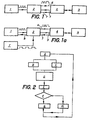
- Figure 2 shows a flowchart detailing the process where manager 2 goes to the normal frequency following an interrupt, then tries then switch back to the secondary frequency generating electrical energy savings.
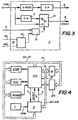
- FIG. 3 represents a block diagram of the clock manager 2 incorporating a frequency divider in the case of a single oscillator.
- This manager 2 is part of the specific integrated circuit of an application called ASIC.
- the oscillator 1 is connected to the manager 2 by the point CKIN, and delivers a fixed frequency of 4 MHz in the present example.
- the microprocessor 4 is connected to the manager 2 by the second line 6 which leads to the point CKOUT. Between these two points, the manager comprises, in this embodiment of the invention, a divider 11 of the frequency by a power N of 2, N possibly varying.
- the maximum value of N is determined by the minimum frequency at which the microprocessor 4. can operate normally.
- the selection between the two frequencies is made either by the third line 7 (carrying the command hereinafter called SPEED) or by recognizing an interrupt using a comparator 12 connected to the addresses AO to A15 of the address bus 15
- the reference 13 represents an OR function, consisting on the one hand of a type D flip-flop which stores the state of the comparator 12 (arrival of an interrupt) in synchronism with the execution of the internal orders of the microprocessor 4 , and on the other hand the specific control of the microprocessor 4 (line 7), these two conditions determining the position of the switch 14, and therefore the frequency conveyed by the line 6.
- the base frequency fixed time is 20 milliseconds.
- This base of fixed time is also part of the integrated circuit specific of an application called ASIC represented in the figure 3. It notably includes two dividers in cascade, one dividing by 4000, and the other by an integer P varying from 1 to 128.
- ASIC application specific of an application
- P varying from 1 to 128.
- N equal to 20.
- This value has the advantage of allowing the use of clock pulses to generate signals sent from the station's numeric keypad, when the station calls a telephone number formed by the user on the keyboard.
- Keyboard signals are made at a frequency can vary, in most countries, between a high value "HIGH”, corresponding to a period of 40 ms, and a low value "LOW", corresponding to a 60 ms period.
- a 16.6 ms time base is required to form a call number. This is the reason for the presence of a divider by P.
- the value of P is adjusted before delivery from the station. By the way, 20 ms is the maximum allowed to prevent the system from detection of parts introduced into the slot station payment does not lose coins entered immediately following each other.
- the telephone line delivers approximately 150 mW. More the frequencies used are low, or conversely high periods plus the smart part of the station is energy efficient and the more energy left can be stored in order, for example, to activate the magnets of the coin selector.
- Figure 4 shows schematically, on the logic plate of the station, the layout of the logic circuits 5 of Figure 1, with the connection of the different components by means of the address bus 15, represented by arrows wide, in the present exemplary embodiment. It goes from self lean arrows can also understand several conductors, or more generally several signal transmission means, for example by multiplexing.
- Address bus 15 connects the modem, meaning modulator-demodulator, the RTC, meaning Real Time Clock, the DTMF transceiver, meaning Dual Tone Multi Frequency, the CPU, meaning Central Processing Unit, memory M and I2C interface.
- the address bus 15, or taxiway includes addresses of most significant A8 to A15 and least significant addresses A0 to A7 from a demultiplexer (not shown). Every type of interrupt corresponds to an address, which allows in particular to manager 2, when an address corresponding to a switch appears on the bus address 15, to switch to normal frequency.
- a further reduction in frequency to 10 KHz or even less has a corresponding reduction of the electrical energy consumed by the microprocessor 4.
Landscapes
- Engineering & Computer Science (AREA)
- Computer Networks & Wireless Communication (AREA)
- Computer Security & Cryptography (AREA)
- Signal Processing (AREA)
- Power Sources (AREA)
- Prepayment Telephone Systems (AREA)
- Electrotherapy Devices (AREA)
- Microcomputers (AREA)
- Elimination Of Static Electricity (AREA)
- Telephone Set Structure (AREA)
- Feedback Control In General (AREA)
- Control Of Steam Boilers And Waste-Gas Boilers (AREA)
- Management Or Editing Of Information On Record Carriers (AREA)
- Preparation Of Compounds By Using Micro-Organisms (AREA)
- Manufacture, Treatment Of Glass Fibers (AREA)
- Input Circuits Of Receivers And Coupling Of Receivers And Audio Equipment (AREA)
- Communication Control (AREA)
Abstract
Description
La présente invention concerne le domaine des appareils électriques comprenant des microprocesseurs, et en particulier un procédé et un dispositif réduisant leur consommation moyenne d'énergie électrique.The present invention relates to the field of apparatus electrical including microprocessors, and particular a method and a device reducing their average consumption of electrical energy.
Pour certains appareils électriques, la nécessité de limiter la consommation d'énergie électrique à une valeur minimale est très importante. Ceci est particulièrement vrai pour les stations téléphoniques publiques. En effet, celles-ci sont généralement alimentées par la ligne téléphonique et l'énergie électrique autorisée qu'on peut prélever pour le fonctionnement est très limitée.For some electrical devices, the need to limit electrical energy consumption to a value minimal is very important. This is particularly true for public telephone stations. Indeed, these are generally supplied by the line telephone and the authorized electrical energy that we can charge for operation is very limited.
Le problème devient plus délicat au fur et à mesure que les stations téléphoniques publiques deviennent de plus en plus perfectionnées. The problem becomes more delicate as public telephone stations are becoming more sophisticated.
Le document EP-A- 0 275 566 décrit un procédé pour réduire la consommation électrique d'une station téléphonique publique, dans laquelle l'installation de commande comprend un microprocesseur. Dans ce procédé, la fréquence du cycle de base du système, commandée extérieurement, se trouve coupée par le microprocesseur au moyen d'un signal de coupure généré intérieurement à un instant donné, et rétablie à un moment ultérieur. au moyen d'un signal de rétablissement généré extérieurement, le signal de rétablissement étant dérivé d'une horloge de commande dont la fréquence est faible en comparaison de la fréquence du cycle de base du système. Ce procédé présente les inconvénients suivants:
- le système ne fonctionne qu'à une seule fréquence, celle de l'horloge système (Systemtakt). L'horloge de commande (Steuertakt) ne fait qu'enclencher ou déclencher l'horloge du système. Pendant le temps qui sépare un tel déclenchement de l'enclenchement suivant, le microprocesseur est paralysé et n'est pas en mesure de reconnaítre des interrupts ou conditions externes qui devraient normalement le faire réagir;
- le microprocesseur ne peut pas gérer le temps, car l'horloge système est interrompue de façon intermittente;
- on voit facilement que l'économie d'énergie réalisable ne peut pas dépasser 50 % dans le meilleur des cas.
- the system only operates at one frequency, that of the system clock (Systemtakt). The control clock (Steuertakt) only switches the system clock on or off. During the time which separates such a trigger from the next switch-on, the microprocessor is paralyzed and is not able to recognize interrupts or external conditions which would normally make it react;
- the microprocessor cannot manage the time because the system clock is interrupted intermittently;
- it is easy to see that the energy saving achievable cannot exceed 50% in the best of cases.
Le document EP-A- 0 391 543 décrit une horloge de
microprocesseur pour station téléphonique publique, dans
laquelle un périphérique de microprocesseur envoie un
interrupt simultanément à l'accélération du signal
d'horloge lorsqu'un paquet de données est reçu du central
téléphonique. L'interrupt est traité avec l'aide du
signal accéléré d'horloge pour réduire le temps de
réponse du système, ce qui permet de réduire la fréquence
normale d'horloge pour économiser de l'énergie.
Ce procédé présente l'inconvénient de se reposer
excessivement sur le périphérique du microprocesseur. EP-A-0 391 543 describes a microprocessor clock for a public telephone station, in which a microprocessor peripheral sends a switch simultaneously with the acceleration of the clock signal when a data packet is received from the telephone exchange. The interrupt is processed with the help of the accelerated clock signal to reduce the system response time, which reduces the normal clock frequency to save energy.
This method has the disadvantage of relying excessively on the microprocessor device.
Dans ce document, on suppose que le microprocesseur est
le principal consommateur d'énergie et on se contente de
réduire sa consommation, sans s'attaquer à celle du
périphérique, qui peut être également importante. La
consommation globale de l'appareil n'est donc pas
suffisamment réduite.
Des procédés sont connus, par exemple du brevet Européen
N° EP-A- 0 155 126, dans lesquels un oscillateur fournit des
impulsions d'horloge nécessaires au fonctionnement du
microprocesseur, et où un événement extérieur attendu, ou
interrupt, comme par exemple l'entrée d'une pièce de
monnaie dans la fente appropriée d'un appareil
téléphonique public, provoque le passage d'un
sous-ensemble de l'appareil, à savoir le système de
reconnaissance et d'évaluation de pièces, de l'état de
veille à l'état actif.In this document, we assume that the microprocessor is the main consumer of energy and we are content to reduce its consumption, without attacking that of the peripheral, which can be equally important. The overall consumption of the device is therefore not sufficiently reduced.
Methods are known, for example from European patent No. EP-A-0 155 126, in which an oscillator supplies clock pulses necessary for the operation of the microprocessor, and where an expected external event, or interrupt, such as for example l entry of a coin into the appropriate slot of a public telephone apparatus, causes the passage of a subset of the apparatus, namely the system for recognition and evaluation of coins, state standby in active state.
Cependant, dans ces procédés, le contrôle de la consommation électrique du microprocesseur reste rudimentaire. Pendant l'état de veille, le microprocesseur reste alimenté à la fréquence normale, ce qui induit une consommation encore relativement élevée d'énergie électrique.However, in these methods, controlling the power consumption of the microprocessor remains rudimentary. During the standby state, the microprocessor remains powered at normal frequency, this which induces a still relatively high consumption of electrical energy.
EP-A-0 343 528 (D1) décrit un système pour un téléphone mobile dont une réduction substantielle de l'énergie peut être atteinte lors de l'interruption de la fréquence d'horloge du microprocesseur pendant ses phases d'inactivité.EP-A-0 343 528 (D1) describes a system for a mobile telephone, one of which substantial reduction in energy can be achieved when switching off the clock frequency of the microprocessor during its idle phases.
Une premiére approche vers un contrôle plus fin de la fréquence du microprocesseur a été décrite dans les documents JP 3104360, JP 1119155 et JP 59200537. Elle consiste à définir des états dans lesquels la fréquence doit être à son maximum ainsi que des états dans lesquels une fréquence réduite peut suffire. Par état on entend une période qui dure entre quelques secondes, par exemple pour traiter un appel entrant, à quelques minutes lors de l'utilisation des fonctions avancées du téléphone comme le répertoire téléphonique. Une contrainte majeure de ces solutions est d'imposer le traitement des tâches évoluées à la fréquence maximum. Il faut rappeler également que c'est dans ces états que d'autres consommateurs vont intervenir tels que l'accepteur de pièce, l'éclairage des boutons ou l'affichage. C'est pourquoi, les solutions proposées ne permettent pas de réduire l'énergie maximale consommée et ne font que réduire l'énergie moyenne. Pourtant, lorsque l'on se trouve sur une ligne téléphonique, c'est bien la valeur maximale qui est déterminante. A first approach towards a finer control of the frequency of the microprocessor has been described in documents JP 3104360, JP 1119155 and JP 59200537. It consists in defining states in which the frequency must be at its maximum as well as states in which a reduced frequency can suffice. By state means a period which lasts between a few seconds, by example to handle an incoming call, a few minutes when using the advanced phone functions such as the phone book. A major constraint of these solutions is to impose the processing of tasks evolved at maximum frequency. It should also be remembered that it is in these states that other consumers will intervene such as the coin acceptor, button lighting or display. This is why, the solutions proposed do not do not reduce the maximum energy consumed and only reduce average energy. However, when you are on a telephone line, it is well the maximum value which is decisive.
L'invention qui va être décrite permet d'abaisser encore
plus et de façon très appréciable la consommation
d'énergie électrique pour les stations téléphoniques
automatiques équipées d'un dispositif tel que décrit dans
le préambule de la revendication 1, par les moyens
décrits dans la partie caractérisante de cette même
revendication.The invention which will be described makes it possible to further lower
more and very appreciably consumption
electrical energy for telephone stations
machines equipped with a device as described in
the preamble of
La solution proposée ici est basée sur le fait que les microprocesseurs consomment surtout de l'énergie électrique lors de la commutation des impulsions d'horloge utilisées pour les faire fonctionner. Donc si pendant les périodes d'inactivité d'un microprocesseur on abaisse sa fréquence d'horloge, on diminue alors automatiquement sa consommation d'énergie électrique.The solution proposed here is based on the fact that the microprocessors consume mostly energy electric when switching pulses used to operate them. So if during periods of inactivity of a microprocessor on lower its clock frequency, then we decrease automatically consumes electrical energy.
L'oscillateur principal, aux fréquences usuelles de 4 MHz, présentant une consommation non négligeable (environ 1 mA), l'invention prévoit de façon générale un système d'oscillateurs placés en amont du gestionnaire d'horloge, l'ensemble étant susceptible de faire varier la fréquence d'horloge parvenant au microprocesseur.The main oscillator, at the usual frequencies of 4 MHz, with a significant consumption (approximately 1 mA), the invention generally provides a system oscillators placed upstream of the clock manager, the whole being likely to vary the frequency clock reaching the microprocessor.
Le principe consiste à confier la veille et le rythme de commutation entre fréquence normale et fréquence secondaire à un gestionnaire d'horloge comprenant une base de temps fixe, de fréquence encore bien inférieure à la fréquence secondaire choisie pour l'état de veille du microprocesseur. La fréquence de cette base de temps fixe est dépendante de la fréquence secondaire. Si la fréquence normale de fonctionnement du microprocesseur est de 4 MHz, la fréquence secondaire caractéristique de l'état de veille est par exemple de 250 KHz, et la fréquence de la base de temps fixe est par exemple de 50 Hz.The principle consists in entrusting the watch and the rhythm of switching between normal frequency and frequency secondary to a clock manager including a fixed time base, frequency still much lower than the secondary frequency chosen for the standby state of the microprocessor. The frequency of this fixed time base is dependent on the secondary frequency. If the normal operating frequency of the microprocessor is 4 MHz, the secondary frequency characteristic of the standby state is for example 250 kHz, and the frequency of the fixed time base is for example 50 Hz.
Une première ligne relie le gestionnaire au microprocesseur et permet d'envoyer les impulsions de base de temps fixe.A first line connects the manager to microprocessor and allows to send the pulses of fixed time base.
Chaque fois qu'une impulsion, correspondant à la fréquence de la base de temps fixe, est envoyée via une deuxième ligne par le gestionnaire d'horloge au microprocesseur, celui-ci passe à l'état actif et effectue un certain nombre de contrôles de l'état des périphériques (clavier, contact de combiné, etc). Lorsque le microprocesseur a terminé ces contrôles, il ordonne le cas échéant au gestionnaire, par une troisième ligne, de repasser à l'état inactif. Whenever an impulse, corresponding to the frequency of the fixed time base, is sent via a second line by the clock manager at microprocessor, it goes into active state and performs a number of condition checks peripherals (keyboard, handset contact, etc.). When the microprocessor has completed these checks, it orders the if necessary to the manager, by a third line, of return to the inactive state.
Dans une autre forme de réalisation de l'invention, le système d'oscillateurs est constitué de deux oscillateurs, l'un, dit oscillateur principal, délivrant la fréquence normale, et l'autre, dit oscillateur secondaire, délivrant la fréquence secondaire. Le gestionnaire coupe l'alimentation de l'oscillateur principal lorsque l'oscillateur secondaire, générant la fréquence secondaire de valeur inférieure à la fréquence normale, est sélectionné par le gestionnaire. Les seuls signaux subsistant sur la deuxième ligne sont ceux générés par l'oscillateur secondaire.In another embodiment of the invention, the oscillator system consists of two oscillators, one, called the main oscillator, delivering the normal frequency, and the other one, says oscillator secondary, delivering the secondary frequency. The manager cuts power to oscillator main when the secondary oscillator, generating the secondary frequency of value lower than the frequency normal, is selected by the manager. The only signals remaining on the second line are those generated by the secondary oscillator.
Dans une forme particulière de réalisation de l'invention, la fréquence normale est de 4 MHz et la fréquence secondaire de 250 KHz. Dans le cas d'un diviseur de fréquence, cette fréquence secondaire n'est autre que la fréquence normale divisée par 16 par le gestionnaire.In a particular embodiment of the invention, the normal frequency is 4 MHz and the secondary frequency of 250 KHz. In the case of a frequency divider, this secondary frequency is not other than the normal frequency divided by 16 by the manager.
D'autres avantages de l'invention apparaítront ci-après dans la description détaillée d'une forme de réalisation de l'invention, par référence au dessin annexé, constitué des figures 1 à 4 où:
- la figure 1 représente un diagramme-bloc montrant schématiquement le fonctionnement du procédé faisant appel à un diviseur de fréquence;
- la figure 1a représente le même diagramme-bloc dans le cas d'un système d'oscillateurs comprenant deux oscillateurs;
- la figure 2 représente un organigramme du processus d'action du gestionnaire d'horloge 2;
- la figure 3 représente un schéma bloc du gestionnaire d'horloge 2 de la figure 1, dans le cas d'un oscillateur unique avec division de fréquence;
- la figure 4 représente schématiquement l'implantation des circuits logiques 5.de la figure 1, ainsi que de
- FIG. 1 represents a block diagram schematically showing the operation of the method using a frequency divider;
- FIG. 1a represents the same block diagram in the case of an oscillator system comprising two oscillators;
- FIG. 2 represents a flowchart of the action process of the
clock manager 2; - FIG. 3 represents a block diagram of the
clock manager 2 of FIG. 1, in the case of a single oscillator with frequency division; - FIG. 4 schematically represents the layout of the logic circuits 5.of FIG. 1, as well as
Le passage à l'état actif peut aussi être déterminé par l'arrivée d'un interrupt qui est lui-même la conséquence d'un événement extérieur: arrivée d'une impulsion de taxe depuis le central, entrée d'une pièce dans une fente, surveillance des tensions d'alimentation, etc.The transition to the active state can also be determined by the arrival of an interrupt which is itself the consequence of an external event: arrival of a tax impulse from the central, entry of a room into a slot, supply voltage monitoring, etc.
L'ordre communiqué au gestionnaire par le microprocesseur dépend de l'activité de ce microprocesseur. Il peut décider de commuter ou de rester sur la fréquence normale si le besoin s'en fait sentir (par exemple chronométrage d'une période telle que la durée correspondant à une taxe). Lorsque les contrôles ont déterminé l'absence de chronométrage, le microprocesseur ordonne au gestionnaire de passer à l'état de veille.The order communicated to the manager by the microprocessor depends on the activity of this microprocessor. he can decide to switch or stay on normal frequency if the need arises (e.g. timing a period such as the duration corresponding to a tax). When controls have determined the absence of timing, the microprocessor orders the manager to go to standby state.
Dans une forme particulière de réalisation de l'invention, le gestionnaire fait varier la fréquence . d'horloge de manière discontinue, entre des valeurs discrètes. Cette réalisation est différente d'une réalisation dans laquelle toutes les valeurs de fréquences comprises entre un minimum et un maximum peuvent a priori être choisies.In a particular embodiment of the invention, the manager varies the frequency. clock intermittently between values discreet. This achievement is different from a realization in which all the values of frequencies between a minimum and a maximum can a priori be chosen.
Dans une forme particulière de réalisation de l'invention, la fréquence ne peut prendre que deux valeurs: la valeur de la fréquence normale du cycle de base du microprocesseur, dite fréquence normale, et une valeur plus faible, dite fréquence secondaire, choisie pour faire baisser la consommation électrique du microprocesseur lorsque les conditions font qu'il peut se mettre à l'état inactif.In a particular embodiment of the invention the frequency can only take two values: the value of the normal frequency of the base of the microprocessor, called normal frequency, and a lower value, called secondary frequency, chosen to lower the power consumption of the microprocessor when conditions allow it to put in the inactive state.
Dans une forme de réalisation particulière de
l'invention, le système d'oscillateurs est constitué d'un
oscillateur unique, délivrant la fréquence normale, et le
gestionnaire consiste en un diviseur de fréquence.
l'unité centrale du microprocesseur 4 et des bus reliant
physiquement ces éléments.In a particular embodiment of
invention, the oscillator system consists of a
single oscillator, delivering the normal frequency, and the
manager consists of a frequency divider.
the central unit of the
Dans la figure 1,
- le rectangle 1 représente l'oscillateur;
- le rectangle 2 représente le gestionnaire d'horloge;
- le rectangle 4 représente le microprocesseur;
- le rectangle 5 représente l'ensemble des circuits pilotés par le microprocesseur 4 lorsqu'il est actif.
-
rectangle 1 represents the oscillator; -
rectangle 2 represents the clock manager; -
rectangle 4 represents the microprocessor; -
rectangle 5 represents all of the circuits controlled bymicroprocessor 4 when it is active.
Une première ligne 3 relie la base de temps fixe, contenue dans le gestionnaire 2, au microprocesseur 4. Elle véhicule du gestionnaire 2 vers le microprocesseur 4 les signaux de la base de temps fixe, dont la fréquence est dépendante de la fréquence secondaire par un diviseur de fréquence qui divise cette fréquence par la valeur P (figure 3). Cette fréquence de la base de temps fixe est choisie beaucoup plus basse que la valeur minimale d'une fréquence d'horloge, véhiculée sur une deuxième ligne 6 entre le gestionnaire 2 et le microprocesseur 4. Cette fréquence d'horloge est déterminée à la fois par le gestionnaire 2 et par le microprocesseur 4, de la façon suivante:
- le microprocesseur 4 effectue un ensemble de contrôles
à chaque réception d'une impulsion de la base de temps
fixe par la première
ligne 3. A l'issue de cet ensemble de contrôles, un ordre est généré par le microprocesseur 4 à destination du gestionnaire 2 et est véhiculé par une troisième ligne 7, munie sur la figure 1 d'une flèche allant vers la gauche; - cet ordre est interprété par le gestionnaire 2 qui fait
varier en conséquence la fréquence d'horloge des
impulsions d'horloge véhiculées vers le microprocesseur 4
via la deuxième
ligne 6.
- the
microprocessor 4 performs a set of checks on each reception of a pulse from the fixed time base by thefirst line 3. At the end of this set of checks, an order is generated by themicroprocessor 4 intended for themanager 2 and is conveyed by a third line 7, provided in FIG. 1 with an arrow going to the left; - this order is interpreted by the
manager 2 which varies the clock frequency of the clock pulses conveyed to themicroprocessor 4 via thesecond line 6 accordingly.
L'optimisation de la fréquence d'horloge par interaction
constante entre le gestionnaire 2 et le microprocesseur 4
permet à son tour de réduire au minimum la consommation
d'énergie du microprocesseur 4, et donc de la station.Optimization of the clock frequency by interaction
constant between
Les circuits 5 pilotés par le microprocesseur 4 quand il
est à l'état actif, sont reliés à celui-ci par un bus
d'adresse 15, connu en soi.The
Le retour à la fréquence normale des impulsions d'horloge, pour que le microprocesseur 4 puisse reprendre son activité normale, c'est-à-dire effectuer des gestions de temps de programme, se fait:
- soit grâce à la base de temps dont les signaux sont
transmis par la première
ligne 3au microprocesseur 4, qui périodiquement commande ainsi par la troisième ligne 7au gestionnaire 2 de revenir sur la fréquence normale des impulsions d'horloge, - soit automatiquement, et de manière connue, à la détection de n'importe quel interrupt, c'est-à-dire par exemple un signal de taxe, l'introduction d'une pièce dans l'automate, le fait de presser une touche du clavier, le fait de décrocher ou de raccrocher le combiné, grâce à une commande quelconque non représentée sur la figure 1. Le gestionnaire 2 reçoit les adresses A0 à A15 du bus d'adresse 15 (figure 3) du microprocesseur 4, ce qui lui permet de détecter automatiquement grâce au comparateur 12, les interrupts, et de commuter sur la fréquence normale dès la reconnaissance de ceux-ci, sans l'aide de la troisième ligne 7. On a de ce fait une réaction du microprocesseur 4 aux interrupts à la fréquence normale, ce qui fait que les performances ne sont pas diminuées. Pendant l'intervalle correspondant au reste des 20 ms dans le cas où la fréquence de la base de temps fixe est de 50 Hz, le microprocesseur travaille à la fréquence secondaire réduite.
- either by virtue of the time base whose signals are transmitted by the
first line 3 to themicroprocessor 4, which periodically thus commands by the third line 7 to themanager 2 to return to the normal frequency of the clock pulses, - either automatically, and in a known manner, upon detection of any interrupt, that is to say for example a tax signal, the introduction of a part into the automaton, the act of pressing a key from the keyboard, picking up or hanging up the handset, using any command not shown in FIG. 1. The
manager 2 receives the addresses A0 to A15 from the address bus 15 (FIG. 3) of themicroprocessor 4, which allows it to automatically detect thanks to thecomparator 12, the interrupts, and to switch to the normal frequency as soon as they are recognized, without the help of the third line 7. There is therefore a reaction of themicroprocessor 4 to the interrupts at the normal frequency, so that performance is not reduced. During the interval corresponding to the rest of the 20 ms in the case where the frequency of the fixed time base is 50 Hz, the microprocessor works at the reduced secondary frequency.
La figure 1a représente un diagramme-bloc pour la forme de réalisation de l'invention faisant appel à un système d'oscillateurs comprenant deux oscillateurs:
un oscillateur principal 1, délivrant une fréquence , haute dite normale;- un oscillateur secondaire 1', délivrant une fréquence basse dite secondaire.
- a
main oscillator 1, delivering a high frequency called normal; - a secondary oscillator 1 ', delivering a low frequency called secondary.
La figure 2 représente un organigramme détaillant le
processus selon lequel le gestionnaire 2 passe à la
fréquence normale suite à un interrupt, puis tente
ensuite de repasser à la fréquence secondaire générant
des économies d'énergie électrique.Figure 2 shows a flowchart detailing the
process where
Cet organigramme, qui doit être lu de haut en bas, comprend les étapes suivantes:
- l'étape A désigne un état d'attente du microprocesseur 4, que la fréquence soit normale ou secondaire.
- l'étape B désigne l'apparition d'un interrupt externe, de type aléatoire.
- l'étape C, qui est une alternative à l'étape B ayant le
même résultat, à savoir le passage en fréquence normale,
désigne une action logicielle interne au gestionnaire 2,
c'est-à-dire un interrupt interne, provoqué soit par la
base de temps fixe du gestionnaire, soit par le
bouclement de sous-cycles du microprocesseur, appelés
communément timers.
Dans ces deux cas, le passage à la fréquence normale se fait automatiquementpar le gestionnaire 2, par la reconnaissance d'un interrupt soit externe, soit interne. - l'étape D désigne le passage ou le maintien en fréquence normale.
- l'étape E désigne un état dans lequel le microprocesseur 4 effectue au moins un cycle de contrôles. Ce cycle ne peut s'effectuer dans de bonnes conditions que si la fréquence est normale. Il peut comporter la mise en marche de timers du microprocesseur 4, qui doivent impérativement être exécutés à la fréquence normale jusqu'à leurs échéances respectives pour que la suite des opérations s'effectue correctement.
- l'étape F représente, après un cycle de travail du microprocesseur 4, une routine interne du microprocesseur 4 qui teste l'arrivée ou non à échéance des divers timers.
- l'étape G représente le chemin que prend le processus en cas de résultat positif du test précédent: tous les timers étant arrivés à échéance, le microprocesseur 4 peut passer à l'état inactif et la fréquence d'horloge à la fréquence secondaire. Ce passage à la fréquence secondaire se fait par l'envoi d'une commande au circuit intégré spécifique d'une application, communément appelé ASIC, dont fait partie intégrante, dans le but de réduire le nombre de circuits intégrés, le gestionnaire 2.
- l'étape H représente le chemin que prend le processus
en cas de résultat négatif du test de l'étape F: l'un au
moins des timers n'est pas arrivé à échéance, on ne peut
pas faire
passer le microprocesseur 4 à l'état inactif, donc il faut maintenir la fréquence normale. - lorsque les étapes G ou H sont effectuées, le processus reprend à l'étape A.
- step A designates a waiting state of the
microprocessor 4, whether the frequency is normal or secondary. - step B designates the appearance of an external interrupt, of random type.
- step C, which is an alternative to step B having the same result, namely the transition to normal frequency, designates a software action internal to the
manager 2, that is to say an internal interrupt, caused either by the manager's fixed time base, either by looping microprocessor sub-cycles, commonly known as timers.
In these two cases, the transition to the normal frequency is done automatically by themanager 2, by recognizing an interrupt either external or internal. - stage D indicates the passage or the maintenance in normal frequency.
- step E designates a state in which the
microprocessor 4 performs at least one control cycle. This cycle can only be carried out under good conditions if the frequency is normal. It may include the starting of timers of themicroprocessor 4, which must imperatively be executed at the normal frequency until their respective deadlines for the continuation of the operations to be carried out correctly. - step F represents, after a work cycle of the
microprocessor 4, an internal routine of themicroprocessor 4 which tests whether or not the various timers have reached maturity. - step G represents the path that the process takes in the event of a positive result from the previous test: all the timers having expired, the
microprocessor 4 can go into the inactive state and the clock frequency to the secondary frequency. This transition to the secondary frequency is done by sending a command to the specific integrated circuit of an application, commonly called ASIC, of which is an integral part, with the aim of reducing the number of integrated circuits, themanager 2. - step H represents the path that the process takes in the event of a negative result of the test in step F: at least one of the timers has not expired, the
microprocessor 4 cannot be passed to the inactive state, so the normal frequency must be maintained. - when steps G or H are carried out, the process resumes at step A.
La figure 3 représente un schéma bloc du gestionnaire
d'horloge 2 incorporant un diviseur de fréquence dans le
cas d'un oscillateur unique. Ce gestionnaire 2 fait
partie du circuit intégré spécifique d'une application
dit ASIC. L'oscillateur 1 est relié au gestionnaire 2 par
le point CKIN, et délivre une fréquence fixe de 4 MHz
dans le présent exemple. Le microprocesseur 4 est relié
au gestionnaire 2 par la deuxième ligne 6 qui aboutit au
point CKOUT. Entre ces deux points, le gestionnaire
comporte, dans cette forme de réalisation de l'invention,
un diviseur 11 de la fréquence par une puissance N de 2,
N pouvant éventuellement varier. La valeur maximale de N
est déterminée par la fréquence minimale où le
microprocesseur 4.peut fonctionner normalement.
La sélection entre les deux fréquences se fait soit par
la troisième ligne 7 (véhiculant la commande appelée
ci-après SPEED) soit par la reconnaissance d'un interrupt
grâce à un comparateur 12 connecté sur les adresses AO à
A15 du bus d'adresse 15. La référence 13 représente une
fonction OU, constituée d'une part d'un flip-flop de type
D qui mémorise l'état du comparateur 12 (arrivée d'un
interrupt) en synchronisme avec l'exécution des ordres
internes du microprocesseur 4, et d'autre part la
commande spécifique du microprocesseur 4 (ligne 7), ces
deux conditions déterminant la position du commutateur
14, et de ce fait la fréquence véhiculée par la ligne 6.FIG. 3 represents a block diagram of the
The selection between the two frequencies is made either by the third line 7 (carrying the command hereinafter called SPEED) or by recognizing an interrupt using a
La fonction OU opère de la façon détaillée dans le paragraphe ci-après, dans lequel 1 désigne l'état positif et 0 l'état négatif:
- si le bus d'adresse 15 est à 1 et SPEED également à 1, le résultat est aussi à 1;
- si le bus d'adresse 15 est à 1 et SPEED est à 0, le résultat est à 1;
- si le bus d'adresse 15 est à 0 et SPEED est à 1, le résultat est à 1;
- si le bus d'adresse 15 est à 0 et SPEED est à 0, le résultat est à 0.
- if the
address bus 15 is at 1 and SPEED also at 1, the result is also at 1; - if the
address bus 15 is at 1 and SPEED is at 0, the result is at 1; - if the
address bus 15 is at 0 and SPEED is at 1, the result is at 1; - if the
address bus 15 is at 0 and SPEED is at 0, the result is at 0.
La reconnaissance d'un interrupt par le comparateur 12
permet de passer à la fréquence normale quel que soit
l'état de la commande SPEED arrivant par la troisième
ligne 7. Le résultat de cette reconnaissance arrive sur
le commutateur 14 et détermine directement la fréquence
de la deuxième ligne 6 allant au microprocesseur 4.Recognition of an interrupt by the
Dans l'exemple choisi, relatif à une réalisation faisant appel à un diviseur de fréquence, la fréquence de la base de temps fixe est de 20 millisecondes. Cette base de temps fixe fait aussi partie du circuit intégré spécifique d'une application dit ASIC représenté à la figure 3. Elle comprend notamment deux diviseurs en cascade, l'un divisant par 4000, et l'autre par un entier P variant de 1 à 128. Dans l'exemple représenté, on choisit une fréquence normale d'oscillateur égale à 4 MHz et N égal à 20. On obtiendra alors un signal de base de temps fixe tous les 20 ms, c'est-à-dire une fréquence égale à 50 Hz.In the example chosen, relating to a realization making call to a frequency divider, the base frequency fixed time is 20 milliseconds. This base of fixed time is also part of the integrated circuit specific of an application called ASIC represented in the figure 3. It notably includes two dividers in cascade, one dividing by 4000, and the other by an integer P varying from 1 to 128. In the example shown, we choose a normal oscillator frequency equal to 4 MHz and N equal to 20. We will then obtain a basic signal of fixed time every 20 ms, i.e. a frequency equal to 50 Hz.
Cette valeur a l'avantage de permettre d'utiliser les impulsions d'horloge pour générer les signaux émis depuis le clavier numérique de la station, lorsque celle-ci appelle un numéro de téléphone formé par l'usager sur le clavier. Les signaux de clavier se font à une fréquence pouvant varier, dans la plupart des pays, entre une valeur haute "HIGH", correspondant à une période de 40 ms, et une valeur basse "LOW", correspondant à une période de 60 ms. Cependant, en France l'utilisation d'une base de temps de 16,6 ms est requise pour former un numéro d'appel. C'est la raison de la présence d'un diviseur par P. La valeur de P fait l'objet d'un réglage avant la livraison de la station. Par ailleurs, 20 ms est le maximum autorisé pour éviter que le système de détection des pièces introduites dans la fente de paiement de la station ne perde des pièces entrées immédiatement à la suite les unes des autres.This value has the advantage of allowing the use of clock pulses to generate signals sent from the station's numeric keypad, when the station calls a telephone number formed by the user on the keyboard. Keyboard signals are made at a frequency can vary, in most countries, between a high value "HIGH", corresponding to a period of 40 ms, and a low value "LOW", corresponding to a 60 ms period. However, in France the use of a 16.6 ms time base is required to form a call number. This is the reason for the presence of a divider by P. The value of P is adjusted before delivery from the station. By the way, 20 ms is the maximum allowed to prevent the system from detection of parts introduced into the slot station payment does not lose coins entered immediately following each other.
Le choix de la fréquence de 250 KHz est lié aux
caractéristiques du microprocesseur 4 utilisé. C'est la
fréquence minimale permettant un fonctionnement sans
risque.The choice of frequency of 250 KHz is linked to
characteristics of the
La ligne téléphonique délivre environ 150 mW. Plus les fréquences utilisées sont basses, ou à l'inverse les périodes élevées, plus la partie intelligente de la station est économe en énergie et plus il reste d'énergie stockable en vue, par exemple, d'actionner les aimants du sélecteur de pièces.The telephone line delivers approximately 150 mW. More the frequencies used are low, or conversely high periods plus the smart part of the station is energy efficient and the more energy left can be stored in order, for example, to activate the magnets of the coin selector.
La figure 4 montre schématiquement, sur la plaque logique
de la station, l'implantation des circuits logiques 5 de
la figure 1, avec la connexion des différents composants
au moyen du bus d'adresse 15, représenté par des flèches
larges, dans le présent exemple de réalisation. Il va de
soi que les flèches maigres peuvent aussi comprendre
plusieurs conducteurs, ou plus généralement plusieurs
moyens de transmission de signaux, par exemple par
multiplexage.Figure 4 shows schematically, on the logic plate
of the station, the layout of the
Le bus d'adresse 15 relie le modem, signifiant
modulateur-démodulateur, le RTC, signifiant Real Time
Clock, l'émetteur-récepteur DTMF, signifiant Dual Tone
Multi Frequency, le CPU, signifiant Central Processing
Unit, la mémoire M et l'interface I2C. Le bus d'adresse
15, ou voie de circulation, comprend des adresses de
poids fort A8 à A15 et des adresses de poids faibles A0 à
A7 issues d'un démultiplexeur (non représenté). A chaque
type d'interrupt correspond une adresse, ce qui permet
notamment au gestionnaire 2, lorsqu'une adresse
correspondant à un interrupt apparaít sur le bus
d'adresse 15, de passer en fréquence normale.
Pour un microprocesseur 4 consommant en moyenne 3 mA avec
des impulsions d'horloge de 4 MHz, on verra cette
intensité tomber à des valeurs entre 0,5 et 1 mA avec une
fréquence réduite à 250 KHz.For a
Sur les 20 ms séparant deux signaux de base de temps fixe, 5 ms verront une consommation de 3 mA tandis que les 15 autres ms verront une consommation de 0,5 mA. Ceci donne une consommation moyenne de 1,12 mA donc un rapport de 0.37. Ceci représente une économie de 63 %; en valeur moyenne, cette économie peut varier de 40 à 65 %.On the 20 ms separating two time base signals fixed, 5 ms will see a consumption of 3 mA while the other 15 ms will see a consumption of 0.5 mA. This gives an average consumption of 1.12 mA so a ratio 0.37. This represents a saving of 63%; value average, this saving can vary from 40 to 65%.
Une réduction supplémentaire de la fréquence à 10 KHz ou
même moins a pour effet une réduction correspondante de
l'énergie électrique consommée par le microprocesseur 4.A further reduction in frequency to 10 KHz or
even less has a corresponding reduction of
the electrical energy consumed by the
Claims (9)
- Process for reducing the average electrical energy consumption of a telephone station comprising a microprocessor (4), as well as a handler (2) for varying the clock frequency arriving at the microprocessor (4), this process consisting of temporarily lowering the frequency arriving at the microprocessor (4), characterized in that the microprocessor (4), commutes several times a second between active states and inactive states and controls the handler (2), via a third line (7), the lowering of the clock frequency during the commutation in the inactive state, wherein the handler (2) senses the entrance of the microprocessor (4) in an active state and reinstate the clock frequency of the microprocessor (4) at its normal value and provides the microprocessor (4) with a fix base time impulse through a first line (3).
- Process according to claim 1, characterized in that the commutation between active and inactive states occurs 50 times a second.
- Process according to claim 1, characterized in that the detection of the entrance of the microprocessor (4) in an active state occurs by the recognition of an interrupt.
- Device for reducing the average electrical energy consumption of a telephone station comprising a microprocessor (4), which is able to temporarily commute from an active to an inactive energy sparing state; an oscillator system (1, 1') providing clock pulses necessary to the functioning of the microprocessor (4), and a handler for varying the clock frequency arriving at the microprocessor (4), characterized in that the handler (2) has means for recognizing the changing from the inactive to the active state and means for applying to said microprocessor (4), the normal frequency, as well as means for providing the microprocessor (4) with a fix base time impulse through a first line (3), and wherein the microprocessor (4) has a third line (7) for controlling the handler (2) to pass to the reduced frequency before setting to the inactive state.
- Device according to claim 4, characterized in that the means for recognizing the changing of the microprocessor (4) from the inactive to the active state are disposed to interpret the arrival of an interrupt on the microprocessor (4).
- Device according to claims 4 and 5, characterized in that the handler (2) comprises means to vary the clock frequency continuously.
- Device according to claim 4 to 6, characterized in that the handler (2) comprises an oscillator system consisting of a single oscillator and in that the handler (2) comprises a frequency divider for generating the reduced frequency.
- Device according to claim 7, characterized in that the system of oscillators comprises two oscillators, one (1) termed the main oscillator delivering the higher frequency termed the normal frequency, the other (1') termed the secondary oscillator delivering the lower frequency termed the secondary frequency, and the handler (2) comprises means for triggering the main oscillator (1) when the secondary frequency is sufficient for the inactive state, and for re-engaging it when the normal frequency is necessary for the microprocessor (4) to work.
- Device according to claim 8, characterized in that the normal frequency is 4 MHz, the secondary frequency is 250 kHz and the frequency of the fixed time base is 50 Hz.
Applications Claiming Priority (4)
| Application Number | Priority Date | Filing Date | Title |
|---|---|---|---|
| CH805/92 | 1992-03-12 | ||
| CH80592 | 1992-03-12 | ||
| CH80592 | 1992-03-12 | ||
| PCT/CH1993/000064 WO1993018608A1 (en) | 1992-03-12 | 1993-03-10 | Public telephone power consumption reducing method and device |
Publications (2)
| Publication Number | Publication Date |
|---|---|
| EP0593690A1 EP0593690A1 (en) | 1994-04-27 |
| EP0593690B1 true EP0593690B1 (en) | 2003-10-01 |
Family
ID=4195604
Family Applications (1)
| Application Number | Title | Priority Date | Filing Date |
|---|---|---|---|
| EP93903792A Expired - Lifetime EP0593690B1 (en) | 1992-03-12 | 1993-03-10 | Public telephone power consumption reducing method and device |
Country Status (9)
| Country | Link |
|---|---|
| US (1) | US5499201A (en) |
| EP (1) | EP0593690B1 (en) |
| KR (1) | KR100304138B1 (en) |
| AT (1) | ATE251368T1 (en) |
| DE (1) | DE69333222T2 (en) |
| ES (1) | ES2206454T3 (en) |
| FI (1) | FI934977A0 (en) |
| NO (1) | NO308977B1 (en) |
| WO (1) | WO1993018608A1 (en) |
Families Citing this family (4)
| Publication number | Priority date | Publication date | Assignee | Title |
|---|---|---|---|---|
| US8312310B2 (en) * | 2007-05-01 | 2012-11-13 | Canon Kabushiki Kaisha | Apparatus and method for changing clock frequency and modulation method based on current state |
| US9854659B2 (en) * | 2014-10-16 | 2017-12-26 | Advanced Energy Industries, Inc. | Noise based frequency tuning and identification of plasma characteristics |
| US10861677B2 (en) | 2017-07-07 | 2020-12-08 | Advanced Energy Industries, Inc. | Inter-period control system for plasma power delivery system and method of operating the same |
| US11804362B2 (en) | 2018-12-21 | 2023-10-31 | Advanced Energy Industries, Inc. | Frequency tuning for modulated plasma systems |
Family Cites Families (17)
| Publication number | Priority date | Publication date | Assignee | Title |
|---|---|---|---|---|
| US4097923A (en) * | 1975-04-16 | 1978-06-27 | Pitney-Bowes, Inc. | Remote postage meter charging system using an advanced microcomputerized postage meter |
| US5274843A (en) * | 1987-11-28 | 1993-12-28 | Kabushiki Kaisha Toshiba | Paging apparatus having a battery saving function |
| US5204986A (en) * | 1988-02-25 | 1993-04-20 | Kabushiki Kaisha Toahiba | Battery powered radio devices having a battery saving function |
| JPH0642691B2 (en) * | 1988-05-21 | 1994-06-01 | 富士通株式会社 | Mobile phone terminal |
| US4979208A (en) * | 1988-06-29 | 1990-12-18 | Mars Incorporated | Method and apparatus for electronic payphone open switch interval management |
| US5041964A (en) * | 1989-06-12 | 1991-08-20 | Grid Systems Corporation | Low-power, standby mode computer |
| US5142684A (en) * | 1989-06-23 | 1992-08-25 | Hand Held Products, Inc. | Power conservation in microprocessor controlled devices |
| US5021679A (en) * | 1989-06-30 | 1991-06-04 | Poqet Computer Corporation | Power supply and oscillator for a computer system providing automatic selection of supply voltage and frequency |
| US5222239A (en) * | 1989-07-28 | 1993-06-22 | Prof. Michael H. Davis | Process and apparatus for reducing power usage microprocessor devices operating from stored energy sources |
| US4964121A (en) * | 1989-08-30 | 1990-10-16 | Motorola, Inc. | Battery saver for a TDM system |
| JPH0491534A (en) * | 1990-08-06 | 1992-03-25 | Furukawa Electric Co Ltd:The | Current consumption controlling device |
| JPH0496810A (en) * | 1990-08-13 | 1992-03-30 | Matsushita Electric Ind Co Ltd | Information terminal equipment |
| US5148380A (en) * | 1990-08-27 | 1992-09-15 | Acer Incorporated | Method and apparatus for conserving power in a data processing system |
| JPH0511876A (en) * | 1990-12-25 | 1993-01-22 | Mitsubishi Electric Corp | Digital circuit device |
| FI88657C (en) * | 1991-02-12 | 1993-06-10 | Nokia Mobile Phones Ltd | Foerfarande Foer att minska stroemfoerbrukningen i en mobil telefon |
| JPH0776894B2 (en) * | 1991-02-25 | 1995-08-16 | インターナショナル・ビジネス・マシーンズ・コーポレイション | Clock signal control method for processor and information processing system |
| US5369771A (en) * | 1991-12-23 | 1994-11-29 | Dell U.S.A., L.P. | Computer with transparent power-saving manipulation of CPU clock |
-
1993
- 1993-03-10 AT AT93903792T patent/ATE251368T1/en not_active IP Right Cessation
- 1993-03-10 US US08/146,009 patent/US5499201A/en not_active Expired - Fee Related
- 1993-03-10 KR KR1019930703425A patent/KR100304138B1/en not_active IP Right Cessation
- 1993-03-10 EP EP93903792A patent/EP0593690B1/en not_active Expired - Lifetime
- 1993-03-10 DE DE69333222T patent/DE69333222T2/en not_active Expired - Fee Related
- 1993-03-10 ES ES93903792T patent/ES2206454T3/en not_active Expired - Lifetime
- 1993-03-10 WO PCT/CH1993/000064 patent/WO1993018608A1/en active IP Right Grant
- 1993-11-09 NO NO934063A patent/NO308977B1/en not_active IP Right Cessation
- 1993-11-11 FI FI934977A patent/FI934977A0/en unknown
Also Published As
| Publication number | Publication date |
|---|---|
| NO308977B1 (en) | 2000-11-20 |
| WO1993018608A1 (en) | 1993-09-16 |
| US5499201A (en) | 1996-03-12 |
| FI934977A (en) | 1993-11-11 |
| ATE251368T1 (en) | 2003-10-15 |
| NO934063L (en) | 1993-11-09 |
| ES2206454T3 (en) | 2004-05-16 |
| DE69333222D1 (en) | 2003-11-06 |
| DE69333222T2 (en) | 2004-08-26 |
| EP0593690A1 (en) | 1994-04-27 |
| KR100304138B1 (en) | 2001-11-22 |
| FI934977A0 (en) | 1993-11-11 |
| NO934063D0 (en) | 1993-11-09 |
Similar Documents
| Publication | Publication Date | Title |
|---|---|---|
| KR100296993B1 (en) | How to Handle the Redundant Switching Plane of a Packet Switch and Which Packet Switch Performs This Method | |
| FR2711463A1 (en) | Method of adaptive control of radio receiver and associated device. | |
| EP0703717B1 (en) | Battery saving for a system comprising a mobile telephone connected to an accessory device | |
| EP0593690B1 (en) | Public telephone power consumption reducing method and device | |
| WO2000065735A1 (en) | Method and device for electric supply in a mobile apparatus | |
| FR2803974A1 (en) | SUBSCRIPTION METHODS BETWEEN A MOBILE STATION AND A BASE STATION IN A TELECOMMUNICATIONS NETWORK, AND SYSTEMS IMPLEMENTING THEM | |
| FR2844086A1 (en) | Access control system triggering method for a motor vehicle saves current/power on triggering a pick-up device for a triggering signal | |
| JP2940969B2 (en) | Telephone line powered telephone | |
| FR2796238A1 (en) | PUBLIC TERMINAL FOR ACCESS TO A COMPUTER NETWORK | |
| EP0954770B1 (en) | Watch comprising sensing and saving means in case of insufficiency of supply source | |
| EP1107120B1 (en) | Apparatus provided with power supply device and start-up/restart method for apparatus exposed to micro-outages of power supply | |
| FR2571870A1 (en) | MICROPROCESSOR MEMORY SAVING DEVICE. | |
| CN105282298A (en) | Mobile phone screen-off method and device | |
| EP0571847B1 (en) | Pager with low power consumption | |
| FR2540646A1 (en) | ELECTRONIC CLOCK OPERATING ON THE SECTOR, IN PARTICULAR CLOCK WITH POWER-RESISTANT CONTACTS | |
| CN113434097B (en) | Printer and detection control method, device and computer readable storage medium thereof | |
| FR2646305A1 (en) | Electronic coding device especially for public telephones | |
| EP0232660B1 (en) | Terminal for a digital dater transmission network with packet switching | |
| FR2750282A1 (en) | Cordless mobile telephone | |
| FR2699027A1 (en) | Method for processing information within a receiver, in particular paging, and corresponding receiver. | |
| CA2332692A1 (en) | Telephone line powered central office drop and reconnect method and apparatus | |
| JPH0258936A (en) | Selective call receiver | |
| EP1175016B1 (en) | Integrated circuit with active and inactive mode of operation and apparatus comprising such circuit | |
| EP4361768A1 (en) | Power management in a nfc near field communication controller | |
| FR2795584A1 (en) | Mobile telephone automatic processing operating unit having automatically configurable system with transmitter and oscillator switching on prior clock establishment using specialist circuit state changing standby/clock initiation. |
Legal Events
| Date | Code | Title | Description |
|---|---|---|---|
| PUAI | Public reference made under article 153(3) epc to a published international application that has entered the european phase |
Free format text: ORIGINAL CODE: 0009012 |
|
| 17P | Request for examination filed |
Effective date: 19931201 |
|
| AK | Designated contracting states |
Kind code of ref document: A1 Designated state(s): AT CH DE DK ES FR GB GR LI NL PT SE |
|
| 17Q | First examination report despatched |
Effective date: 19961004 |
|
| RAP1 | Party data changed (applicant data changed or rights of an application transferred) |
Owner name: ELECTROWATT TECHNOLOGY INNOVATION AG |
|
| RAP1 | Party data changed (applicant data changed or rights of an application transferred) |
Owner name: IP-TPG HOLDCO S.A.R.L. |
|
| GRAG | Despatch of communication of intention to grant |
Free format text: ORIGINAL CODE: EPIDOS AGRA |
|
| GRAG | Despatch of communication of intention to grant |
Free format text: ORIGINAL CODE: EPIDOS AGRA |
|
| GRAH | Despatch of communication of intention to grant a patent |
Free format text: ORIGINAL CODE: EPIDOS IGRA |
|
| 19U | Interruption of proceedings before grant |
Effective date: 20010206 |
|
| 19W | Proceedings resumed before grant after interruption of proceedings |
Effective date: 20020904 |
|
| GRAH | Despatch of communication of intention to grant a patent |
Free format text: ORIGINAL CODE: EPIDOS IGRA |
|
| RAP1 | Party data changed (applicant data changed or rights of an application transferred) |
Owner name: IPM INTERNATIONAL SA |
|
| GRAA | (expected) grant |
Free format text: ORIGINAL CODE: 0009210 |
|
| AK | Designated contracting states |
Kind code of ref document: B1 Designated state(s): AT CH DE DK ES FR GB GR LI NL PT SE |
|
| PG25 | Lapsed in a contracting state [announced via postgrant information from national office to epo] |
Ref country code: AT Free format text: LAPSE BECAUSE OF FAILURE TO SUBMIT A TRANSLATION OF THE DESCRIPTION OR TO PAY THE FEE WITHIN THE PRESCRIBED TIME-LIMIT Effective date: 20031001 |
|
| REG | Reference to a national code |
Ref country code: GB Ref legal event code: FG4D Free format text: NOT ENGLISH |
|
| REG | Reference to a national code |
Ref country code: CH Ref legal event code: EP |
|
| REF | Corresponds to: |
Ref document number: 69333222 Country of ref document: DE Date of ref document: 20031106 Kind code of ref document: P |
|
| REG | Reference to a national code |
Ref country code: CH Ref legal event code: NV Representative=s name: LEMAN CONSULTING S.A. |
|
| PG25 | Lapsed in a contracting state [announced via postgrant information from national office to epo] |
Ref country code: SE Free format text: LAPSE BECAUSE OF FAILURE TO SUBMIT A TRANSLATION OF THE DESCRIPTION OR TO PAY THE FEE WITHIN THE PRESCRIBED TIME-LIMIT Effective date: 20040101 Ref country code: GR Free format text: LAPSE BECAUSE OF FAILURE TO SUBMIT A TRANSLATION OF THE DESCRIPTION OR TO PAY THE FEE WITHIN THE PRESCRIBED TIME-LIMIT Effective date: 20040101 Ref country code: DK Free format text: LAPSE BECAUSE OF FAILURE TO SUBMIT A TRANSLATION OF THE DESCRIPTION OR TO PAY THE FEE WITHIN THE PRESCRIBED TIME-LIMIT Effective date: 20040101 |
|
| GBT | Gb: translation of ep patent filed (gb section 77(6)(a)/1977) |
Effective date: 20040123 |
|
| REG | Reference to a national code |
Ref country code: ES Ref legal event code: FG2A Ref document number: 2206454 Country of ref document: ES Kind code of ref document: T3 |
|
| PLBE | No opposition filed within time limit |
Free format text: ORIGINAL CODE: 0009261 |
|
| STAA | Information on the status of an ep patent application or granted ep patent |
Free format text: STATUS: NO OPPOSITION FILED WITHIN TIME LIMIT |
|
| 26N | No opposition filed |
Effective date: 20040702 |
|
| REG | Reference to a national code |
Ref country code: CH Ref legal event code: PCAR Free format text: LEMAN CONSULTING S.A.;CHEMIN DE PRECOSSY 31;1260 NYON (CH) |
|
| PG25 | Lapsed in a contracting state [announced via postgrant information from national office to epo] |
Ref country code: PT Free format text: LAPSE BECAUSE OF NON-PAYMENT OF DUE FEES Effective date: 20040301 |
|
| PGFP | Annual fee paid to national office [announced via postgrant information from national office to epo] |
Ref country code: ES Payment date: 20090324 Year of fee payment: 17 |
|
| PGFP | Annual fee paid to national office [announced via postgrant information from national office to epo] |
Ref country code: NL Payment date: 20090317 Year of fee payment: 17 |
|
| PGFP | Annual fee paid to national office [announced via postgrant information from national office to epo] |
Ref country code: GB Payment date: 20090325 Year of fee payment: 17 Ref country code: CH Payment date: 20090316 Year of fee payment: 17 |
|
| PGFP | Annual fee paid to national office [announced via postgrant information from national office to epo] |
Ref country code: DE Payment date: 20090320 Year of fee payment: 17 |
|
| PGFP | Annual fee paid to national office [announced via postgrant information from national office to epo] |
Ref country code: FR Payment date: 20090312 Year of fee payment: 17 |
|
| REG | Reference to a national code |
Ref country code: NL Ref legal event code: V1 Effective date: 20101001 |
|
| REG | Reference to a national code |
Ref country code: CH Ref legal event code: PL |
|
| GBPC | Gb: european patent ceased through non-payment of renewal fee |
Effective date: 20100310 |
|
| REG | Reference to a national code |
Ref country code: FR Ref legal event code: ST Effective date: 20101130 |
|
| PG25 | Lapsed in a contracting state [announced via postgrant information from national office to epo] |
Ref country code: NL Free format text: LAPSE BECAUSE OF NON-PAYMENT OF DUE FEES Effective date: 20101001 Ref country code: FR Free format text: LAPSE BECAUSE OF NON-PAYMENT OF DUE FEES Effective date: 20100331 |
|
| PG25 | Lapsed in a contracting state [announced via postgrant information from national office to epo] |
Ref country code: LI Free format text: LAPSE BECAUSE OF NON-PAYMENT OF DUE FEES Effective date: 20100331 Ref country code: DE Free format text: LAPSE BECAUSE OF NON-PAYMENT OF DUE FEES Effective date: 20101001 Ref country code: CH Free format text: LAPSE BECAUSE OF NON-PAYMENT OF DUE FEES Effective date: 20100331 |
|
| PG25 | Lapsed in a contracting state [announced via postgrant information from national office to epo] |
Ref country code: GB Free format text: LAPSE BECAUSE OF NON-PAYMENT OF DUE FEES Effective date: 20100310 |
|
| REG | Reference to a national code |
Ref country code: ES Ref legal event code: FD2A Effective date: 20110418 |
|
| PG25 | Lapsed in a contracting state [announced via postgrant information from national office to epo] |
Ref country code: ES Free format text: LAPSE BECAUSE OF NON-PAYMENT OF DUE FEES Effective date: 20110404 |
|
| PG25 | Lapsed in a contracting state [announced via postgrant information from national office to epo] |
Ref country code: ES Free format text: LAPSE BECAUSE OF NON-PAYMENT OF DUE FEES Effective date: 20100311 |