EP0593500B1 - Abstimmbares anpassungsnetzwerk - Google Patents
Abstimmbares anpassungsnetzwerk Download PDFInfo
- Publication number
- EP0593500B1 EP0593500B1 EP92910707A EP92910707A EP0593500B1 EP 0593500 B1 EP0593500 B1 EP 0593500B1 EP 92910707 A EP92910707 A EP 92910707A EP 92910707 A EP92910707 A EP 92910707A EP 0593500 B1 EP0593500 B1 EP 0593500B1
- Authority
- EP
- European Patent Office
- Prior art keywords
- line
- conductor
- matching network
- lines
- ferrite
- Prior art date
- Legal status (The legal status is an assumption and is not a legal conclusion. Google has not performed a legal analysis and makes no representation as to the accuracy of the status listed.)
- Expired - Lifetime
Links
- 229910000859 α-Fe Inorganic materials 0.000 claims abstract description 18
- 239000004020 conductor Substances 0.000 claims description 28
- 230000008878 coupling Effects 0.000 claims 1
- 238000010168 coupling process Methods 0.000 claims 1
- 238000005859 coupling reaction Methods 0.000 claims 1
- 230000006978 adaptation Effects 0.000 description 4
- 238000010586 diagram Methods 0.000 description 4
- 238000002485 combustion reaction Methods 0.000 description 2
- 238000001816 cooling Methods 0.000 description 2
- 230000004927 fusion Effects 0.000 description 2
- 230000005415 magnetization Effects 0.000 description 2
- 230000009466 transformation Effects 0.000 description 2
- 241000948897 Ploceus cucullatus Species 0.000 description 1
- 238000011156 evaluation Methods 0.000 description 1
- 230000012447 hatching Effects 0.000 description 1
- 239000000463 material Substances 0.000 description 1
- 230000000644 propagated effect Effects 0.000 description 1
- 230000003068 static effect Effects 0.000 description 1
Images

Classifications
-
- H—ELECTRICITY
- H01—ELECTRIC ELEMENTS
- H01P—WAVEGUIDES; RESONATORS, LINES, OR OTHER DEVICES OF THE WAVEGUIDE TYPE
- H01P5/00—Coupling devices of the waveguide type
- H01P5/04—Coupling devices of the waveguide type with variable factor of coupling
Definitions
- the present invention relates to a tunable matching network that can be coupled to a microwave line.
- a tunable adaptation network e.g. for a microwave line needed, which couples microwave energy of high power into the plasma combustion chamber of a fusion reactor. Since the plasma combustion chamber represents a constantly changing load resistance for the microwave line and thus the generator generating the microwave energy is not damaged by reflections resulting from mismatching, the load resistance occurring in each case must be transformed to the line wave resistance.
- two tunable capacitances which are separated from one another by an exactly dimensioned transformation line length are coupled to the microwave line for this purpose.
- the capacities are coordinated by a mechanically complex pneumatic device.
- this arrangement is likely to be too sluggish to be able to carry out an adjustment with as little delay as possible.
- a tunable matching network can be used not only for the application described, but whenever a changing load resistor is connected to a microwave line.
- the invention has for its object to provide a matching network that can be quickly matched to a desired impedance with little effort.
- the matching network can be tuned electrically without mechanically movable parts ensures low-delay impedance matching with a rapidly changing load resistance of a microwave line.
- Another advantage of the arrangement is that no transformation line is required between the two variable reactances of the matching network mentioned in the input.
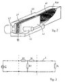
- FIG. 1 shows a longitudinal section and FIG. 2 shows a perspective illustration of a tunable adaptation network which is coupled to a microwave line L.
- the microwave line L is a coaxial line with the inner conductor LI.
- the microwave line L is fed at one input by a generator G and is terminated at its opposite output with a changing load resistor ZL.
- the T equivalent circuit diagram with the impedances Z1 and Z2 inserted into the microwave line L stands for the matching network, which serves to transform the respective load resistance ZL to the line impedance.
- the matching network has a first line L1 and a second line L2, each of which has one end in contact with the interrupted inner conductor LI of the coaxial microwave line L.
- the two lines L1 and L2 are connected to one another at the opposite end.
- a third line L3 branches off from this connection point.
- the lines L1, L2 and L3 are designed as strip lines.
- the outer conductor to the strip conductors L1, L2 and L3 is formed by the housing GS indicated by hatching, which is connected to the outer conductor of the coaxial microwave line L.
- the plate-shaped inner conductors of the two strip lines L1 and L2 are covered with ferrite layers F1 and F2 on the adjacent sides.
- the plate-shaped inner conductor is covered on both sides with ferrite layers F31 and F32.
- the outer conductor GS of the three lines can also be coated with ferrite.
- the same also applies if the lines L1, L2 and L3 are realized as coaxial lines.
- the arrows drawn in FIG. 1 outside the matching network indicate that the two lines L1 and L2 are exposed to a magnetic field M1 and separately the third line L3 is exposed to a magnetic field M2.
- the magnetic fields M1 and M2 can be changed independently of one another.
- the electrical length of these two lines L1 and L2 can be varied. Irrespective of this, the electrical length of the third line L3 can be varied by means of the changeable magnetic field M2 which acts on the ferrites F31 and F32.
- the described arrangement of the lines L1, L2 and L3 actually represents two different line systems.
- the one line system consisting of the first line L1 and the second line L2, together with the housing GS form a shielded two-wire line on which two wave modes exist Common mode and a push mode.
- Push-pull mode is when the currents flowing on lines L1 and L2 are equal and opposite directions
- common mode is when the currents flowing on lines L1 and L2 are equal and equally directed.
- the second line system consisting of line L3 and housing GS, only the common mode can be propagated.
- the ferrite material on lines L1 and L2 is arranged between the lines (see FIG. 1) and is therefore only effective for push-pull mode.
- the push-pull impedance Zg of the lines L1, L2 is matched by the magnetic field M1 and the common-mode impedance Zs of the line L3 by the magnetic field M2.
- the impedances Z1 and Z2 specified in the equivalent circuit diagram (see FIG. 3) of the matching network then have the following relationship to the common-mode impedance Z s and the push-pull impedance Z g :
- Z1 Z G
- Z2 Z. s - Z G 2nd
- the heat loss generated in the ferrites F1, F2, F31 and F32 can be very effective and simple with the help of cooling channels which run through the inner conductor and / or the outer conductor of the lines L1, L2 and L3 designed as strip lines or as coaxial lines.
- a cooling channel designated by K is indicated in FIG.
- the changeable magnetic fields M1 and M2 are generated by controllable electromagnets.
- permanent magnets can also be provided, which generate a static magnetic field of such strength that the ferrites are operated above their gyromagnetic resonance, where they have the lowest losses.
- the use of permanent magnets and electromagnets has the advantage that only small currents are required to tune the ferrite-loaded lines, since thanks to the permanent magnets only part of the required Magnetization must be applied by the electromagnet. It is also advantageous that if the control current for the electromagnets fails, the power loss in the ferrites does not increase very much because the permanent magnets always keep the magnetization of the ferrites above the gyromagnetic resonance.
Landscapes
- Variable-Direction Aerials And Aerial Arrays (AREA)
- Non-Reversible Transmitting Devices (AREA)
- Plasma Technology (AREA)
Abstract
Description
- Die vorliegende Erfindung betrifft ein abstimmbares Anpassungsnetzwerk, das an eine Mikrowellenleitung ankoppelbar ist.
- Wie aus einem Vortrag von F. Durodie, New Antenna Impedance Evaluation and Matching Tools for TEXTOR's ICRH System, auf dem 16th Symposium on Fusion Technology (SOFT), London, 3 - 7 Sept. 1990 hervorgeht, wird ein abstimmbares Anpassungsnetzwerk z.B. für eine Mikrowellenleitung benötigt, die in die Plasma-Brennkammer eines Fusionsreaktors Mikrowellenenergie hoher Leistung einkoppelt. Da die Plasma-Brennkammer einen ständig sich ändernden Lastwiderstand für die Mikrowellenleitung darstellt und damit der die Mikrowellenenergie erzeugende Generator nicht durch aufgrund von Fehlanpassung entstehenden Reflexionen beschädigt wird, ist der jeweils auftretende Lastwiderstand auf den Leitungswellenwiderstand zu transformieren. Gemäß der genannten Veröffentlichung werden zu diesem Zweck zwei durch eine exakt zu bemessende Transformationsleitungslänge voneinander getrennte, abstimmbare Kapazitäten an die Mikrowellenleitung angekoppelt. Die Abstimmung der Kapazitäten erfolgt durch eine mechanisch aufwendige pneumatische Vorrichtung. Da sich der Lastwiderstand aber sehr schnell ändern kann, dürfte diese Anordnung zu träge sein, um eine möglichst verzögerungsarme Anpassung bewerkstelligen zu können.
- Nicht nur für den geschilderten Einsatzfall, sondern immer dann, wenn an eine Mikrowellenleitung ein sich ändernder Lastwiderstand angeschaltet ist, kann ein abstimmbares Anpassungsnetzwerk verwendet werden.
- Der Erfindung liegt die Aufgabe zugrunde, ein Anpassungsnetzwerk anzugeben, das mit geringem Aufwand schnell auf eine gewünschte Impedanz abgestimmt werden kann.
- Erfindungsgemäß wird diese Aufgabe durch die Merkmale des Patentanspruchs 1 gelöst. Vorteilhafte Ausführungen der Erfindung gehen aus den Unteransprüchen hervor.
- Dadurch, daß das Anpassungsnetzwerk elektrisch, ohne mechanisch bewegbare Teile abgestimmt werden kann, ist eine verzögerungsarme Impedanzanpassung bei sich rasch änderndem Lastwiderstand einer Mikrowellenleitung gewährleistet.
- Ein weiterer Vorteil der Anordnung ist, daß zwischen den beiden variablen Reaktanzen des im Eingang genannten Anpassungsnetzwerkes keine Transformationsleitung erforderlich ist.
- Anhand eines in der Zeichnung dargestellten Ausführungsbeispiels wird nachfolgend die Erfindung näher erläutert.
Es zeigen: - Figur 1 ein Anpassungsnetzwerk im Längsschnitt und
- Figur 2 eine perspektivische Darstellung dessen,
- Figur 3 ein Ersatzschaltbild dieses Anpassungsnetzwerks.
- Der Figur 1 ist ein Längsschnitt und der Figur 2 eine perspektivische Darstellung eines abstimmbaren Anpassungsnetzwerkes zu entnehmen, das an eine Mikrowellenleitung L angekoppelt ist. In dem gezeigten Ausführungsbeispiel ist die Mikrowellenleitung L eine Koaxialleitung mit dem Innenleiter LI. Wie bereits einleitend dargelegt und durch das Ersatzschaltbild in Figur 3 verdeutlicht, wird die Mikrowellenleitung L an einem Eingang von einem Generator G gespeist und ist an seinem gegenüberliegenden Ausgang mit einem sich ändernden Lastwiderstand ZL abgeschlossen. Das in die Mikrowellenleitung L eingefügte T-Ersatzschaltbild mit den Impedanzen Z1 und Z2 steht für das Anpassungsnetzwerk, welches dazu dient, den jeweiligen Lastwiderstand ZL auf den Leitungswellenwiderstand zu transformieren.
- Das Anpassungsnetzwerk besitzt eine erste Leitung L1 und eine zweite Leitung L2, von denen jede mit einem Ende mit dem unterbrochenen Innenleiter LI der koaxialen Mikrowellenleitung L kontaktiert ist. Am gegenüberliegenden Ende sind die beiden Leitungen L1 und L2 miteinander verbunden. Von diesem Verbindungspunkt zweigt eine dritte Leitung L3 ab. Bei dem in den Figuren 1 und 2 dargestellten Ausführungsbeispiel sind die Leitungen L1, L2 und L3 als Streifenleiter ausgeführt. Den Außenleiter zu den Streifenleitern L1, L2 und L3 bildet das durch Schraffur angedeutete Gehäuse GS, das mit dem Außenleiter der koaxiaien Mikrowellenleitung L verbunden ist. Bei der dargestellten Ausführung sind die plattenförmigen Innenleiter der beiden Streifenleitungen L1 und L2 auf den einander benachbarten Seiten mit Ferritschichten F1 und F2 belegt. Bei der dritten Leitung L3 ist der plattenförmige Innenleiter beidseitig mit Ferritschichten F31 und F32 belegt. Anstatt die Ferritschichten Fl, F2, F31, F32 auf den Innenleitern anzubringen, kann auch der Außenleiter GS der drei Leitungen mit Ferrit beschichtet werden. Das gleiche gilt auch, wenn die Leitungen L1, L2 und L3 als Koaxialleitungen realisiert sind. Die in Figur 1 eingezeichneten Pfeile außerhalb des Anpassungsnetzwerkes deuten an, daß die beiden Leitungen L1 und L2 einem Magnetfeld M1 und getrennt davon die dritte Leitung L3 einem Magnetfeld M2 ausgesetzt ist. Es handelt sich um unabhängig voneinander veränderbare Magnetfelder M1 und M2. Mit dem auf die ferritbelasteten Leitungen L1 und L2 einwirkenden Magnetfeld M1 läßt sich die elektrische Länge dieser beiden Leitungen L1 und L2 variieren. Unabhängig davon läßt sich die elektrische Länge der dritten Leitung L3 durch das veränderbare,auf die Ferrite F31 und F32 einwirkende Magnetfeld M2 variieren.
- Die beschriebene Anordnung der Leitungen L1, L2 und L3 stellt eigentlich zwei verschiedene Leitungssysteme dar. Das eine Leitungssystem, bestehend aus der ersten Leitung L1 und der zweiten Leitung L2, bilden zusammen mit dem Gehäuse GS eine geschirmte Zweidrahtleitung, auf der zwei Wellenmoden existieren, ein Gleichtaktmode und ein Gegentaktmode. Gegentaktmode liegt vor, wenn die in den Leitungen L1 und L2 fließenden Ströme gleich groß und entgegengesetzt gerichtet sind, und Gleichtaktmode liegt vor, wenn die in den Leitungen L1 und L2 fließenden Ströme gleich groß und gleich gerichtet sind.
Im zweiten Leitungssystem, bestehend aus der Leitung L3 und dem Gehäuse GS, ist nur der Gleichtaktmode ausbreitungsfähig. Das Ferritmaterial auf den Leitungen L1 und L2 ist zwischen den Leitungen angeordnet (s. Fig. 1) und somit nur für den Gegentaktmode wirksam. Durch das Magnetfeld M1 wird die Gegentaktimpedanz Zg der Leitungen L1, L2 abgestimmt und durch das Magnetfeld M2 die Gleichtaktimpedanz Zs der Leitung L3. - Die im Ersatzschaltbild (siehe Figur 3) des Anpassungsnetzwerkes angegebenen Impedanzen Z1 und Z2 haben dann folgende Beziehung zur Gleichtaktimpedanz Zs und zur Gegentaktimpedanz Zg:


- Für den Fall, daß das Anpassungsnetzwerk mit sehr hohen Leistungen betrieben wird, ist es zweckmäßig die Leitungen L1, L2 und L3 zu kühlen. Die in den Ferriten F1, F2, F31 und F32 entstehende Verlustwärme kann sehr wirkungsvoll und auf einfache Weise mit Hilfe von Kühlkanälen, welche den Innenleiter und/oder den Außenleiter der als Streifenleitungen oder als Koaxialleitungen ausgeführten Leitungen L1, L2 und L3 durchziehen. In der Figur 1 ist ein mit K bezeichneter Kühlkanal angedeutet.
- Die veränderbaren Magnetfelder M1 und M2 werden von steuerbaren Elektromagneten erzeugt. Es können aber auch zusätzlich Permanentmagneten vorgesehen werden, die ein statisches Magnetfeld von solcher Stärke erzeugen, daß die Ferrite oberhalb ihrer gyromagnetischen Resonanz betrieben werden, wo sie die geringsten Verluste aufweisen. Die Verwendung von Permanentmagneten und Elektromagneten bringt den Vorteil, daß zur Abstimmung der ferritbelasteten Leitungen nur kleine Ströme erforderlich sind, da dank der Permanentmagneten nur ein Teil der erforderlichen Magnetisierung von den Elektromagneten aufgebracht werden muß. Vorteilhaft ist auch, daß bei einem evtl. Ausfall des Steuerstroms für die Elektromagneten die Verlustleistung in den Ferriten nicht sehr stark ansteigt, weil die Permanentmagneten die Magnetisierung der Ferrite immer oberhalb der gyromagnetischen Resonanz halten.
Claims (3)
- Abstimmbares Anpassungsnetzwerk, das an eine Mikrowellenleitung ankoppelbar ist, dadurch gekennzeichnet,
daß es eine erste und eine zweite Leitung (L1, L2), die beide an einem Ende miteinander verbunden sind und deren jeweils anderes Ende für die Ankopplung an die Mikrowellenleitung (L) dient, und eine dritte Leitung (3) aufweist, die vom Verbindungspunkt der beiden anderen Leitungen (L1, L2) abzweigt, daß die erste und/oder die zweite Leitung (L1, L2) und die dritte Leitung (L3) mit Ferrit (F1, F2, F31, F32) belastet sind und daß das Ferrit (F1, F2) der ersten und/oder zweiten Leitung (L1, L2) und das Ferrit (F31, F32) der dritten Leitung (L3) separaten unabhängig voneinander veränderbaren Magnetfeldern (Ml, M2) ausgesetzt sind. - Abstimmbares Anpassungsnetzwerk nach Anspruch 1, dadurch gekennzeichnet,
daß die drei Leitungen (L1, L2, L3) Koaxialleiter sind, deren Innenleiter und/oder Außenleiter zumindest teilweise mit Ferrit beschichtet sind. - Abstimmbares Anpassungsnetzwerk nach Anspruch 1, dadurch gekennzeichnet,
daß die drei Leitungen (L1, L2, L3) Streifenleiter sind, deren Innenleiter und/oder Außenleiter zumindest teilweise mit Ferrit (F1, F2, F31, F32) beschichtet sind.
Applications Claiming Priority (3)
| Application Number | Priority Date | Filing Date | Title |
|---|---|---|---|
| DE4122290 | 1991-07-05 | ||
| DE4122290A DE4122290C1 (de) | 1991-07-05 | 1991-07-05 | |
| PCT/DE1992/000420 WO1993001627A1 (de) | 1991-07-05 | 1992-05-23 | Abstimmbares anpassungsnetzwerk |
Publications (2)
| Publication Number | Publication Date |
|---|---|
| EP0593500A1 EP0593500A1 (de) | 1994-04-27 |
| EP0593500B1 true EP0593500B1 (de) | 1996-08-21 |
Family
ID=6435506
Family Applications (1)
| Application Number | Title | Priority Date | Filing Date |
|---|---|---|---|
| EP92910707A Expired - Lifetime EP0593500B1 (de) | 1991-07-05 | 1992-05-23 | Abstimmbares anpassungsnetzwerk |
Country Status (6)
| Country | Link |
|---|---|
| US (1) | US5430417A (de) |
| EP (1) | EP0593500B1 (de) |
| JP (1) | JPH07500225A (de) |
| CA (1) | CA2112819A1 (de) |
| DE (1) | DE4122290C1 (de) |
| WO (1) | WO1993001627A1 (de) |
Families Citing this family (40)
| Publication number | Priority date | Publication date | Assignee | Title |
|---|---|---|---|---|
| FI96550C (fi) * | 1994-06-30 | 1996-07-10 | Nokia Telecommunications Oy | Summausverkko |
| DE19532780A1 (de) * | 1995-09-06 | 1997-03-13 | Pates Tech Patentverwertung | Dielektrischer Wellenleiter |
| USRE45667E1 (en) * | 2000-06-13 | 2015-09-08 | Christos Tsironis | Adaptable pre-matched tuner system and method |
| EP1301960A1 (de) * | 2000-07-20 | 2003-04-16 | Paratek Microwave, Inc. | Abstimmbare mikrowellenanordnungen mit selbsteinstellender anpassungsschaltung |
| US7865154B2 (en) * | 2000-07-20 | 2011-01-04 | Paratek Microwave, Inc. | Tunable microwave devices with auto-adjusting matching circuit |
| US8064188B2 (en) | 2000-07-20 | 2011-11-22 | Paratek Microwave, Inc. | Optimized thin film capacitors |
| US8744384B2 (en) | 2000-07-20 | 2014-06-03 | Blackberry Limited | Tunable microwave devices with auto-adjusting matching circuit |
| US7075385B2 (en) * | 2004-04-29 | 2006-07-11 | Kathrein-Werke Kg | Impedance converter device |
| US9406444B2 (en) | 2005-11-14 | 2016-08-02 | Blackberry Limited | Thin film capacitors |
| US8125399B2 (en) | 2006-01-14 | 2012-02-28 | Paratek Microwave, Inc. | Adaptively tunable antennas incorporating an external probe to monitor radiated power |
| US7711337B2 (en) * | 2006-01-14 | 2010-05-04 | Paratek Microwave, Inc. | Adaptive impedance matching module (AIMM) control architectures |
| US8325097B2 (en) | 2006-01-14 | 2012-12-04 | Research In Motion Rf, Inc. | Adaptively tunable antennas and method of operation therefore |
| US8299867B2 (en) | 2006-11-08 | 2012-10-30 | Research In Motion Rf, Inc. | Adaptive impedance matching module |
| US7535312B2 (en) * | 2006-11-08 | 2009-05-19 | Paratek Microwave, Inc. | Adaptive impedance matching apparatus, system and method with improved dynamic range |
| US7714676B2 (en) | 2006-11-08 | 2010-05-11 | Paratek Microwave, Inc. | Adaptive impedance matching apparatus, system and method |
| US7917104B2 (en) | 2007-04-23 | 2011-03-29 | Paratek Microwave, Inc. | Techniques for improved adaptive impedance matching |
| US8213886B2 (en) | 2007-05-07 | 2012-07-03 | Paratek Microwave, Inc. | Hybrid techniques for antenna retuning utilizing transmit and receive power information |
| US7991363B2 (en) | 2007-11-14 | 2011-08-02 | Paratek Microwave, Inc. | Tuning matching circuits for transmitter and receiver bands as a function of transmitter metrics |
| US8072285B2 (en) | 2008-09-24 | 2011-12-06 | Paratek Microwave, Inc. | Methods for tuning an adaptive impedance matching network with a look-up table |
| US8067858B2 (en) * | 2008-10-14 | 2011-11-29 | Paratek Microwave, Inc. | Low-distortion voltage variable capacitor assemblies |
| US8472888B2 (en) | 2009-08-25 | 2013-06-25 | Research In Motion Rf, Inc. | Method and apparatus for calibrating a communication device |
| US9026062B2 (en) | 2009-10-10 | 2015-05-05 | Blackberry Limited | Method and apparatus for managing operations of a communication device |
| US8803631B2 (en) | 2010-03-22 | 2014-08-12 | Blackberry Limited | Method and apparatus for adapting a variable impedance network |
| US8289043B2 (en) * | 2010-03-26 | 2012-10-16 | International Business Machines Corporation | Simulation of printed circuit board impedance variations and crosstalk effects |
| CA2797074C (en) | 2010-04-20 | 2018-08-14 | Research In Motion Rf, Inc. | Method and apparatus for managing interference in a communication device |
| US9379454B2 (en) | 2010-11-08 | 2016-06-28 | Blackberry Limited | Method and apparatus for tuning antennas in a communication device |
| US8712340B2 (en) | 2011-02-18 | 2014-04-29 | Blackberry Limited | Method and apparatus for radio antenna frequency tuning |
| US8655286B2 (en) | 2011-02-25 | 2014-02-18 | Blackberry Limited | Method and apparatus for tuning a communication device |
| US8594584B2 (en) | 2011-05-16 | 2013-11-26 | Blackberry Limited | Method and apparatus for tuning a communication device |
| US8626083B2 (en) | 2011-05-16 | 2014-01-07 | Blackberry Limited | Method and apparatus for tuning a communication device |
| WO2013022826A1 (en) | 2011-08-05 | 2013-02-14 | Research In Motion Rf, Inc. | Method and apparatus for band tuning in a communication device |
| US8948889B2 (en) | 2012-06-01 | 2015-02-03 | Blackberry Limited | Methods and apparatus for tuning circuit components of a communication device |
| US9853363B2 (en) | 2012-07-06 | 2017-12-26 | Blackberry Limited | Methods and apparatus to control mutual coupling between antennas |
| US9246223B2 (en) | 2012-07-17 | 2016-01-26 | Blackberry Limited | Antenna tuning for multiband operation |
| US9413066B2 (en) | 2012-07-19 | 2016-08-09 | Blackberry Limited | Method and apparatus for beam forming and antenna tuning in a communication device |
| US9350405B2 (en) | 2012-07-19 | 2016-05-24 | Blackberry Limited | Method and apparatus for antenna tuning and power consumption management in a communication device |
| US9362891B2 (en) | 2012-07-26 | 2016-06-07 | Blackberry Limited | Methods and apparatus for tuning a communication device |
| US10404295B2 (en) | 2012-12-21 | 2019-09-03 | Blackberry Limited | Method and apparatus for adjusting the timing of radio antenna tuning |
| US9374113B2 (en) | 2012-12-21 | 2016-06-21 | Blackberry Limited | Method and apparatus for adjusting the timing of radio antenna tuning |
| US9438319B2 (en) | 2014-12-16 | 2016-09-06 | Blackberry Limited | Method and apparatus for antenna selection |
Family Cites Families (8)
| Publication number | Priority date | Publication date | Assignee | Title |
|---|---|---|---|---|
| BE474967A (de) * | 1944-11-16 | |||
| US3384841A (en) * | 1966-03-10 | 1968-05-21 | Bell Telephone Labor Inc | Ferrite phase shifter having longitudinal and circular magnetic fields applied to the ferrite |
| FR2050584A5 (de) * | 1969-06-18 | 1971-04-02 | Lignes Telegraph Telephon | |
| US3745488A (en) * | 1971-02-16 | 1973-07-10 | Gte Automatic Electric Lab Inc | Microwave impedance-matching network |
| US3792385A (en) * | 1972-11-06 | 1974-02-12 | Rca Corp | Coaxial magnetic slug tuner |
| JPS5596701A (en) * | 1979-01-19 | 1980-07-23 | Nippon Telegr & Teleph Corp <Ntt> | Coaxial variable attenuator |
| US4754229A (en) * | 1986-01-08 | 1988-06-28 | Kabushiki Kaisha Toshiba | Matching circuit for a microwave device |
| US5065118A (en) * | 1990-07-26 | 1991-11-12 | Applied Materials, Inc. | Electronically tuned VHF/UHF matching network |
-
1991
- 1991-07-05 DE DE4122290A patent/DE4122290C1/de not_active Expired - Fee Related
-
1992
- 1992-05-23 JP JP4509754A patent/JPH07500225A/ja active Pending
- 1992-05-23 CA CA002112819A patent/CA2112819A1/en not_active Abandoned
- 1992-05-23 US US08/182,209 patent/US5430417A/en not_active Expired - Fee Related
- 1992-05-23 WO PCT/DE1992/000420 patent/WO1993001627A1/de not_active Ceased
- 1992-05-23 EP EP92910707A patent/EP0593500B1/de not_active Expired - Lifetime
Non-Patent Citations (1)
| Title |
|---|
| IRE TRANSACTIONS ON MICROWAVE THEORY AND TECHNIQUES. Bd. 7, Nr. 2, April 1959,NEW YORK US Seiten 296-297, C.E. MUEHE: 'Quarter-wave compensation of resonant discontinuities' siehe Seite 296, mittlere Spalte, Zeile 21 - Zeile 30 siehe Seite 297, linke Spalte, Zeile 1 - Zeile 4; Abbildung 1 * |
Also Published As
| Publication number | Publication date |
|---|---|
| DE4122290C1 (de) | 1992-11-19 |
| CA2112819A1 (en) | 1993-01-21 |
| JPH07500225A (ja) | 1995-01-05 |
| WO1993001627A1 (de) | 1993-01-21 |
| EP0593500A1 (de) | 1994-04-27 |
| US5430417A (en) | 1995-07-04 |
Similar Documents
| Publication | Publication Date | Title |
|---|---|---|
| DE4122290C1 (de) | ||
| DE2122337C2 (de) | Hohlraumresonator-Filter | |
| DE3037930A1 (de) | Reziproker leistungsteiler | |
| DE3685553T2 (de) | Pin-dioden-daempfungsglieder. | |
| DE2643094A1 (de) | Verallgemeinertes wellenleiter- bandpassfilter | |
| DE3111106C2 (de) | ||
| DE1909092A1 (de) | Hybridkoppler mit 90 deg.-Phasenverschiebung | |
| DE68917373T2 (de) | Magnetisch abstimmbares Bandpassfilter. | |
| DE2746376C2 (de) | Koppelvorrichtung zwischen einer Koaxialleitung und einem Hohlleiter | |
| DE927099C (de) | Verstaerker mit negativem Widerstand | |
| DE1441627B2 (de) | Anordnung zur uebertragung elektrischer wellen mit frequenz abhaengiger daempfung | |
| DE2521956C3 (de) | Polarisationsweiche | |
| EP0978894B1 (de) | Breitbandiger koaxialer Überspannungsableiter | |
| EP2137788A1 (de) | Wellenleiter-system mit differenziellem wellenleiter | |
| DE2828047B1 (de) | Frequenzabhaengiges Koppelsystem | |
| DE3122084C2 (de) | ||
| EP0124168B1 (de) | Mischer | |
| DE3324540C2 (de) | Breitbandiger Mikrowellenverstärker | |
| EP0101612B1 (de) | Oszillator mit einem Zweipol als aktivem Element | |
| DE2815668A1 (de) | Breitband-isolator | |
| DE4411894C1 (de) | Leistungs-Impedanz-Transformator für Transistor-Gegentakt-Leistungsverstärker | |
| DE4136110C1 (en) | Transition piece between waveguide and microstrip conductor - has substrate in housing with short circuiting wall in region of bridging piece leading from fin conductor to microstrip | |
| DE102015107729A1 (de) | Combiner-Anordnung | |
| DE3006387A1 (de) | Anpassnetzwerk fuer einen mikrowellen-verzweigungszirkulator oder eine mikrowellen-einweg-verzweigungsleitung | |
| EP0109680B1 (de) | Als Bode-Entzerrer ausgebildeter einstellbarer Dämpfungentzerrer |
Legal Events
| Date | Code | Title | Description |
|---|---|---|---|
| PUAI | Public reference made under article 153(3) epc to a published international application that has entered the european phase |
Free format text: ORIGINAL CODE: 0009012 |
|
| 17P | Request for examination filed |
Effective date: 19931208 |
|
| AK | Designated contracting states |
Kind code of ref document: A1 Designated state(s): CH FR GB LI |
|
| RAP1 | Party data changed (applicant data changed or rights of an application transferred) |
Owner name: AFT ADVANCED FERRITE TECHNOLOGY GMBH |
|
| 17Q | First examination report despatched |
Effective date: 19950926 |
|
| GRAH | Despatch of communication of intention to grant a patent |
Free format text: ORIGINAL CODE: EPIDOS IGRA |
|
| GRAA | (expected) grant |
Free format text: ORIGINAL CODE: 0009210 |
|
| AK | Designated contracting states |
Kind code of ref document: B1 Designated state(s): CH FR GB LI |
|
| REG | Reference to a national code |
Ref country code: CH Ref legal event code: NV Representative=s name: KIRKER & CIE SA |
|
| GBT | Gb: translation of ep patent filed (gb section 77(6)(a)/1977) |
Effective date: 19960821 |
|
| ET | Fr: translation filed |
Free format text: CORRECTIONS |
|
| PLBE | No opposition filed within time limit |
Free format text: ORIGINAL CODE: 0009261 |
|
| STAA | Information on the status of an ep patent application or granted ep patent |
Free format text: STATUS: NO OPPOSITION FILED WITHIN TIME LIMIT |
|
| 26N | No opposition filed | ||
| PGFP | Annual fee paid to national office [announced via postgrant information from national office to epo] |
Ref country code: FR Payment date: 19980318 Year of fee payment: 7 |
|
| PGFP | Annual fee paid to national office [announced via postgrant information from national office to epo] |
Ref country code: GB Payment date: 19980522 Year of fee payment: 7 |
|
| PGFP | Annual fee paid to national office [announced via postgrant information from national office to epo] |
Ref country code: CH Payment date: 19980819 Year of fee payment: 7 |
|
| PG25 | Lapsed in a contracting state [announced via postgrant information from national office to epo] |
Ref country code: GB Free format text: LAPSE BECAUSE OF NON-PAYMENT OF DUE FEES Effective date: 19990523 |
|
| PG25 | Lapsed in a contracting state [announced via postgrant information from national office to epo] |
Ref country code: LI Free format text: LAPSE BECAUSE OF NON-PAYMENT OF DUE FEES Effective date: 19990531 Ref country code: CH Free format text: LAPSE BECAUSE OF NON-PAYMENT OF DUE FEES Effective date: 19990531 |
|
| REG | Reference to a national code |
Ref country code: CH Ref legal event code: PL |
|
| GBPC | Gb: european patent ceased through non-payment of renewal fee |
Effective date: 19990523 |
|
| PG25 | Lapsed in a contracting state [announced via postgrant information from national office to epo] |
Ref country code: FR Free format text: LAPSE BECAUSE OF NON-PAYMENT OF DUE FEES Effective date: 20000131 |
|
| REG | Reference to a national code |
Ref country code: FR Ref legal event code: ST |