EP0590336B1 - Optoelectronic element with narrow beam angle - Google Patents
Optoelectronic element with narrow beam angle Download PDFInfo
- Publication number
- EP0590336B1 EP0590336B1 EP93114017A EP93114017A EP0590336B1 EP 0590336 B1 EP0590336 B1 EP 0590336B1 EP 93114017 A EP93114017 A EP 93114017A EP 93114017 A EP93114017 A EP 93114017A EP 0590336 B1 EP0590336 B1 EP 0590336B1
- Authority
- EP
- European Patent Office
- Prior art keywords
- reflector
- carrier strip
- semiconductor chip
- optoelectronic component
- opto
- Prior art date
- Legal status (The legal status is an assumption and is not a legal conclusion. Google has not performed a legal analysis and makes no representation as to the accuracy of the status listed.)
- Expired - Lifetime
Links
- 230000005693 optoelectronics Effects 0.000 title claims description 18
- 239000004065 semiconductor Substances 0.000 claims description 26
- 238000000034 method Methods 0.000 claims description 8
- 229920003023 plastic Polymers 0.000 claims description 7
- 230000005855 radiation Effects 0.000 claims description 7
- 238000004519 manufacturing process Methods 0.000 claims description 6
- 239000004033 plastic Substances 0.000 claims description 6
- 239000000463 material Substances 0.000 claims description 2
- 238000001465 metallisation Methods 0.000 claims 2
- 238000010276 construction Methods 0.000 claims 1
- 239000002184 metal Substances 0.000 claims 1
- 239000010410 layer Substances 0.000 description 4
- 150000001875 compounds Chemical class 0.000 description 3
- 238000002161 passivation Methods 0.000 description 3
- 238000005266 casting Methods 0.000 description 2
- 230000000875 corresponding effect Effects 0.000 description 2
- 230000008878 coupling Effects 0.000 description 2
- 238000010168 coupling process Methods 0.000 description 2
- 238000005859 coupling reaction Methods 0.000 description 2
- 230000007774 longterm Effects 0.000 description 2
- 238000004382 potting Methods 0.000 description 2
- 229920003002 synthetic resin Polymers 0.000 description 2
- 239000000057 synthetic resin Substances 0.000 description 2
- 239000000853 adhesive Substances 0.000 description 1
- 238000004026 adhesive bonding Methods 0.000 description 1
- 230000001070 adhesive effect Effects 0.000 description 1
- 238000013459 approach Methods 0.000 description 1
- 230000008901 benefit Effects 0.000 description 1
- 230000008859 change Effects 0.000 description 1
- 230000007423 decrease Effects 0.000 description 1
- 230000000694 effects Effects 0.000 description 1
- 230000005684 electric field Effects 0.000 description 1
- 230000006872 improvement Effects 0.000 description 1
- 238000005259 measurement Methods 0.000 description 1
- 230000009467 reduction Effects 0.000 description 1
- 239000002210 silicon-based material Substances 0.000 description 1
- 239000002356 single layer Substances 0.000 description 1
- 238000005476 soldering Methods 0.000 description 1
Images


Classifications
-
- H—ELECTRICITY
- H01—ELECTRIC ELEMENTS
- H01L—SEMICONDUCTOR DEVICES NOT COVERED BY CLASS H10
- H01L33/00—Semiconductor devices having potential barriers specially adapted for light emission; Processes or apparatus specially adapted for the manufacture or treatment thereof or of parts thereof; Details thereof
- H01L33/48—Semiconductor devices having potential barriers specially adapted for light emission; Processes or apparatus specially adapted for the manufacture or treatment thereof or of parts thereof; Details thereof characterised by the semiconductor body packages
- H01L33/62—Arrangements for conducting electric current to or from the semiconductor body, e.g. lead-frames, wire-bonds or solder balls
-
- H—ELECTRICITY
- H01—ELECTRIC ELEMENTS
- H01L—SEMICONDUCTOR DEVICES NOT COVERED BY CLASS H10
- H01L31/00—Semiconductor devices sensitive to infrared radiation, light, electromagnetic radiation of shorter wavelength or corpuscular radiation and specially adapted either for the conversion of the energy of such radiation into electrical energy or for the control of electrical energy by such radiation; Processes or apparatus specially adapted for the manufacture or treatment thereof or of parts thereof; Details thereof
- H01L31/02—Details
- H01L31/0232—Optical elements or arrangements associated with the device
- H01L31/02327—Optical elements or arrangements associated with the device the optical elements being integrated or being directly associated to the device, e.g. back reflectors
-
- H—ELECTRICITY
- H01—ELECTRIC ELEMENTS
- H01L—SEMICONDUCTOR DEVICES NOT COVERED BY CLASS H10
- H01L31/00—Semiconductor devices sensitive to infrared radiation, light, electromagnetic radiation of shorter wavelength or corpuscular radiation and specially adapted either for the conversion of the energy of such radiation into electrical energy or for the control of electrical energy by such radiation; Processes or apparatus specially adapted for the manufacture or treatment thereof or of parts thereof; Details thereof
- H01L31/12—Semiconductor devices sensitive to infrared radiation, light, electromagnetic radiation of shorter wavelength or corpuscular radiation and specially adapted either for the conversion of the energy of such radiation into electrical energy or for the control of electrical energy by such radiation; Processes or apparatus specially adapted for the manufacture or treatment thereof or of parts thereof; Details thereof structurally associated with, e.g. formed in or on a common substrate with, one or more electric light sources, e.g. electroluminescent light sources, and electrically or optically coupled thereto
- H01L31/16—Semiconductor devices sensitive to infrared radiation, light, electromagnetic radiation of shorter wavelength or corpuscular radiation and specially adapted either for the conversion of the energy of such radiation into electrical energy or for the control of electrical energy by such radiation; Processes or apparatus specially adapted for the manufacture or treatment thereof or of parts thereof; Details thereof structurally associated with, e.g. formed in or on a common substrate with, one or more electric light sources, e.g. electroluminescent light sources, and electrically or optically coupled thereto the semiconductor device sensitive to radiation being controlled by the light source or sources
- H01L31/167—Semiconductor devices sensitive to infrared radiation, light, electromagnetic radiation of shorter wavelength or corpuscular radiation and specially adapted either for the conversion of the energy of such radiation into electrical energy or for the control of electrical energy by such radiation; Processes or apparatus specially adapted for the manufacture or treatment thereof or of parts thereof; Details thereof structurally associated with, e.g. formed in or on a common substrate with, one or more electric light sources, e.g. electroluminescent light sources, and electrically or optically coupled thereto the semiconductor device sensitive to radiation being controlled by the light source or sources the light sources and the devices sensitive to radiation all being semiconductor devices characterised by potential barriers
-
- H—ELECTRICITY
- H01—ELECTRIC ELEMENTS
- H01L—SEMICONDUCTOR DEVICES NOT COVERED BY CLASS H10
- H01L33/00—Semiconductor devices having potential barriers specially adapted for light emission; Processes or apparatus specially adapted for the manufacture or treatment thereof or of parts thereof; Details thereof
- H01L33/48—Semiconductor devices having potential barriers specially adapted for light emission; Processes or apparatus specially adapted for the manufacture or treatment thereof or of parts thereof; Details thereof characterised by the semiconductor body packages
- H01L33/58—Optical field-shaping elements
- H01L33/60—Reflective elements
-
- H—ELECTRICITY
- H01—ELECTRIC ELEMENTS
- H01L—SEMICONDUCTOR DEVICES NOT COVERED BY CLASS H10
- H01L2224/00—Indexing scheme for arrangements for connecting or disconnecting semiconductor or solid-state bodies and methods related thereto as covered by H01L24/00
- H01L2224/01—Means for bonding being attached to, or being formed on, the surface to be connected, e.g. chip-to-package, die-attach, "first-level" interconnects; Manufacturing methods related thereto
- H01L2224/42—Wire connectors; Manufacturing methods related thereto
- H01L2224/47—Structure, shape, material or disposition of the wire connectors after the connecting process
- H01L2224/48—Structure, shape, material or disposition of the wire connectors after the connecting process of an individual wire connector
- H01L2224/4805—Shape
- H01L2224/4809—Loop shape
- H01L2224/48091—Arched
-
- H—ELECTRICITY
- H01—ELECTRIC ELEMENTS
- H01L—SEMICONDUCTOR DEVICES NOT COVERED BY CLASS H10
- H01L2224/00—Indexing scheme for arrangements for connecting or disconnecting semiconductor or solid-state bodies and methods related thereto as covered by H01L24/00
- H01L2224/01—Means for bonding being attached to, or being formed on, the surface to be connected, e.g. chip-to-package, die-attach, "first-level" interconnects; Manufacturing methods related thereto
- H01L2224/42—Wire connectors; Manufacturing methods related thereto
- H01L2224/47—Structure, shape, material or disposition of the wire connectors after the connecting process
- H01L2224/48—Structure, shape, material or disposition of the wire connectors after the connecting process of an individual wire connector
- H01L2224/481—Disposition
- H01L2224/48151—Connecting between a semiconductor or solid-state body and an item not being a semiconductor or solid-state body, e.g. chip-to-substrate, chip-to-passive
- H01L2224/48221—Connecting between a semiconductor or solid-state body and an item not being a semiconductor or solid-state body, e.g. chip-to-substrate, chip-to-passive the body and the item being stacked
- H01L2224/48245—Connecting between a semiconductor or solid-state body and an item not being a semiconductor or solid-state body, e.g. chip-to-substrate, chip-to-passive the body and the item being stacked the item being metallic
- H01L2224/48247—Connecting between a semiconductor or solid-state body and an item not being a semiconductor or solid-state body, e.g. chip-to-substrate, chip-to-passive the body and the item being stacked the item being metallic connecting the wire to a bond pad of the item
-
- H—ELECTRICITY
- H01—ELECTRIC ELEMENTS
- H01L—SEMICONDUCTOR DEVICES NOT COVERED BY CLASS H10
- H01L2224/00—Indexing scheme for arrangements for connecting or disconnecting semiconductor or solid-state bodies and methods related thereto as covered by H01L24/00
- H01L2224/01—Means for bonding being attached to, or being formed on, the surface to be connected, e.g. chip-to-package, die-attach, "first-level" interconnects; Manufacturing methods related thereto
- H01L2224/42—Wire connectors; Manufacturing methods related thereto
- H01L2224/47—Structure, shape, material or disposition of the wire connectors after the connecting process
- H01L2224/48—Structure, shape, material or disposition of the wire connectors after the connecting process of an individual wire connector
- H01L2224/484—Connecting portions
- H01L2224/48463—Connecting portions the connecting portion on the bonding area of the semiconductor or solid-state body being a ball bond
- H01L2224/48465—Connecting portions the connecting portion on the bonding area of the semiconductor or solid-state body being a ball bond the other connecting portion not on the bonding area being a wedge bond, i.e. ball-to-wedge, regular stitch
-
- H—ELECTRICITY
- H01—ELECTRIC ELEMENTS
- H01L—SEMICONDUCTOR DEVICES NOT COVERED BY CLASS H10
- H01L2924/00—Indexing scheme for arrangements or methods for connecting or disconnecting semiconductor or solid-state bodies as covered by H01L24/00
- H01L2924/01—Chemical elements
- H01L2924/01014—Silicon [Si]
-
- H—ELECTRICITY
- H01—ELECTRIC ELEMENTS
- H01L—SEMICONDUCTOR DEVICES NOT COVERED BY CLASS H10
- H01L2924/00—Indexing scheme for arrangements or methods for connecting or disconnecting semiconductor or solid-state bodies as covered by H01L24/00
- H01L2924/10—Details of semiconductor or other solid state devices to be connected
- H01L2924/11—Device type
- H01L2924/12—Passive devices, e.g. 2 terminal devices
- H01L2924/1204—Optical Diode
- H01L2924/12041—LED
-
- H—ELECTRICITY
- H01—ELECTRIC ELEMENTS
- H01L—SEMICONDUCTOR DEVICES NOT COVERED BY CLASS H10
- H01L2924/00—Indexing scheme for arrangements or methods for connecting or disconnecting semiconductor or solid-state bodies as covered by H01L24/00
- H01L2924/30—Technical effects
- H01L2924/301—Electrical effects
- H01L2924/3025—Electromagnetic shielding
Definitions
- the invention relates to an optoelectronic component with a narrow opening angle according to the preamble of claim 1. Furthermore, the invention relates to a method for producing such a component.
- an optoelectronic component in which areally distributed luminescent semiconductor bodies are connected to one another by an interconnect structure and the individual luminescent semiconductor bodies are surrounded by housing bodies.
- the housing body is created by potting with a transparent plastic potting compound.
- the housing bodies have a parabolic shape, the outer surfaces of which are coated with a highly reflective material to form a reflector will.
- the semiconductor bodies are arranged in such a way that they are each in the focal point of a reflector.
- the optoelectronic component according to the invention can be used to build an optocoupler.
- an optoemitter and an optodetector according to the invention are compared and optically and mechanically coupled via a housing.
- the emitter and detector chip are located in a Faraday cage, which is formed by the metallic mounting strip and the metallic reflector.
- a Faraday cage which is formed by the metallic mounting strip and the metallic reflector.
- the aforementioned load is caused by the fact that a force acts on charges in the passivation layers under the influence of the field strength determined by the voltage. If charges move, these accumulate at the passivation interfaces. Depletion layers or even inversion layers can occur in the adjacent silicon material, which can change the functional data of the chip.
- the chips of the optocoupler described above which is constructed with the optoelectronic components according to the invention, are located in an almost field-free space, the loads described above are kept away from them.
- the field caused by this voltage is shielded.
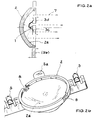
- the component shown in FIG. 1 consists of an optoelectronic semiconductor chip 1, which can either be a radiation-sensitive receiver or a radiation-emitting emitter.
- an optoelectronic semiconductor chip 1 can either be a radiation-sensitive receiver or a radiation-emitting emitter.
- only the light path 7 is to be reversed or radiated and detected radiation powers are exchanged, etc.
- the semiconductor chip 1 is mounted on a carrier strip 3.
- the carrier strip 3 consists of two essentially parallel legs 3a, 3b.
- the leg 3a has a branch 3c which points in the direction of the other leg.
- the branch 3c of the one leg extends somewhat further than to the axis of symmetry of the reflector.
- the semiconductor chip is attached to the free end of this branch 3c in the center of the reflector and is electrically connected to both parts of the carrier strip.
- this is advantageously carried out on the basis of the rear-side contact for the partial strip 3c on which the semiconductor chip 1 is mounted.
- the electrical connection to the other sub-strip 3d is made by means of a bonding wire. It is of course also possible to contact both connections with bonding wires, in particular when the two electrical connections of the semiconductor chip 1 are arranged on the upper side thereof. Furthermore, it is possible to lead the strip 3d to the center of the reflector and to mount the chip there.
- the leads 3a, 3b of the two partial strips are connected with webs.
- the ends are only cut free after the component has been cast, creating two separate connections.
- a reflector 2 is attached to the carrier strip 3 in such a way that the semiconductor chip 1 is as close as possible to the focal point of the parabolic reflector 2.
- the reflector 2 has latching elements 5, into which the carrier strip is firmly locked.
- the entire arrangement is surrounded by a housing 4, a part of the carrier strip 3a, 3b protruding from the housing 4 and serving as connection and mounting legs for the component.
- the housing 4 advantageously consists of a translucent plastic and is produced, for example, by casting the arrangement with a synthetic resin compound.
- the semiconductor chip 1 and the carrier strip 3 are produced by means of customary method steps.
- the carrier strip already has the shape shown in FIG. 1, with the exception that the two partial strips on the two lower legs 3a, 3b, which later form the connecting legs, are connected to one another by webs. At the other end, one of the two partial strips has a branch 3c which approaches the other strip 3d.
- the semiconductor chip is mounted on the strip part 3c or 3d which projects into the center of the reflector. If the semiconductor chip has a backside contact, the assembly is carried out by soldering or gluing with a conductive plastic adhesive. With this procedure, electrical contact is simultaneously created with the one partial strip 3c of the carrier strip.
- the second electrical contact is made by wire bonding.
- a contact of the semiconductor chip lying on the upper side is connected to the second partial strip.
- the semiconductor chip is glued onto the longer branch 3c.
- the electrical contacts of the semiconductor chip are then connected to the partial strips. This is expediently carried out using a known wire bonding method.
- the reflector 2 is connected to the contact strip 3, so that the semiconductor chip faces the reflector and, if possible, comes to lie in its focal point.
- the reflector is equipped with locking elements 5, and the carrier strip 3 is only snapped into the locking elements 5 in the correct position. To facilitate positioning, positioning aids such as conical tips of the latching hooks can be provided.
- the arrangement is provided with a translucent housing 4. This is done by a known method such as. B. casting in a synthetic resin compound. The arrangement is completely potted. Only the ends 3a, 3b of the carrier strip which are determined as connecting legs remain free. The connecting webs described above, which gave the arrangement the necessary strength during assembly, are finally removed.
- the optoelectronic component produced in this way has a small dimension in the direction of radiation or irradiation with a very small opening angle. Furthermore, a very high beam parallelism and a very large aperture angle are achieved in the component according to the invention.
- FIGS. 1 and 2 which can be used both as optoemitters and optodetectors, can be used to produce an optocoupler according to FIG. 3, where with the reference numerals 10 and 11 an optoemitter or an optodetector are designated.
- the individual parts of these components are designated by the corresponding reference numerals from FIGS. 1 and 2, those reference numerals of the optoemitter 10 being untracked and those reference numerals of the optodetector 11 being deleted. It can now be seen from FIG.
- each chip that is to say the emitter chip 1 and also the detector chip 1 ', lies in a Faraday cage which is formed from the reflector 2 or 2' and the carrier strip 3 or 3 '.
- the surface 2a or 2a 'of the reflector 2 or 2' is metallized, which is in each case electrically conductively connected to a part 3a or 3b or 3a 'or 3b' of the associated carrier strip 3 or 3 'in order to achieve the effect of a Faraday cage.
- the electrical field generated by the isolating voltage between the receiver and transmitter sides can thus be shielded, so that a high dielectric strength is ensured in the long term.
- the radiation 7 emitted by the emitter chip 1 is almost completely focused on the detector chip 1 ', making it possible to use very small receiver chips, which leads to leads to a cost reduction in the manufacture of the optocoupler.
- the same cause also has the advantage that the distance between the two components 10 and 11 can be increased without a great influence on the coupling factor.
Landscapes
- Engineering & Computer Science (AREA)
- Microelectronics & Electronic Packaging (AREA)
- Power Engineering (AREA)
- Computer Hardware Design (AREA)
- Condensed Matter Physics & Semiconductors (AREA)
- Physics & Mathematics (AREA)
- Manufacturing & Machinery (AREA)
- Electromagnetism (AREA)
- General Physics & Mathematics (AREA)
- Led Device Packages (AREA)
- Photo Coupler, Interrupter, Optical-To-Optical Conversion Devices (AREA)
- Optical Communication System (AREA)
- Light Receiving Elements (AREA)
Description
Die Erfindung betrifft ein optoelektronisches Bauelement mit einem engen Öffnungswinkel nach dem Oberbegriff des Anspruchs 1. Weiterhin betrifft die Erfindung ein Verfahren zum Herstellen eines solchen Bauelements.The invention relates to an optoelectronic component with a narrow opening angle according to the preamble of
Konventionelle optoelektronische Halbleiterbauelemente, wie z. B. Leuchtdioden, weisen zur Einengung des Öffnungswinkels einschalige Linsen aus Plastik auf. Derartige Bauelemente sind z. B. in Gillessen, Schairer, "Light emitting diodes: an introduction", Prentice-Hall International, 1987, S. 217 - 219, Fig. 7-6 beschrieben. Diese konventionellen Bauteile weisen den Nachteil auf, daß eine Einengung des Abstrahlwinkels Ø mit der Vergrößerung der Brennweite f einhergeht. Gleichzeitig werden die Bauteilabmessungen in Abstrahlrichtung größer. Damit ursächlich verknüpft ist, daß bei vorgegebenem Linsen- und damit im allgemeinen auch Bauteildurchmesser der Aperturwinkel α kleiner wird und gleichzeitig, im Falle eines Optoemitters, die Nutzleistung zurückgeht. Im Falle eines Detektors reduziert sich die Menge der einfallenden Lichtleistung. Der allgemeine Zusammenhang zwischen dem Abstrahlwinkel Ø des Bauelements, der Brennweite f der Linse und dem Aperturwinkel α bei den bekannten Bauelementen ist in der Figur 4 dargestellt.Conventional optoelectronic semiconductor components, such as. B. LEDs, to narrow the opening angle on single-layer lenses made of plastic. Such components are such. B. in Gillessen, Schairer, "Light emitting diodes: an introduction", Prentice-Hall International, 1987, pp. 217-219, Fig. 7-6. These conventional components have the disadvantage that a narrowing of the beam angle Ø is accompanied by an increase in the focal length f. At the same time, the component dimensions become larger in the direction of radiation. This is causally linked to the fact that for a given lens diameter and thus generally also component diameter, the aperture angle α becomes smaller and, in the case of an optoemitter, the useful power decreases at the same time. In the case of a detector, the amount of incident light power is reduced. The general relationship between the beam angle Ø of the component, the focal length f of the lens and the aperture angle α in the known components is shown in FIG.
Aus der EP-A-0 364 806 ist ein optoelektronisches Bauelement bekannt, bei dem flächenhaft verteilte Lumineszenz-Halbleiterkörper durch eine Leitbahnstruktur miteinander verbunden und die einzelnen Lumineszenz-Halbleiterkörper von Gehäusekörper umgeben sind. Der Gehäusekörper entsteht durch einen Verguß mit einer transparenten Kunststoff-Vergußmasse. Die Gehäusekörper weisen eine parabolische Form auf, deren Außenflächen zur Bildung eines Reflektors mit einem hochreflektierenden Material beschichtet werden. Die Halbleiterkörper sind derart angordnet, daß sie jeweils im Brennpunkt eines Reflektors liegen.From EP-A-0 364 806 an optoelectronic component is known, in which areally distributed luminescent semiconductor bodies are connected to one another by an interconnect structure and the individual luminescent semiconductor bodies are surrounded by housing bodies. The housing body is created by potting with a transparent plastic potting compound. The housing bodies have a parabolic shape, the outer surfaces of which are coated with a highly reflective material to form a reflector will. The semiconductor bodies are arranged in such a way that they are each in the focal point of a reflector.
Aufgabe der Erfindung ist es daher, ein optoelektronisches Bauelement anzugeben, das einen engen Abstrahlwinkel aufweist, sich gleichzeitig durch geringe Bautiefe und hohe Leistungsausbeute auszeichnet und auf einfache Art herzustellen ist.It is therefore an object of the invention to provide an optoelectronic component which has a narrow beam angle, is at the same time distinguished by a low structural depth and high power yield and can be produced in a simple manner.
Diese Aufgabe wird durch ein Bauelement mit den kennzeichnenden Merkmalen des Anspruchs 1 gelöst.This object is achieved by a component with the characterizing features of
Es ist eine weitere Aufgabe der Erfindung, ein Verfahren anzugeben, nach dem das erfindungsgemäße Bauelement herzustellen ist.It is a further object of the invention to specify a method by which the component according to the invention is to be manufactured.
Diese Aufgabe wird durch ein Verfahren mit den kennzeichnenden Merkmalen des Anspruchs 6 gelöst.This object is achieved by a method with the characterizing features of claim 6.
Vorteilhafte Ausgestaltungen des Bauelements und des Verfahrens zum Herstellen des Bauelements ergeben sich aus den unteransprüchen.Advantageous refinements of the component and of the method for producing the component result from the subclaims.
Insbesondere kann gemäß Anspruch 7 das erfindungsgemäße optoelektronische Bauelement zum Aufbau eines Optokopplers verwendet werden. Hierzu wird ein Optoemitter und ein Optodetektor gemäß der Erfindung einander gegenübergestellt und über ein Gehäuse optisch und mechanisch gekoppelt.In particular, according to
Bei einer solchen Anordnung befinden sich der Emitter- und Detektorchip in einem Faraday'schen Käfig, der durch den metallischen Montagestreifen und den metallischen Reflektor gebildet wird. Folglich befindet sich jeder der beiden Chips in einem nahezu feldfreien Raum, unabhängig von der anliegenden Spannung.In such an arrangement, the emitter and detector chip are located in a Faraday cage, which is formed by the metallic mounting strip and the metallic reflector. As a result, each of the two chips is located in an almost field-free space, regardless of the voltage applied.
Dies führt bei einem solchen Optokoppler zu einer wesentlichen Verbesserung der langfristigen Spannungsfestigkeit. Denn die über einen langen Zeitraum anliegende Gleichspannung bedeutet eine starke Belastung der Chips, insbesondere des Detektorchips. Die Belastung ist um so größer, je höher die Spannung, je höher die Temperatur und je länger die Zeit ist, während welcher alle Änderungen der Funktionsdaten unterhalb einer vorgegebenen Grenze bleiben sollen.With such an optocoupler, this leads to a significant improvement in the long-term dielectric strength. This is because the DC voltage that is present over a long period of time means that the chips, in particular the detector chip, are under high stress. The load is greater, the higher the voltage, the higher the temperature and the longer the time during which all changes in the functional data should remain below a predetermined limit.
Die genannte Belastung kommt dadurch zustande, daß auf Ladungen in den Passivierungsschichten unter dem Einfluß der durch die Spannung bestimmten Feldstärke eine Kraft wirkt. Falls es zur Bewegung von Ladungen kommt, reichern sich diese an den Grenzflächen der Passivierung an. Es kann zu Verarmungsschichten oder sogar Inversionsschichten im angrenzenden Siliziummaterial kommen, die die Funktionsdaten des Chips verändern können.The aforementioned load is caused by the fact that a force acts on charges in the passivation layers under the influence of the field strength determined by the voltage. If charges move, these accumulate at the passivation interfaces. Depletion layers or even inversion layers can occur in the adjacent silicon material, which can change the functional data of the chip.
Zu entsprechenden Effekten kann es selbst im Falle stabiler Passivierungsschichten durch den die Chips einbettenden Kunststoff kommen. Enthält der Kunststoff Ladungen, so werden auch diese zur Wanderung tendieren, sich gegebenenfalls an der Oberfläche der Halbleiterchips anreichern und je nach der Auslegung dieser Chips zu mehr oder weniger großen Änderungen der Meßdaten führen.Corresponding effects can occur even in the case of stable passivation layers through the plastic embedding the chips. If the plastic contains charges, they will also tend to migrate, possibly accumulate on the surface of the semiconductor chips and, depending on the design of these chips, lead to more or less large changes in the measurement data.
Da die Chips des oben beschriebenen Optokopplers, der mit den erfindungsgemäßen optoelektronischen Bauelementen aufgebaut ist, in einem nahezu feldfreien Raum liegen, werden von diesen die oben beschriebenen Belastungen ferngehalten. Insbesondere bei Hochspannungskopplern, bei denen Spannungsspitzenwerte von mehr als 5 kVss auftreten können, wird das durch diese Spannung hervorgerufene Feld abgeschirmt.Since the chips of the optocoupler described above, which is constructed with the optoelectronic components according to the invention, are located in an almost field-free space, the loads described above are kept away from them. In particular in the case of high-voltage couplers, in which voltage peak values of more than 5 kV ss can occur, the field caused by this voltage is shielded.
Eine solche Lösung ist gegenüber bekannten Optokopplern billig und von wesentlich höherer Wirksamkeit. Ferner ist vorteilhaft, daß bei einem solchen Optokoppler sehr kleine Empfängerchips einsetzbar sind und der Abstand des Optoemitters und des Optodetektors ohne großen Einfluß auf den Koppelfaktor infolge des engen Öffnungswinkels der Bauelemente vergrößerbar ist. Schließlich ergibt sich trotz des großen Abstandes eine relativ kurze Baulänge des Optokopplers.Such a solution is inexpensive compared to known optocouplers and is considerably more effective. It is also advantageous that very small receiver chips can be used with such an optocoupler and that the distance between the optoemitter and the optodetector can be increased without great influence on the coupling factor due to the narrow opening angle of the components. Finally, despite the large distance, the optocoupler has a relatively short overall length.
Die Erfindung sei im nachfolgenden anhand der Figuren 1 und 2 erläutert. Dabei zeigt die
- Figur 1a
- die Seitenansicht einer vorteilhaften Ausführung des Bauelements,
- Figur 1b
- die Vorderansicht der in Figur 1a dargestellten Ausführung,
Figur 2- die genaue Form des Reflektors,
Figur 3- eine Seitenansicht eines mit erfindungsgemäßen optoelektronischen Bauelementen aufgebauten Optokopplers.
- Figure 1a
- the side view of an advantageous embodiment of the component,
- Figure 1b
- the front view of the embodiment shown in Figure 1a,
- Figure 2
- the exact shape of the reflector,
- Figure 3
- a side view of an optocoupler constructed with optoelectronic components according to the invention.
Das in Figur 1 dargestellte Bauelement besteht aus einem optoelektronischen Halbleiterchip 1, der entweder ein auf Strahlung ansprechender Empfänger oder ein Strahlung aussendender Emitter sein kann. Für beide Ausführungsformen, Optoemitter und Optodetektor, gilt nachfolgendes in äquivalenter Weise. Bei den Betrachtungen sind lediglich der Lichtweg 7 umzukehren bzw. abgestrahlte und detektierte Strahlungsleistungen auszutauschen, etc.The component shown in FIG. 1 consists of an
Der Halbleiterchip 1 ist auf einem Trägerstreifen 3 aufmontiert. Der Trägerstreifen 3 besteht im Ausführungsbeispiel aus zwei im wesentlichen parallelen Schenkeln 3a, 3b. Im oberen Bereich weist der Schenkel 3a eine Abzweigung 3c auf, die in Richtung des anderen Schenkels weist. Die Abzweigung 3c des einen Schenkels reicht etwas weiter als bis zur Symmetrieachse des Reflektors. Der Halbleiterchip ist am freien Ende dieser Abzweigung 3c im Zentrum des Reflektors angebracht und mit beiden Teilen des Trägerstreifens elektrisch verbunden. Dies erfolgt vorteilhaft einerseits anhand des Rückseitenkontakts für den Teilstreifen 3c, auf dem der Halbleiterchip 1 montiert ist. Der elektrische Anschluß zum anderen Teilstreifen 3d erfolgt mittels eines Bonddrahtes. Es ist natürlich auch möglich, beide Anschlüsse mit Bonddrähten zu kontaktieren, insbesondere dann, wenn die beiden elektrischen Anschlüsse des Halbleiterchips 1 auf dessen Oberseite angeordnet sind. Des weiteren ist es möglich, den Streifen 3d bis ins Zentrum des Reflektors zu führen und dort den Chip zu montieren.The
Zum Zeitpunkt der Montage des Halbleiterchips und des Reflektors sind die Zuleitungen 3a, 3b der beiden Teilstreifen mit Stegen verbunden. Erst nachdem das Bauteil vergossen ist, werden die Enden freigeschnitten, wodurch zwei separate Anschlüsse entstehen.At the time of assembling the semiconductor chip and the reflector, the
Auf den Trägerstreifen 3 ist ein Reflektor 2 derart angebracht, daß das Halbleiterchip 1 möglichst im Brennpunkt des parabolischen Reflektors 2 liegt. Der Reflektor 2 weist gemäß der Erfindung Rastelemente 5 auf, in die der Trägerstreifen fest eingerastet ist.A
Die gesamte Anordnung ist von einem Gehäuse 4 umgeben, wobei ein Teil des Trägerstreifens 3a, 3b aus dem Gehäuse 4 herausragt und als Anschluß- und Montagebeinchen für das Bauelement dient. Das Gehäuse 4 besteht vorteilhaft aus einem lichtdurchlässigen Kunststoff und wird beispielsweise durch Vergießen der Anordnung mit einer Kunstharzmasse hergestellt.The entire arrangement is surrounded by a
Nachfolgend sei ein Verfahren zum Herstellen des oben beschriebenen Bauelements beschrieben. Zunächst wird mittels üblicher Verfahrensschritte der Halbleiterchip 1 und der Trägerstreifen 3 hergestellt. Der Trägerstreifen weist dabei schon die in der Figur 1 gezeigte Form auf, mit der Ausnahme, daß die beiden Teilstreifen an den beiden unteren Schenkeln 3a, 3b, die später die Anschlußbeinchen bilden, durch Stege miteinander verbunden sind. Am anderen Ende weist einer der beiden Teilstreifen eine Abzweigung 3c auf, die sich dem anderen Streifen 3d annähert. Auf den bis ins Zentrum des Reflektors ragenden Streifenteil 3c oder 3d wird der Halbleiterchip montiert. Weist der Halbleiterchip einen Rückseitenkontakt auf, erfolgt die Montage durch Verlöten oder Verkleben mit einem leitfähigen Kunststoffkleber. Bei dieser Vorgehensweise wird gleichzeitig ein elektrischer Kontakt zu dem einen Teilstreifen 3c des Trägerstreifens geschaffen. Der zweite elektrische Kontakt wird durch ein Drahtbondverfahren hergestellt. Dabei wird ein auf der Oberseite liegender Kontakt des Halbleiterchips mit dem zweiten Teilstreifen verbunden. In einer anderer Ausführung wird der Halbleiterchip auf die längere Abzweigung 3c aufgeklebt. Anschließend werden die elektrischen Kontakte des Halbleiterchips mit den Teilstreifen verbunden. Dies erfolgt zweckmäßigerweise durch ein bekanntes Drahtbondverfahren. Im nächsten Verfahrensschritt wird der Reflektor 2 mit dem Kontaktstreifen 3 verbunden, so daß der Halbleiterchip dem Reflektor zugewandt ist und möglichst in dessen Brennpunkt zu liegen kommt. Der Reflektor ist mit Rastelementen 5 ausgerüstet, und der Trägerstreifen 3 wird lediglich positionsgenau in die Rastelemente 5 eingerastet. Um das Positionieren zu erleichtern, können Positionierhilfen wie kegelförmige Spitzen der Rasthaken vorgesehen sein.A method for producing the component described above will be described below. First, the
Abschließend wird die Anordnung mit einem lichtdurchlässigen Gehäuse 4 versehen. Dies erfolgt durch ein an sich bekanntes Verfahren wie z. B. das Vergießen in einer Kunstharzmasse. Die Anordnung wird vollständig vergossen. Lediglich die als Anschlußbeinchen bestimmten Enden 3a, 3b des Trägerstreifens bleiben frei. Die oben beschriebenen Verbindungsstege, die der Anordnung während der Montage die nötige Festigkeit verliehen haben, werden abschließend noch entfernt.Finally, the arrangement is provided with a
Das auf diese Weise hergestellte optoelektronische Bauelement weist eine geringe Abmessung in Ab- bzw. Einstrahlrichtung bei einem sehr kleinen Öffnungswinkel auf. Weiterhin wird bei dem erfindungsgemäßen Bauelement eine sehr hohe Strahlparallelität und ein sehr großer Aperturwinkel erzielt.The optoelectronic component produced in this way has a small dimension in the direction of radiation or irradiation with a very small opening angle. Furthermore, a very high beam parallelism and a very large aperture angle are achieved in the component according to the invention.
Die in den Figuren 1 und 2 beschriebenen erfindungsgemäßen optoelektronischen Bauelemente, die sowohl als Optoemitter als auch Optodetektor verwendbar sind, können zur Herstellung eines Optokopplers gemäß der Figur 3 verwendet werden, wo mit den Bezugszeichen 10 und 11 ein Optoemitter bzw. ein Optodetektor bezeichnet sind. Die einzelnen Teile dieser Bauelemente sind mit den entsprechenden Bezugszeichen aus den Figuren 1 und 2 bezeichnet, wobei diejenigen Bezugszeichen des Optoemitters 10 ungestrichen und diejenigen Bezugszeichen des Optodetektors 11 gestrichen sind. Anhand der Figur 3 ist nun ersichtlich, daß jeder Chip, also der Emitterchip 1 als auch der Detektorchip 1' in einem Faraday'schen Käfig liegt, der aus dem Reflektor 2 bzw. 2' und dem Trägerstreifen 3 bzw. 3' gebildet ist. Dabei ist jeweils die Oberfläche 2a bzw. 2a' des Reflektors 2 bzw. 2' metallisiert, die jeweils mit einem Teil 3a oder 3b bzw. 3a' oder 3b' des zugehörigen Trägerstreifens 3 bzw. 3' elektrisch leitend verbunden ist, um die Wirkung eines Faraday'schen Käfigs sicherzustellen. Somit kann das von der zwischen der Empfänger- und Senderseite liegenden Trennspannung erzeugte elektrische Feld abgeschirmt werden, so daß langfristig eine hohe Spannungsfestigkeit sichergestellt ist.The optoelectronic components according to the invention described in FIGS. 1 and 2, which can be used both as optoemitters and optodetectors, can be used to produce an optocoupler according to FIG. 3, where with the
Dadurch, daß die jeweiligen Chips 1 und 1' im Brennpunkt der Reflektoren 1 und 1' liegen, wird die von dem Emitterchip 1 abgegebene Strahlung 7 nahezu vollständig auf den Detektorchip 1' fokussiert, womit es möglich ist, sehr kleine Empfängerchips einzusetzen, was zu einer Kostenreduzierung bei der Herstellung des Optokopplers führt. Auf die gleiche Ursache ist auch der Vorteil zurückzuführen, daß der Abstand zwischen den beiden Bauelementen 10 und 11 ohne großen Einfluß auf den Koppelfaktor vergrößerbar ist.Characterized in that the
Claims (7)
- An optoelectronic component with a narrow opening angle comprising a semiconductor chip (1) which transmits radiation or responds to radiation and which is mounted on a carrier strip (3), where a parabolic or approximately parabolic reflector (20 is provided which is connected to the carrier strip (3) in such manner that the semiconductor chip (1) mounted on the carrier strip (3) is situated as far as possible at the focal point of the parabolic or approximately parabolic surface (2a) of the reflector (2), characterised in that the reflector (2) comprises locking elements (5) into which the carrier strip (3) is engaged.
- An optoelectronic component according to Claim 1, characterised in that the semiconductor chip (1) is mounted on that side of the carrier strip (3) which faces towards the reflector (2).
- An optoelectronic component according to Claim 1 or 2, characterised in that the reflector (2) is composed of a plastics material, where at least one surface is coated with a highly reflective metal.
- An optoelectronic component according to one of Claims 1 to 3, characterised in that the reflector (2), the semiconductor chip (1) and parts of the carrier strip (3) are completely surrounded by a light-transmissive housing (4) and that only those ends of the carrier strip (3) which serve as terminal legs (3a, 3b) project from the housing.
- An optoelectronic component according to one of Claims 1 to 4, characterised in that the carrier strip (3) comprises two sub-strips (3a, 3b) and that only one of the two sub-strips (3a or 3b) is in contact with the reflector (2).
- A process for the production of an optoelectronic component with a narrow opening angle, in the course of which a semiconductor chip (1) is mounted on a carrier strip (3) and electric contacts are established between the semiconductor chip (1) and the carrier strip (3), where a reflector (2) is arranged in such manner that the semiconductor chip (1) faces towards the reflector (2) and is situated substantially at the focal point thereof, characterised in that the reflector (2) comprises locking elements (5), and that prior to the construction of a housing (4) the reflector is connected to the carrier strip in that upon assembly the carrier strip (3) is engaged into the locking elements.
- The use of the optoelectronic component according to one of Claims 1 to 5 for the production of an opto-coupler constructed from an opto-emitter (10) and an opto-detector (11), where the reflector (2, 2') both of the opto-emitter (10) and of the opto-detector (11) comprises a metallisation and the said metallisation of each reflector (2, 2') is in each case electrically conductively connected to one of the two parts (3a, 3b; 3a', 3b') of the associated carrier strip (3, 3') which bears the emitter chip (1) or the detector chip (1').
Applications Claiming Priority (4)
| Application Number | Priority Date | Filing Date | Title |
|---|---|---|---|
| DE4233125 | 1992-10-02 | ||
| DE4233125 | 1992-10-02 | ||
| DE4311530A DE4311530A1 (en) | 1992-10-02 | 1993-04-07 | Optoelectronic component with a narrow opening angle |
| DE4311530 | 1993-04-07 |
Publications (2)
| Publication Number | Publication Date |
|---|---|
| EP0590336A1 EP0590336A1 (en) | 1994-04-06 |
| EP0590336B1 true EP0590336B1 (en) | 1997-03-05 |
Family
ID=25919111
Family Applications (1)
| Application Number | Title | Priority Date | Filing Date |
|---|---|---|---|
| EP93114017A Expired - Lifetime EP0590336B1 (en) | 1992-10-02 | 1993-09-02 | Optoelectronic element with narrow beam angle |
Country Status (4)
| Country | Link |
|---|---|
| US (2) | US5384471A (en) |
| EP (1) | EP0590336B1 (en) |
| JP (1) | JPH06209124A (en) |
| DE (2) | DE4311530A1 (en) |
Families Citing this family (22)
| Publication number | Priority date | Publication date | Assignee | Title |
|---|---|---|---|---|
| JPH07335980A (en) * | 1994-06-07 | 1995-12-22 | Fuji Electric Co Ltd | Semiconductor laser device |
| CN1047691C (en) * | 1994-08-26 | 1999-12-22 | 张龙宝 | Color freely changeable fully-centralied extra-high photo effect solid photo source |
| US5723363A (en) * | 1995-09-29 | 1998-03-03 | Siemens Components, Inc. | Method of manufacturing a semiconductor device |
| DE19610881B4 (en) * | 1995-12-07 | 2008-01-10 | Limo Patentverwaltung Gmbh & Co. Kg | Microsystem module |
| US5808325A (en) * | 1996-06-28 | 1998-09-15 | Motorola, Inc. | Optical transmitter package assembly including lead frame having exposed flange with key |
| JP3970377B2 (en) * | 1997-04-25 | 2007-09-05 | 沖電気工業株式会社 | Optical semiconductor device and manufacturing method thereof |
| DE19829197C2 (en) * | 1998-06-30 | 2002-06-20 | Siemens Ag | Component emitting and / or receiving radiation |
| JP3857435B2 (en) * | 1998-08-31 | 2006-12-13 | ローム株式会社 | Optical semiconductor element, optical semiconductor element mounting structure, and optical semiconductor element group packaging structure |
| US6335548B1 (en) * | 1999-03-15 | 2002-01-01 | Gentex Corporation | Semiconductor radiation emitter package |
| EP1113506A3 (en) | 1999-12-28 | 2005-03-16 | Toyoda Gosei Co., Ltd. | Light emitting diode |
| EP1244152A3 (en) * | 2001-01-26 | 2008-12-03 | Toyoda Gosei Co., Ltd. | Reflective light emitting diode, reflective optical device and its manufacturing method |
| JP4388806B2 (en) * | 2001-08-21 | 2009-12-24 | オスラム オプト セミコンダクターズ ゲゼルシャフト ミット ベシュレンクテル ハフツング | Casing and conductor frame for radiation emitting component, radiation emitting component, display device and / or illumination device with radiation emitting component |
| DE10147986A1 (en) * | 2001-09-28 | 2003-04-10 | Osram Opto Semiconductors Gmbh | Manufacturing surface mountable light emitting diode light source involves bending leadframe reflector section into shape of reflector before or after mounting LED chip |
| JP3982635B2 (en) * | 2003-04-16 | 2007-09-26 | 株式会社 オプトデバイス研究所 | Reflective light emitting diode |
| DE112004002083T5 (en) * | 2003-10-31 | 2008-03-20 | Toyoda Gosei Co., Ltd. | Light-emitting device |
| US7230280B2 (en) * | 2004-05-27 | 2007-06-12 | Avago Technologies Ecbu Ip (Singapore) Pte. Ltd. | Collimating light from an LED device |
| US8070329B1 (en) | 2005-02-11 | 2011-12-06 | Gentex Corporation | Light emitting optical systems and assemblies and systems incorporating the same |
| US7796403B2 (en) * | 2006-09-28 | 2010-09-14 | Nellcor Puritan Bennett Llc | Means for mechanical registration and mechanical-electrical coupling of a faraday shield to a photodetector and an electrical circuit |
| KR101470997B1 (en) * | 2008-05-13 | 2014-12-09 | 가부시키가이샤 플래너즈 랜드 | Reflective collection-type light receiving unit and light receiving apparatus for spatial light communications |
| US8858032B2 (en) * | 2008-10-24 | 2014-10-14 | Cree, Inc. | Lighting device, heat transfer structure and heat transfer element |
| JP5488310B2 (en) * | 2010-07-30 | 2014-05-14 | 市光工業株式会社 | Light source unit of semiconductor light source for vehicle lamp, vehicle lamp |
| JP5786693B2 (en) * | 2011-01-14 | 2015-09-30 | 株式会社デンソー | Air conditioner |
Family Cites Families (36)
| Publication number | Priority date | Publication date | Assignee | Title |
|---|---|---|---|---|
| DE883105C (en) * | 1951-11-10 | 1953-07-13 | Lorenz C Ag | Device for modulating a light beam |
| US3727064A (en) * | 1971-03-17 | 1973-04-10 | Monsanto Co | Opto-isolator devices and method for the fabrication thereof |
| CA917812A (en) * | 1971-05-14 | 1972-12-26 | Dennis Effer | Package for light emitting devices |
| SU434873A1 (en) * | 1971-07-13 | 1977-08-25 | Ордена Ленина Физико-Технический Институт Имени А.Ф.Иоффе Ан Ссср | Optoelectronic device |
| JPS48100083A (en) * | 1972-02-24 | 1973-12-18 | ||
| GB1383548A (en) * | 1972-06-29 | 1974-02-12 | Plessey Co Ltd | Light emitting diode assembly |
| FR2262407B1 (en) * | 1974-02-22 | 1977-09-16 | Radiotechnique Compelec | |
| FR2287108A1 (en) * | 1974-10-01 | 1976-04-30 | Radiotechnique Compelec | OPTOELECTRONIC DEVICE WITH TRANSMITTER AND RECEIVER COUPLES |
| US4114177A (en) * | 1975-05-01 | 1978-09-12 | Bell Telephone Laboratories, Incorporated | Optically coupled device with diffusely reflecting enclosure |
| US4110608A (en) * | 1976-11-04 | 1978-08-29 | Electronics Corporation Of America | Two-terminal photodetectors with inherent AC amplification properties |
| US4203792A (en) * | 1977-11-17 | 1980-05-20 | Bell Telephone Laboratories, Incorporated | Method for the fabrication of devices including polymeric materials |
| DE2806167C2 (en) * | 1978-02-14 | 1986-05-15 | Siemens AG, 1000 Berlin und 8000 München | High voltage resistant optocoupler |
| US4271408A (en) * | 1978-10-17 | 1981-06-02 | Stanley Electric Co., Ltd. | Colored-light emitting display |
| US4317232A (en) * | 1979-01-12 | 1982-02-23 | Deere & Company | Fiber optic signal conditioning circuit |
| DE3137685C2 (en) * | 1981-09-22 | 1983-11-03 | Siemens AG, 1000 Berlin und 8000 München | Light emitting diode for signal lights. |
| DE3316271A1 (en) * | 1983-04-29 | 1984-10-31 | Licentia Patent-Verwaltungs-Gmbh, 6000 Frankfurt | Arrangement for planar optocoupling |
| JPS6195581A (en) * | 1984-10-16 | 1986-05-14 | Toshiba Corp | Photocoupler |
| AU594397B2 (en) * | 1985-10-29 | 1990-03-08 | Interactive Devices Pty. Ltd. | Touch sensitive indicating light |
| DE3633181C2 (en) * | 1986-09-30 | 1998-12-10 | Siemens Ag | Reflex light barrier |
| DE3732075A1 (en) * | 1987-09-23 | 1989-04-06 | Siemens Ag | HERMETICALLY SEALED GLASS METAL HOUSING FOR SEMICONDUCTOR COMPONENTS AND METHOD FOR THE PRODUCTION THEREOF |
| JPH01230274A (en) * | 1987-11-13 | 1989-09-13 | Iwasaki Electric Co Ltd | Light emitting diode |
| JP2730042B2 (en) * | 1988-03-14 | 1998-03-25 | 岩崎電気株式会社 | Transmission type photo sensor |
| JPH01241184A (en) * | 1988-03-23 | 1989-09-26 | Iwasaki Electric Co Ltd | Reflection type photosensor |
| JP2782717B2 (en) * | 1988-04-26 | 1998-08-06 | 岩崎電気株式会社 | Light emitting diode |
| JPH02105586A (en) * | 1988-10-14 | 1990-04-18 | Nec Corp | Photocoupler |
| DE3835942A1 (en) * | 1988-10-21 | 1990-04-26 | Telefunken Electronic Gmbh | AREA SPOTLIGHT |
| JP2707498B2 (en) * | 1988-11-11 | 1998-01-28 | 岩崎電気株式会社 | Light emitting diode |
| JP2787300B2 (en) * | 1989-04-21 | 1998-08-13 | 岩崎電気株式会社 | Light emitting diode |
| JPH0817467B2 (en) * | 1989-04-27 | 1996-02-21 | 三菱電機株式会社 | TV image display device |
| DE58909875D1 (en) * | 1989-05-31 | 2000-08-31 | Osram Opto Semiconductors Gmbh | Method for mounting a surface mount opto component |
| JPH0372683A (en) * | 1989-08-11 | 1991-03-27 | Toshiba Corp | Reflection type sensor |
| JPH03151674A (en) * | 1989-11-08 | 1991-06-27 | Sharp Corp | Semiconductor device |
| EP0450560B1 (en) * | 1990-04-03 | 1998-07-22 | Sumitomo Electric Industries, Ltd. | An optical device |
| JPH03288478A (en) * | 1990-04-04 | 1991-12-18 | Sumitomo Electric Ind Ltd | Light emitting element |
| US5119174A (en) * | 1990-10-26 | 1992-06-02 | Chen Der Jong | Light emitting diode display with PCB base |
| US5216805A (en) * | 1990-12-12 | 1993-06-08 | Eastman Kodak Company | Method of manufacturing an optoelectronic device package |
-
1993
- 1993-04-07 DE DE4311530A patent/DE4311530A1/en not_active Ceased
- 1993-09-02 DE DE59305586T patent/DE59305586D1/en not_active Expired - Lifetime
- 1993-09-02 EP EP93114017A patent/EP0590336B1/en not_active Expired - Lifetime
- 1993-09-28 JP JP27393793A patent/JPH06209124A/en active Pending
- 1993-09-30 US US08/128,659 patent/US5384471A/en not_active Expired - Lifetime
-
1994
- 1994-09-16 US US08/306,942 patent/US5472915A/en not_active Expired - Lifetime
Also Published As
| Publication number | Publication date |
|---|---|
| US5472915A (en) | 1995-12-05 |
| JPH06209124A (en) | 1994-07-26 |
| US5384471A (en) | 1995-01-24 |
| DE4311530A1 (en) | 1994-04-07 |
| DE59305586D1 (en) | 1997-04-10 |
| EP0590336A1 (en) | 1994-04-06 |
Similar Documents
| Publication | Publication Date | Title |
|---|---|---|
| EP0590336B1 (en) | Optoelectronic element with narrow beam angle | |
| DE69312358T2 (en) | Chip carrier for optical device | |
| EP1174745B1 (en) | Optoelectronic surface- mountable module | |
| DE69322821T2 (en) | Semiconductor protective housing for optical components | |
| EP1252540B1 (en) | Optical transmitting/receiving module comprising an internal optical waveguide | |
| DE102011113483B4 (en) | Method for producing a plurality of optoelectronic components and optoelectronic component | |
| DE102011116534B4 (en) | Radiation-emitting component | |
| DE3236567A1 (en) | OPTICAL COUPLER WITH A LEAD FRAME AND LEAD FRAME DAFUER | |
| EP0852816A2 (en) | Optoelectronic semiconductor component | |
| EP1095411A1 (en) | Radiation-emitting and/or -receiving component | |
| EP2062301A2 (en) | Housing for an optoelectronic component and arrangement of an optoelectronic component in a housing | |
| DE2950649C2 (en) | Optoelectronic coupling element | |
| DE3810899C2 (en) | ||
| WO2016202917A1 (en) | Method for producing an optoelectronic component and optoelectronic component | |
| DE2922949A1 (en) | DEVICE FOR CONNECTING AT LEAST ONE LIGHT-EMITTING DIODE TO AN OPTICAL LIGHT-GUIDE | |
| DE10004411A1 (en) | Electro-optical transmitter / receiver module and method for its production | |
| DE102013205594A1 (en) | Laser component and method for its production | |
| DE102012101463A1 (en) | Method for producing an optoelectronic component and thus produced optoelectronic component | |
| DE4133773C2 (en) | Optoelectronic device | |
| DE2721250A1 (en) | OPTOELECTRONICALLY COUPLED SEMICONDUCTOR ARRANGEMENT | |
| DE2431375C3 (en) | Method for producing an optoelectronic coupling element | |
| DE2253699B2 (en) | Semiconductor optocoupler and process for its manufacture | |
| EP0568838A1 (en) | Method of manufacturing an optoelectronic coupling element | |
| WO2015039808A1 (en) | Optoelectronic light-emitting component and leadframe assemblage | |
| EP0071917B1 (en) | Electrical device, group of devices, or integrated circuit, the active part of which is placed on a metal support, and process for its or their manufacture |
Legal Events
| Date | Code | Title | Description |
|---|---|---|---|
| PUAI | Public reference made under article 153(3) epc to a published international application that has entered the european phase |
Free format text: ORIGINAL CODE: 0009012 |
|
| AK | Designated contracting states |
Kind code of ref document: A1 Designated state(s): DE FR GB IT |
|
| 17P | Request for examination filed |
Effective date: 19940222 |
|
| 17Q | First examination report despatched |
Effective date: 19951023 |
|
| GRAG | Despatch of communication of intention to grant |
Free format text: ORIGINAL CODE: EPIDOS AGRA |
|
| GRAH | Despatch of communication of intention to grant a patent |
Free format text: ORIGINAL CODE: EPIDOS IGRA |
|
| GRAH | Despatch of communication of intention to grant a patent |
Free format text: ORIGINAL CODE: EPIDOS IGRA |
|
| GRAA | (expected) grant |
Free format text: ORIGINAL CODE: 0009210 |
|
| ITF | It: translation for a ep patent filed | ||
| AK | Designated contracting states |
Kind code of ref document: B1 Designated state(s): DE FR GB IT |
|
| GBT | Gb: translation of ep patent filed (gb section 77(6)(a)/1977) |
Effective date: 19970305 |
|
| REF | Corresponds to: |
Ref document number: 59305586 Country of ref document: DE Date of ref document: 19970410 |
|
| ET | Fr: translation filed | ||
| PLBE | No opposition filed within time limit |
Free format text: ORIGINAL CODE: 0009261 |
|
| STAA | Information on the status of an ep patent application or granted ep patent |
Free format text: STATUS: NO OPPOSITION FILED WITHIN TIME LIMIT |
|
| 26N | No opposition filed | ||
| REG | Reference to a national code |
Ref country code: GB Ref legal event code: 732E |
|
| REG | Reference to a national code |
Ref country code: FR Ref legal event code: TP |
|
| REG | Reference to a national code |
Ref country code: GB Ref legal event code: IF02 |
|
| PGFP | Annual fee paid to national office [announced via postgrant information from national office to epo] |
Ref country code: GB Payment date: 20120920 Year of fee payment: 20 |
|
| PGFP | Annual fee paid to national office [announced via postgrant information from national office to epo] |
Ref country code: DE Payment date: 20120921 Year of fee payment: 20 |
|
| PGFP | Annual fee paid to national office [announced via postgrant information from national office to epo] |
Ref country code: FR Payment date: 20121010 Year of fee payment: 20 |
|
| PGFP | Annual fee paid to national office [announced via postgrant information from national office to epo] |
Ref country code: IT Payment date: 20120926 Year of fee payment: 20 |
|
| REG | Reference to a national code |
Ref country code: DE Ref legal event code: R071 Ref document number: 59305586 Country of ref document: DE |
|
| REG | Reference to a national code |
Ref country code: GB Ref legal event code: PE20 Expiry date: 20130901 |
|
| PG25 | Lapsed in a contracting state [announced via postgrant information from national office to epo] |
Ref country code: DE Free format text: LAPSE BECAUSE OF EXPIRATION OF PROTECTION Effective date: 20130903 |
|
| PG25 | Lapsed in a contracting state [announced via postgrant information from national office to epo] |
Ref country code: GB Free format text: LAPSE BECAUSE OF EXPIRATION OF PROTECTION Effective date: 20130901 |