EP0588111A2 - Memory element - Google Patents
Memory element Download PDFInfo
- Publication number
- EP0588111A2 EP0588111A2 EP93113494A EP93113494A EP0588111A2 EP 0588111 A2 EP0588111 A2 EP 0588111A2 EP 93113494 A EP93113494 A EP 93113494A EP 93113494 A EP93113494 A EP 93113494A EP 0588111 A2 EP0588111 A2 EP 0588111A2
- Authority
- EP
- European Patent Office
- Prior art keywords
- transistor
- transistors
- transistor pair
- pair
- collector
- Prior art date
- Legal status (The legal status is an assumption and is not a legal conclusion. Google has not performed a legal analysis and makes no representation as to the accuracy of the status listed.)
- Granted
Links
Images
Classifications
-
- G—PHYSICS
- G11—INFORMATION STORAGE
- G11C—STATIC STORES
- G11C11/00—Digital stores characterised by the use of particular electric or magnetic storage elements; Storage elements therefor
- G11C11/21—Digital stores characterised by the use of particular electric or magnetic storage elements; Storage elements therefor using electric elements
- G11C11/34—Digital stores characterised by the use of particular electric or magnetic storage elements; Storage elements therefor using electric elements using semiconductor devices
- G11C11/40—Digital stores characterised by the use of particular electric or magnetic storage elements; Storage elements therefor using electric elements using semiconductor devices using transistors
- G11C11/41—Digital stores characterised by the use of particular electric or magnetic storage elements; Storage elements therefor using electric elements using semiconductor devices using transistors forming static cells with positive feedback, i.e. cells not needing refreshing or charge regeneration, e.g. bistable multivibrator or Schmitt trigger
- G11C11/411—Digital stores characterised by the use of particular electric or magnetic storage elements; Storage elements therefor using electric elements using semiconductor devices using transistors forming static cells with positive feedback, i.e. cells not needing refreshing or charge regeneration, e.g. bistable multivibrator or Schmitt trigger using bipolar transistors only
Definitions
- Such memory elements are preferably used in digital circuits which operate at a high clock frequency.
- the highest possible operating speed of the memory element is essentially determined by the capacitive load which is applied to the collectors of the transistors of the second and third transistor pairs coupled in pairs.
- These capacitances are composed primarily of the capacitance between the metallization and the substrate of the connecting lines to which the components connected to these circuit nodes are connected, and the capacitance between the collectors and the substrate of the connected transistors.
- the object of the invention is to provide a memory element with a set or reset function by which the switching speed of the memory element is not influenced.
- the memory element according to the invention contains a first transistor pair with the bipolar transistors 1, 2, the emitters of which are connected to one another and are connected via a current source 9 to a connection for a first supply potential VEE.
- the coupled emitters of a further pair of transistors made up of transistors 3, 4 and 5, 6 are connected to the collectors of transistors 1, 2.
- the collectors of the transistors of the further pairs of transistors are coupled in pairs. As shown in the figure, the collectors of the transistors 3, 5 to a node 24 and the collectors of the transistors 4, 6 connected to a node 25.
- the nodes 24, 25 are each connected to a connection for a second supply potential VCC via the series connection of a resistor 16 or 17 and the collector-emitter path of a transistor 7 or 8.
- Resistors 18 and 19 are connected to the collector circuit of transistors 7, 8.
- the collector-side connections of the resistors 18, 19 each have a connection 22 or 23 for an output signal A ⁇ or A on.
- the base connections of the transistors 7, 8 are controlled in each case via a resistor 20 or 21, which are connected to the connection for the supply potential VCC.
- the base connections of the transistors 1, 2 are connections for complementary signals C or C. ⁇ .
- the signal C is usually the clock signal of the memory element.
- the base connections of the transistors 3, 4 are connections for mutually complementary data signals D or D ⁇ .
- the base connections of the transistors 5, 6 are each fed back crosswise to the collectors of these transistors, that is to say the circuit nodes 25 and 24, respectively.
- a current switch made of transistors 30, 31 is provided, the coupled emitters of which are connected via a current source 32 to the connection for the supply potential VEE.
- the collector of the transistor 30 is connected to the connection for the supply potential VCC, the collector of the transistor 31 to the base of the transistor 8.
- the base connections of the transistors 31, 30 are replaced by complementary reset signals R and R ⁇ controlled.
- the operation of the memory element is explained below.
- the transistor 1 is conductive, the transistor 2 is blocked. If that For example, if data signal D is high, transistor 3 is conductive and transistor 4 is blocked.
- the current impressed by the current source 9 then flows via the path of the transistors 3, 1 and via the path of the resistors 16, 18 and the transistor 7.
- the resistor 18 is dimensioned such that the level of the output signal A ⁇ is an L level at output 22.
- the resistor 19 is without current, so that the output signal A at the output 23 is H.
- the output signal A ⁇ is therefore complementary to the data signal D, the output signal A in the same direction.
- the transistors 7, 8 are connected in an emitter follower circuit with respect to the supply potential VCC.
- the potential at the emitters of transistors 7, 8 is consequently constant and is composed of the voltage drop across resistors 20 and 21 and the base-emitter voltages of transistors 7 and 8, respectively.
- the signals A or A ⁇ decoupled from the corresponding signals at the circuit nodes 25 and 24.
- the value of the inductance of the transistors 7, 8 can be set via the resistors 20 and 21, respectively.
- the reset signal R is initially L.
- the transistor 31 is then blocked, so that the base potential of the transistor 8 is unaffected and the switching state of the memory element is retained. Now the reset signal R is set to H.
- the transistor 31 is conductive, the transistor 30 is blocked. This lowers the potential at the base of transistor 8, so that - the clock signal C is L - the current switch of transistors 5, 6 switches over.
- the transistor 5 is blocked due to its now low base potential, the transistor 6 conducts.
- the output signal A switches to L.
- the memory element is therefore reset by an H level of the reset signal R.
- a current switch corresponding to the current switch comprising the transistors 30, 31 and the current source 32, is necessary, in which the collector connection of one of the transistors is connected to the base connection of the transistor 7. If this transistor is controlled to be conductive, the base potential of transistor 7 is lowered to such an extent that transistor 6 is blocked and transistor 5 is conductive. The output signal A is then H. If the memory element has a set and reset function, a power switch is required for the set and reset function.
- the current switch according to the invention has the advantage that the nodes 24, 25 are not additionally loaded capacitively.
- the additional circuit measures required for a set or reset function, if they are not active, have no influence on the signal paths in the memory element. The delay time of the memory element and thus its maximum operating speed are therefore unaffected.
- a memory element according to the invention.
- the inputs of the memory element shown in the drawing are controlled by complementary signals.
- the output signal connections have complementary signals. It is also possible to use only one of the load resistors 18 or 19 and only one of the corresponding output signal connections 22 or 23. The collector of one of the transistors 7, 8 is then directly connected to the connection for the supply potential VCC.
- reference signals for the signals D, C, R instead of the complementary signals D ⁇ , C. ⁇ , R ⁇ to use fixed reference potentials.
- the reference potentials are preferably in the middle of the signal level swing of the corresponding signals D, C or R.
Landscapes
- Engineering & Computer Science (AREA)
- Microelectronics & Electronic Packaging (AREA)
- Computer Hardware Design (AREA)
- Static Random-Access Memory (AREA)
Abstract
Description
Die Erfindung betrifft ein Speicherelement mit den Merkmalen:
- (a) die Emitter eines ersten und eines zweiten Transistors eines ersten Transistorpaares sind gekoppelt und über eine Stromquelle mit einem Anschluß für ein erstes Versorgungspotential verbunden,
- (b) der Kollektor des ersten Transistors des ersten Transistorpaares ist mit den gekoppelten Emittern eines ersten und zweiten Transistors eines zweiten Transistorpaares verbunden,
- (c) der Kollektor des zweiten Transistors des ersten Transistorpaares ist mit den gekoppelten Emittern eines ersten und eines zweiten Transistors eines dritten Transistorpaares verbunden,
- (d) die Kollektoren der Transistoren des zweiten und dritten Transistorpaares sind paarweise gekoppelt und jeweils mit einem ersten Anschluß eines Widerstandes verbunden,
- (e) ein zweiter Anschluß jedes Widerstandes ist jeweils über die Kollektor-Emitter-Strecke eines Transistors, eines weiteren Transistorpaares mit einem zweiten Versorgungspotential verbunden,
- (f) die Transistoren des vierten Transistorpaares sind bezüglich des zweiten Versorgungspotentials in Emitterfolgerschaltung geschaltet,
- (g) der Kollektor mindestens eines der Transistoren des vierten Transistorpaares ist mit einem Ausgangssignalanschluß und über einen Widerstand mit einem Anschluß für das zweite Versorgungspotential verbunden,
- (h) die Basis des ersten Transistors des dritten Transistorpaares ist mit dem Kollektor des zweiten Transistors des dritten Transistorpaares verbunden,
- (i) die Basisanschlüsse der ersten Transistoren des ersten und zweiten Transistorpaares sind Anschlüsse für je ein Eingangssignal,
- (j) die Basisanschlüsse der zweiten Transistoren des ersten, zweiten und dritten Transistorpaares sind Anschlüsse für je ein Referenzsignal.
- (a) the emitters of a first and a second transistor of a first transistor pair are coupled and connected via a current source to a connection for a first supply potential,
- (b) the collector of the first transistor of the first transistor pair is connected to the coupled emitters of a first and second transistor of a second transistor pair,
- (c) the collector of the second transistor of the first transistor pair is connected to the coupled emitters of a first and a second transistor of a third transistor pair,
- (d) the collectors of the transistors of the second and third transistor pair are coupled in pairs and each connected to a first terminal of a resistor,
- (e) a second connection of each resistor is connected to a second supply potential via the collector-emitter path of a transistor, a further pair of transistors,
- (f) the transistors of the fourth transistor pair are connected in an emitter follower circuit with respect to the second supply potential,
- (g) the collector of at least one of the transistors of the fourth transistor pair is connected to an output signal connection and via a resistor to a connection for the second supply potential,
- (h) the base of the first transistor of the third transistor pair is connected to the collector of the second transistor of the third transistor pair,
- (i) the base connections of the first transistors of the first and second transistor pair are connections for one input signal each,
- (j) the base connections of the second transistors of the first, second and third transistor pair are connections for one reference signal each.
Solche Speicherelemente werden vorzugsweise in digitalen Schaltungen verwendet, die bei hoher Taktfrequenz arbeiten. Die höchste mögliche Arbeitsgeschwindigkeit des Speicherelementes wird im wesentlichen durch die kapazitive Last bestimmt, die an den paarweise gekoppelten Kollektoren der Transistoren des zweiten und dritten Transistorpaares anliegt. Diese Kapazitäten setzen sich hauptsächlich aus der Kapazität zwischen Metallisierung und Substrat der Verbindungsleitungen, mit denen die an diese Schaltungsknoten angeschlossenen Bauelemente verbunden sind, und der Kapazität zwischen den Kollektoren und dem Substrat der angeschlossenen Transistoren zusammen.Such memory elements are preferably used in digital circuits which operate at a high clock frequency. The highest possible operating speed of the memory element is essentially determined by the capacitive load which is applied to the collectors of the transistors of the second and third transistor pairs coupled in pairs. These capacitances are composed primarily of the capacitance between the metallization and the substrate of the connecting lines to which the components connected to these circuit nodes are connected, and the capacitance between the collectors and the substrate of the connected transistors.
Bisher wurde zum Setzen und Rücksetzen des Speicherelements je ein Transistor verwendet, dessen Kollektor-Emitter-Strecke zwischen den Basisanschluß eines der Transistoren des dritten Transistorpaares und den gekoppelten Emitteranschlüssen dieser Transistoren geschaltet ist. Da der Basisanschluß eines jeden Transistors des dritten Transistorpaares über Kreuz mit dem Kollektoranschluß des jeweils anderen Transistors verbunden ist, wird durch einen zusätzlichen Transistor zum Setzen bzw. Rücksetzen des Speicherelementes die kapazitive Last an den Kollektoren der Transistoren des dritten Transistorpaares noch weiter erhöht. Somit wird die maximal erreichbare Arbeitsgeschwindigkeit verringert.So far, one transistor has been used to set and reset the memory element, the collector-emitter path of which is connected between the base connection of one of the transistors of the third transistor pair and the coupled emitter connections of these transistors. Since the base connection of each transistor of the third transistor pair is cross-connected to the collector connection of the respective other transistor, the capacitive load on the collectors of the transistors of the third transistor pair is increased even further by an additional transistor for setting or resetting the memory element. The maximum achievable working speed is thus reduced.
Die Aufgabe der Erfindung ist es, ein Speicherelement mit einer Setz- oder Rücksetzfunktion anzugeben, durch die die Schaltgeschwindigkeit des Speicherelements nicht beeinflußt wird.The object of the invention is to provide a memory element with a set or reset function by which the switching speed of the memory element is not influenced.
Diese Aufgabe wird dadurch gelöst, daß
- (k) die Emitter eines ersten und zweiten Transistors eines fünften Transistorpaares gekoppelt sind und über eine Stromquelle mit dem Anschluß für das erste Versorgungspotential verbunden sind,
- (l) der Kollektor des ersten Transistors des fünften Transistorpaares mit der Basis eines der Transistoren des vierten Transistorpaares verbunden ist,
- (m) der Kollektor des zweiten Transistors des fünften Transistorpaares mit dem Anschluß für das zweite Versorgungspotential verbunden ist,
- (n) die Basis eines der Transistoren des fünften Transistorpaares ein Anschluß für ein Eingangssignal ist, die Basis eines anderen der Transistoren des fünften Transistorpaares ein Anschluß für ein Referenzsignal.
- (k) the emitters of a first and second transistor of a fifth transistor pair are coupled and connected to the connection for the first supply potential via a current source,
- (l) the collector of the first transistor of the fifth transistor pair is connected to the base of one of the transistors of the fourth transistor pair,
- (m) the collector of the second transistor of the fifth transistor pair is connected to the connection for the second supply potential,
- (n) the base of one of the transistors of the fifth transistor pair is a connection for an input signal, the base of another of the transistors of the fifth transistor pair is a connection for a reference signal.
Die Erfindung wird im folgenden anhand der einzigen in der Zeichnung dargestellten Figur erläutert.The invention is explained below with reference to the only figure shown in the drawing.
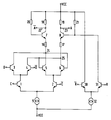
Das erfindungsgemäße Speicherelement enthält ein erstes Transistorpaar mit den Bipolartransistoren 1, 2, deren Emitter miteinander verbunden sind und über eine Stromquelle 9 mit einem Anschluß für ein erstes Versorgungspotential VEE verbunden sind. Mit den Kollektoren der Transistoren 1, 2 sind die gekoppelten Emitter jeweils eines weiteren Transistorpaares aus den Transistoren 3, 4 bzw. 5, 6 verbunden. Die Kollektoren der Transistoren der weiteren Transistorpaare sind paarweise gekoppelt. Wie in der Figur dargestellt, sind die Kollektoren der Transistoren 3, 5 zu einem Knoten 24 und die Kollektoren der Transistoren 4, 6 zu einem Knoten 25 verbunden. Die Knoten 24, 25 sind jeweils über die Reihenschaltung eines Widerstandes 16 bzw. 17 und die Kollektor-Emitter-Strecke eines Transistors 7 bzw. 8 mit einem Anschluß für ein zweites Versorgungspotential VCC verbunden. In den Kollektorkreis der Transistoren 7, 8 ist je ein Widerstand 18 bzw. 19 geschaltet. Die kollektorseitigen Anschlüsse der Widerstände 18, 19 weisen je einen Anschluß 22 bzw. 23 für ein Ausgangssignal ![]()
![]()
![]()
![]()
![]()
![]()
Als Einrichtung zum Rücksetzen des Speicherelementes ist ein Stromschalter aus Transistoren 30, 31 vorgesehen, deren gekoppelte Emitter über eine Stromquelle 32 mit dem Anschluß für das Versorgungspotential VEE verbunden sind. Der Kollektor des Transistors 30 ist mit dem Anschluß für das Versorgungspotential VCC verbunden, der Kollektor des Transistors 31 mit der Basis des Transistors 8. Die Basisanschlüsse der Transistoren 31, 30 werden von komplementären Rücksetz-Signalen R bzw. ![]()
![]()
Die Funktionsweise des Speicherelementes wird im folgenden erläutert. Während einer H-Phase des Taktsignals C ist der Transistor 1 leitend, der Transistor 2 gesperrt. Wenn das Datensignal D beispielsweise H ist, ist der Transistor 3 leitend, der Transistor 4 gesperrt. Der von der Stromquelle 9 eingeprägte Strom fließt dann über den Pfad der Transistoren 3, 1 und über den Pfad der Widerstände 16, 18 und des Transistors 7. Der Widerstand 18 ist derart dimensioniert, daß der Pegel des Ausgangssignals ![]()
![]()
![]()
![]()
![]()
![]()
Die Transistoren 7, 8 sind bezüglich des Versorgungspotentials VCC in Emitterfolgerschaltung geschaltet. Das Potential an den Emittern der Transistoren 7, 8 ist folglich konstant und setzt sich aus dem Spannungsabfall an den Widerständen 20 bzw. 21 und den Basis-Emitter-Spannungen der Transistoren 7 bzw. 8 zusammen. Durch die Transistoren 7, 8 werden die Signale A bzw. ![]()
![]()
Das Rücksetzsignal R sei vorerst L. Der Transistor 31 ist dann gesperrt, so daß das Basispotential des Transistors 8 dadurch unbeeinflußt ist und der Schaltzustand des Speicherelementes erhalten bleibt. Nun wird das Rücksetzsignal R auf H gesetzt. Der Transistor 31 ist leitend, der Transistor 30 gesperrt. Dadurch wird das Potential an der Basis des Transistors 8 abgesenkt, so daß - das Taktsignal C ist L - der Stromschalter der Transistoren 5, 6 umschaltet. Der Transistor 5 wird aufgrund seines nunmehr niedrigen Basispotentials gesperrt, der Transistor 6 leitet. Das Ausgangssignal A schaltet auf L um. Das Speicherelement wird also durch einen H-Pegel des Rücksetzsignals R rückgesetzt.The reset signal R is initially L. The
Um das Speicherelement mit einer Setzfunktion zu versehen, ist ein Stromschalter, entsprechend dem Stromschalter aus den Transistoren 30, 31 und der Stromquelle 32 notwendig, bei dem der Kollektoranschluß eines der Transistoren mit dem Basisanschluß des Transistors 7 verbunden ist. Wenn dieser Transistor leitend gesteuert ist, wird das Basispotential des Transistors 7 soweit abgesenkt, daß der Transistor 6 gesperrt und der Transistor 5 leitend ist. Das Ausgangssignal A ist dann H. Soll das Speicherelement eine Setz- und Rücksetzfunktion haben, ist je ein Stromschalter für die Setz- und Rücksetzfunktion notwendig. Diese Stromschalter werden entsprechend den obigen Ausführungen angeschlossen.In order to provide the memory element with a setting function, a current switch, corresponding to the current switch comprising the
Der erfindungsgemäße Stromschalter hat den Vorteil, daß die Knoten 24, 25 nicht zusätzlich kapazitiv belastet werden. Die für eine Setz- bzw. Rücksetzfunktion benötigten zusätzlichen Schaltungsmaßnahmen haben, wenn sie nicht aktiv sind, keinen Einfluß auf die Signalpfade im Speicherelement. Die Verzögerungszeit des Speicherelements und somit seine maximale Arbeitsgeschwindigkeit bleiben demnach unbeeinflußt.The current switch according to the invention has the advantage that the
Für ein erfindungsgemäßes Speicherelement sind weitere, nicht in der Zeichnung dargestellte Ausführungsformen möglich. Die Eingänge des in der Zeichnung dargestellten Speicherelements werden von komplementären Signalen gesteuert. In entsprechender Weise weisen die Ausgangssignalanschlüsse komplementäre Signale auf. Es ist auch möglich, nur einen der Arbeitswiderstände 18 oder 19 und nur einen der entsprechenden Ausgangssignalanschlüsse 22 bzw. 23 zu verwenden. Der Kollektor einer der Transistoren 7, 8 ist dann unmittelbar mit dem Anschluß für das Versorgungspotential VCC verbunden.Further embodiments, not shown in the drawing, are possible for a memory element according to the invention. The inputs of the memory element shown in the drawing are controlled by complementary signals. In a corresponding manner, the output signal connections have complementary signals. It is also possible to use only one of the
Weiterhin ist es möglich, als Referenzsignale für die Signale D, C, R anstelle der komplementären Signale ![]()
![]()
![]()
![]()
![]()
![]()
Es ist auch denkbar, die Basis nur eines der Transistoren 5, 6 mit dem Knoten 25 bzw. 24 zu verbinden. Die Basis des jeweils anderen der Transistoren 5, 6 wird dann von einem Referenzpotential gesteuert. Der Wert dieses Referenzpotentials liegt vorzugsweise in der Mitte des an der Basis des einen der Transistoren anliegenden Pegelhubs. Üblicherweise ist die Schaltung so dimensioniert, daß diese Pegel den Pegelwerten für L und H des Signals D entsprechen.It is also conceivable to connect the base of only one of the
Claims (5)
Applications Claiming Priority (2)
| Application Number | Priority Date | Filing Date | Title |
|---|---|---|---|
| DE4231178A DE4231178C2 (en) | 1992-09-17 | 1992-09-17 | Storage element |
| DE4231178 | 1992-09-17 |
Publications (3)
| Publication Number | Publication Date |
|---|---|
| EP0588111A2 true EP0588111A2 (en) | 1994-03-23 |
| EP0588111A3 EP0588111A3 (en) | 1995-06-07 |
| EP0588111B1 EP0588111B1 (en) | 1997-12-03 |
Family
ID=6468212
Family Applications (1)
| Application Number | Title | Priority Date | Filing Date |
|---|---|---|---|
| EP93113494A Expired - Lifetime EP0588111B1 (en) | 1992-09-17 | 1993-08-24 | Memory element |
Country Status (4)
| Country | Link |
|---|---|
| US (1) | US5349554A (en) |
| EP (1) | EP0588111B1 (en) |
| JP (1) | JP3461540B2 (en) |
| DE (2) | DE4231178C2 (en) |
Families Citing this family (3)
| Publication number | Priority date | Publication date | Assignee | Title |
|---|---|---|---|---|
| JPH09153593A (en) * | 1995-11-30 | 1997-06-10 | Nec Corp | Bimos logic circuit |
| US6798263B1 (en) * | 2002-11-25 | 2004-09-28 | Applied Micro Circuits Corporation | Reset feature for a low voltage differential latch |
| KR100995315B1 (en) | 2008-10-29 | 2010-11-19 | 주식회사 유니테스트 | High speed latch circuit and frequency divider having the same |
Citations (3)
| Publication number | Priority date | Publication date | Assignee | Title |
|---|---|---|---|---|
| US3801967A (en) * | 1971-12-30 | 1974-04-02 | Ibm | Monolithic bipolar transistor storage arrangement with latent bit pattern |
| EP0257938A2 (en) * | 1986-08-28 | 1988-03-02 | Advanced Micro Devices, Inc. | Digital memory with reset/preset capabilities |
| WO1991015855A1 (en) * | 1990-04-06 | 1991-10-17 | International Business Machines Corporation | Memory cell with active write load |
Family Cites Families (4)
| Publication number | Priority date | Publication date | Assignee | Title |
|---|---|---|---|---|
| US4506171A (en) * | 1982-12-29 | 1985-03-19 | Westinghouse Electric Corp. | Latching type comparator |
| US4599526A (en) * | 1983-05-13 | 1986-07-08 | At&T Bell Laboratories | Clocked latching circuit |
| JP2621311B2 (en) * | 1988-03-10 | 1997-06-18 | 日本電気株式会社 | Comparator with latch circuit |
| US5206550A (en) * | 1991-06-20 | 1993-04-27 | Texas Instruments, Incorporated | Amplifier with actively clamped load |
-
1992
- 1992-09-17 DE DE4231178A patent/DE4231178C2/en not_active Expired - Fee Related
-
1993
- 1993-08-24 EP EP93113494A patent/EP0588111B1/en not_active Expired - Lifetime
- 1993-08-24 DE DE59307771T patent/DE59307771D1/en not_active Expired - Fee Related
- 1993-09-13 JP JP25256793A patent/JP3461540B2/en not_active Expired - Fee Related
- 1993-09-17 US US08/123,524 patent/US5349554A/en not_active Expired - Lifetime
Patent Citations (3)
| Publication number | Priority date | Publication date | Assignee | Title |
|---|---|---|---|---|
| US3801967A (en) * | 1971-12-30 | 1974-04-02 | Ibm | Monolithic bipolar transistor storage arrangement with latent bit pattern |
| EP0257938A2 (en) * | 1986-08-28 | 1988-03-02 | Advanced Micro Devices, Inc. | Digital memory with reset/preset capabilities |
| WO1991015855A1 (en) * | 1990-04-06 | 1991-10-17 | International Business Machines Corporation | Memory cell with active write load |
Also Published As
| Publication number | Publication date |
|---|---|
| JPH06209237A (en) | 1994-07-26 |
| EP0588111A3 (en) | 1995-06-07 |
| DE4231178C2 (en) | 1994-07-21 |
| EP0588111B1 (en) | 1997-12-03 |
| DE4231178A1 (en) | 1994-03-24 |
| US5349554A (en) | 1994-09-20 |
| JP3461540B2 (en) | 2003-10-27 |
| DE59307771D1 (en) | 1998-01-15 |
Similar Documents
| Publication | Publication Date | Title |
|---|---|---|
| DE3523400C2 (en) | Circuit arrangement for a class AB output stage with a large oscillation range | |
| DE4236430C1 (en) | Switching stage using current switch technology | |
| DE2430126A1 (en) | HYBRID TRANSISTOR CIRCUIT | |
| EP0093996A1 (en) | Level conversion circuitry | |
| DE2828325A1 (en) | EMITTER COUPLED LOGIC STAGE | |
| DE2416534B2 (en) | TRANSISTOR CIRCUIT FOR REVERSING THE DIRECTION OF CURRENT IN A CONSUMER | |
| DE4010145C1 (en) | ||
| DE2925008A1 (en) | INTEGRATED POWER DRIVER CIRCUIT | |
| EP0583688A1 (en) | Digital current switch | |
| DE2314015B2 (en) | Signal amplifier | |
| EP0013710A1 (en) | Push-pull driver, the output of which may be directly connected to the outputs of other drivers | |
| EP0588111B1 (en) | Memory element | |
| DE19547754C1 (en) | Control circuit for BiCMOS bus driver | |
| DE4321483C2 (en) | Line driver switching stage in current switch technology | |
| EP0057239A1 (en) | Monolithic integrated push-pull driver circuit | |
| DE69630018T2 (en) | LOGICAL CIRCUIT FOR LOW VOLTAGES | |
| EP0735493A1 (en) | Bus driver circuit | |
| EP0421016A1 (en) | ECL-TTL signal level converter | |
| EP0610770B1 (en) | Multiplexing circuit arrangement using current switching | |
| DE3739872C2 (en) | ||
| DE3145771C2 (en) | ||
| DE2139328C3 (en) | Device for operating a capacitive load | |
| DE3311258C1 (en) | Circuit arrangement for monitoring an operating voltage | |
| EP0029480A1 (en) | Emitter follower logic circuit | |
| DE2246756B2 (en) | Electronic data storage |
Legal Events
| Date | Code | Title | Description |
|---|---|---|---|
| PUAI | Public reference made under article 153(3) epc to a published international application that has entered the european phase |
Free format text: ORIGINAL CODE: 0009012 |
|
| AK | Designated contracting states |
Kind code of ref document: A2 Designated state(s): DE FR GB IT |
|
| PUAL | Search report despatched |
Free format text: ORIGINAL CODE: 0009013 |
|
| AK | Designated contracting states |
Kind code of ref document: A3 Designated state(s): DE FR GB IT |
|
| 17P | Request for examination filed |
Effective date: 19951207 |
|
| GRAG | Despatch of communication of intention to grant |
Free format text: ORIGINAL CODE: EPIDOS AGRA |
|
| 17Q | First examination report despatched |
Effective date: 19970120 |
|
| GRAG | Despatch of communication of intention to grant |
Free format text: ORIGINAL CODE: EPIDOS AGRA |
|
| GRAH | Despatch of communication of intention to grant a patent |
Free format text: ORIGINAL CODE: EPIDOS IGRA |
|
| GRAH | Despatch of communication of intention to grant a patent |
Free format text: ORIGINAL CODE: EPIDOS IGRA |
|
| GRAA | (expected) grant |
Free format text: ORIGINAL CODE: 0009210 |
|
| AK | Designated contracting states |
Kind code of ref document: B1 Designated state(s): DE FR GB IT |
|
| REF | Corresponds to: |
Ref document number: 59307771 Country of ref document: DE Date of ref document: 19980115 |
|
| ET | Fr: translation filed | ||
| ITF | It: translation for a ep patent filed |
Owner name: STUDIO JAUMANN P. & C. S.N.C. |
|
| GBT | Gb: translation of ep patent filed (gb section 77(6)(a)/1977) |
Effective date: 19980205 |
|
| PLBE | No opposition filed within time limit |
Free format text: ORIGINAL CODE: 0009261 |
|
| STAA | Information on the status of an ep patent application or granted ep patent |
Free format text: STATUS: NO OPPOSITION FILED WITHIN TIME LIMIT |
|
| 26N | No opposition filed | ||
| PGFP | Annual fee paid to national office [announced via postgrant information from national office to epo] |
Ref country code: DE Payment date: 20011022 Year of fee payment: 9 |
|
| REG | Reference to a national code |
Ref country code: GB Ref legal event code: IF02 |
|
| PG25 | Lapsed in a contracting state [announced via postgrant information from national office to epo] |
Ref country code: DE Free format text: LAPSE BECAUSE OF NON-PAYMENT OF DUE FEES Effective date: 20030301 |
|
| PGFP | Annual fee paid to national office [announced via postgrant information from national office to epo] |
Ref country code: FR Payment date: 20030813 Year of fee payment: 11 |
|
| PG25 | Lapsed in a contracting state [announced via postgrant information from national office to epo] |
Ref country code: FR Free format text: LAPSE BECAUSE OF NON-PAYMENT OF DUE FEES Effective date: 20050429 |
|
| REG | Reference to a national code |
Ref country code: FR Ref legal event code: ST |
|
| PG25 | Lapsed in a contracting state [announced via postgrant information from national office to epo] |
Ref country code: IT Free format text: LAPSE BECAUSE OF NON-PAYMENT OF DUE FEES;WARNING: LAPSES OF ITALIAN PATENTS WITH EFFECTIVE DATE BEFORE 2007 MAY HAVE OCCURRED AT ANY TIME BEFORE 2007. THE CORRECT EFFECTIVE DATE MAY BE DIFFERENT FROM THE ONE RECORDED. Effective date: 20050824 |
|
| PGFP | Annual fee paid to national office [announced via postgrant information from national office to epo] |
Ref country code: GB Payment date: 20060824 Year of fee payment: 14 |
|
| GBPC | Gb: european patent ceased through non-payment of renewal fee |
Effective date: 20070824 |
|
| PG25 | Lapsed in a contracting state [announced via postgrant information from national office to epo] |
Ref country code: GB Free format text: LAPSE BECAUSE OF NON-PAYMENT OF DUE FEES Effective date: 20070824 |