EP0587404A2 - Elektronische Motorschutzvorrichtung - Google Patents
Elektronische Motorschutzvorrichtung Download PDFInfo
- Publication number
- EP0587404A2 EP0587404A2 EP93307044A EP93307044A EP0587404A2 EP 0587404 A2 EP0587404 A2 EP 0587404A2 EP 93307044 A EP93307044 A EP 93307044A EP 93307044 A EP93307044 A EP 93307044A EP 0587404 A2 EP0587404 A2 EP 0587404A2
- Authority
- EP
- European Patent Office
- Prior art keywords
- voltage
- output
- comparator
- inverting input
- protection system
- Prior art date
- Legal status (The legal status is an assumption and is not a legal conclusion. Google has not performed a legal analysis and makes no representation as to the accuracy of the status listed.)
- Granted
Links
Images


Classifications
-
- H—ELECTRICITY
- H02—GENERATION; CONVERSION OR DISTRIBUTION OF ELECTRIC POWER
- H02P—CONTROL OR REGULATION OF ELECTRIC MOTORS, ELECTRIC GENERATORS OR DYNAMO-ELECTRIC CONVERTERS; CONTROLLING TRANSFORMERS, REACTORS OR CHOKE COILS
- H02P1/00—Arrangements for starting electric motors or dynamo-electric converters
-
- H—ELECTRICITY
- H02—GENERATION; CONVERSION OR DISTRIBUTION OF ELECTRIC POWER
- H02H—EMERGENCY PROTECTIVE CIRCUIT ARRANGEMENTS
- H02H7/00—Emergency protective circuit arrangements specially adapted for specific types of electric machines or apparatus or for sectionalised protection of cable or line systems, and effecting automatic switching in the event of an undesired change from normal working conditions
- H02H7/08—Emergency protective circuit arrangements specially adapted for specific types of electric machines or apparatus or for sectionalised protection of cable or line systems, and effecting automatic switching in the event of an undesired change from normal working conditions for dynamo-electric motors
- H02H7/09—Emergency protective circuit arrangements specially adapted for specific types of electric machines or apparatus or for sectionalised protection of cable or line systems, and effecting automatic switching in the event of an undesired change from normal working conditions for dynamo-electric motors against over-voltage; against reduction of voltage; against phase interruption
-
- H—ELECTRICITY
- H02—GENERATION; CONVERSION OR DISTRIBUTION OF ELECTRIC POWER
- H02H—EMERGENCY PROTECTIVE CIRCUIT ARRANGEMENTS
- H02H1/00—Details of emergency protective circuit arrangements
- H02H1/06—Arrangements for supplying operative power
-
- H—ELECTRICITY
- H02—GENERATION; CONVERSION OR DISTRIBUTION OF ELECTRIC POWER
- H02H—EMERGENCY PROTECTIVE CIRCUIT ARRANGEMENTS
- H02H7/00—Emergency protective circuit arrangements specially adapted for specific types of electric machines or apparatus or for sectionalised protection of cable or line systems, and effecting automatic switching in the event of an undesired change from normal working conditions
- H02H7/08—Emergency protective circuit arrangements specially adapted for specific types of electric machines or apparatus or for sectionalised protection of cable or line systems, and effecting automatic switching in the event of an undesired change from normal working conditions for dynamo-electric motors
- H02H7/085—Emergency protective circuit arrangements specially adapted for specific types of electric machines or apparatus or for sectionalised protection of cable or line systems, and effecting automatic switching in the event of an undesired change from normal working conditions for dynamo-electric motors against excessive load
- H02H7/0852—Emergency protective circuit arrangements specially adapted for specific types of electric machines or apparatus or for sectionalised protection of cable or line systems, and effecting automatic switching in the event of an undesired change from normal working conditions for dynamo-electric motors against excessive load directly responsive to abnormal temperature by using a temperature sensor
-
- H—ELECTRICITY
- H02—GENERATION; CONVERSION OR DISTRIBUTION OF ELECTRIC POWER
- H02H—EMERGENCY PROTECTIVE CIRCUIT ARRANGEMENTS
- H02H11/00—Emergency protective circuit arrangements for preventing the switching-on in case an undesired electric working condition might result
- H02H11/006—Emergency protective circuit arrangements for preventing the switching-on in case an undesired electric working condition might result in case of too high or too low voltage
- H02H11/007—Emergency protective circuit arrangements for preventing the switching-on in case an undesired electric working condition might result in case of too high or too low voltage involving automatic switching for adapting the protected apparatus to the supply voltage
Definitions
- This invention relates generally to protection apparatus for electric motors and more specifically to electronic protection systems particularly suitable for compressor motors.
- thermo sensors such as positive temperature coefficient (PTC) of resistivity sensors
- PTC positive temperature coefficient
- the protection system has a power supply including a conventional transformer to convert outside supply voltage to a selected lower voltage suitable for operation of the control circuit.
- the control circuit utilizes a 24 volt supply so that separate transformer means, or at least a transformer with selected taps has to be utilized with different line voltage supplies. This results in having to provide different models of the protection system for different line voltage applications.
- a solid state power supply comprising an integrated circuit having a first switching pre-regulator section and a second voltage regulator section is used to provide a selected DC voltage.
- the switching pre-regulator conducts for a portion of the positive half of the AC line cycle which is used to charge a capacitor which in turn is coupled to the voltage regulator to provide a first level of DC voltage.
- the first level of DC voltage is used to directly drive a relay to control energization of the motor contactor.
- the first level of DC voltage is in turn stepped down by a limiting resistor and a zener diode to provide a second level of DC voltage for energizing the control circuitry.
- the control circuitry comprises a plurality of cascaded operational amplifiers in the form of comparator sections providing a single channel including an over-temperature protection section in which one or more PTC thermal sensors are coupled to the inverting input of a first comparator.
- the output of the first comparator is coupled to a buffer comparator which in turn is coupled to the base of a transistor serially connected to the relay coil.
- the output of the first comparator is also optionally connected to a time delay comparator whose output is coupled back to the inverting input of the first comparator.
- the output of the first comparator is also optionally coupled to the output of a low voltage comparator.
- the protection system is mounted on a circuit board received in the bottom half of a housing which is encased with potting material to provide vibration insensitivity, environment protection and to meet agency standard spacing requirements.
- the top half of the housing has a plurality of ribbed depending skirts adapted to extend into the potting material to lock the housing parts together.
- the input blade line terminals of the system are configured smaller than the sensor or output terminals to obviate any possibility of miswiring by putting line voltage across the control circuit or sensor circuits.
- protection apparatus 10 made in accordance with the invention comprises a power supply section 12, over-temperature protection section 14, output circuit 18, time delay section 20 and low voltage cut-out section 22.
- Each of sections 14, 16, 20 and 22 includes an operational amplifier comparators 1, 4, 2 and 3 respectively each having an output BJT transistor (open collector).
- comparators 1, 4, 2 and 3 respectively each having an output BJT transistor (open collector).
- the output transistor of comparator 1 is off, the output transistor of comparator 4 and 2 are on, and the output transistor of comparator 3 is off.
- an over-temperature condition occurs it will cause the output transistor of comparator 1 to turn on and the output transistor of comparators 4 and 2 to turn off (comparator 3 still being off).
- When low voltage conditions occur the output transistor of comparators 1, 4 and 2 are off and the output transistor of comparator 3 turns on.
- power supply section 12 comprises a fuse F1 connected to the AC high, terminal T2 as a safety feature so that in the event of a short circuit the apparatus will fail with an open circuit.
- a surge suppressor varistor MOV1 is coupled across the AC high terminal T2 and AC return terminal T1 to clamp high frequency and high energy transients such as lightning surges.
- Resistors R1, R2 and capacitor C1 connected across the AC lines serve as a low pass filter to filter high frequency noise and line spikes. Additionally, resistors R1, R2 serve as current limiting devices for the SCR based pre-regulator to be discussed below.
- Circuit section 10 includes a single chip power supply, integrated circuit 24, an eight pin device having a first switching pre-regulator section and a second voltage regulator section.
- Pin 8 connected to the pre-regulator section, is connected to the AC high line through resistors R1, R2.
- Pin 1 is connected to the AC return line and through an inhibit capacitor C3 to pin 4 to provide protection from transients that exceed the dv/dt rating of IC 24 by going from a high impedance to a low impedance thereby preventing an internal SCR in IC 24 from gating on.
- An energy storage capacitor C2 is connected between pin 2 through charging resistor R3 and pin 1.
- Pin 2 is coupled internally of chip 24 to the output of the switching pre-regulator section and the input of the voltage regulator section.
- the output of the voltage regulator section is connected to pin 6 with a feedback resistor R4 connected between pins 6 and 5.
- Pin 3 is connected to the analog ground of the control and output circuit.
- the output of the regulator section provides a 24 volt DC supply on line 28 for relay coil K1 and associated contacts M1, M2.
- Fig 2 which shows the voltage vs time curve at a of line voltage, typically 60 Hertz frequency and at b the waveform as seen at pin 8 with the SCR conduction of the pre-regulator section typically in the order of 1 millisecond for a 60 Hertz frequency occurring on the positive half of the AC cycle.
- a lower voltage i.e., 12 volts, suitable for operation of the control circuit, to be explained infra, is provided by suitable means such as a dropping resistor R28 serially connected to a 12 volt zener diode ZD1 connected between the output of IC 24 and ground.
- Power supply section 12 also includes a snubber capacitor C4 connected between the low voltage output at the junction of resistor R28 and diode ZD1 and ground.
- the low voltage power supply could be provided by a voltage divider comprising two resistors, if desired.
- Over-temperature protection section 14 comprises a comparator 1 having its inverting input connected, through diode D1, resistor R29 and capacitor C9 to the junction of a reference resistor R5 and a PTC resistor which are connected between control circuit supply voltage 28 and ground.
- Diode D1 serves to isolate resistor R5 and the PTC from any feedback from the supply rail 28 through resistors R16, R17 when the output transistor of comparator 2 is off and the inverting input is tied to the 12 volt rail.
- the non-inverting input of the comparator 1 is connected to the junction of voltage divider resistors R6, R7 connected between line 28 and ground to establish a reference voltage.
- Feedback resistor R8 is connected between the output of comparator 1 and the non-inverting input.
- Capacitor C9 is connected between the inverting output of comparator 1 and ground.
- the RC network of resistor R29 and capacitor C9 snubs down noise transients on the sensor input thereby preventing nuisance tripping
- comparator 1 is connected to the junction of a voltage divider in buffer circuit portion 16 comprising resistors R9, R10 and the junction in turn is connected to the inverting input of comparator 4.
- the non-inverting input is connected to the junction of a voltage divider comprising resistors R11, R 12.
- Feedback resistor R13 providing hysteresis which in turn provides a clear demarcation for switching of comparator 4 and avoiding contact chatter is connected between the output of comparator 4 and the non-inverting input.
- the output of comparator 4 is connected to the output voltage line 26 of IC 24 through resistors R14, R15 in output circuit 18.
- PNP transistor Q1 The emitter, collector terminals of PNP transistor Q1 are serially connected between supply line 26 and relay coil K1 which in turn is connected to ground.
- the base of the transistor is connected to the junction of resistors R14, R15.
- Diode D3 is coupled across relay coil K1 to prevent back EMF, thereby protecting transistor Q1.
- a fixed voltage reference provided by voltage divider R6, R7 establishes a threshold level at the non-inverting input of comparator 1.
- the variable voltage provided by the PTC sensor comprises the variable voltage at the inverting terminal of comparator 1 which varies according to the change in the resistance of the PTC dependent on changes in temperature of the PTC. When the voltage at the inverting terminal exceeds that of the non-inverting terminal the output NPN transistor of comparator 1 is biased on thereby sinking current to ground.
- Time delay section 20 is an optional feature comprising comparator 2 whose non-inverting input is connected through resistor R21 to a point between resistor R19 and diode D4 to the junction of resistors R18 and R20.
- Resistor R18 is connected to the supply rail 28 while resistor R20 is connected to the output of comparator 1.
- the inverting input of comparator 2 is connected to the junction of resistors R18 and R20.
- the RC network comprising capacitor C6 coupled around resistor R19 provides the selected time delay.
- a resistance value of 1.1 MEG. ohms for resistor R19 provides a four minute delay using 100 uf for capacitor C6. By using a resistance value of 500K ohms for R19 a two minute delay is provided.
- Resistor R21 prevents discharge current from capacitor C6 from going back into the non-inverting terminal.
- the output of comparator 2 is connected to the junction of resistors R16, R17 which are connected between supply line 28 and the inverting input of comparator 1. During steady state operation of a motor the input voltage at the inverting terminal of comparator 2 exceeds that of the non-inverting terminal due to the voltage drop of diode D4 with the output transistor biased on.
- the output transistor of comparator 1 When the module trips due to an over-temperature condition, or the like, the output transistor of comparator 1 is biased on sinking current from resistor R20 to ground thereby lowering potential between voltage divider R18, R20 so that voltage at non-inverting terminal of comparator 2 exceeds that of the inverting terminal and the output transistor of comparator 2 is biased off. Since the output of comparator 2 is tied to the inverting input of comparator 1 it keeps the inverting input of comparator 1 tied to the supply rail 26 until capacitor C6, discharging through resistor R19, decreases to a value lower than the voltage at the inverting input of comparator 2 and the circuit is then reset. Diode D4 prevents any current from capacitor C6 back feeding to the supply rail.
- Low voltage cut-out circuit section 22 is another optional feature and it comprises comparator 3 whose non-inverting input terminal is connected to the junction of resistors R25, R26 which are connected through diode D6 and resistor R27 between AC line voltage and ground with capacitor C8 coupled across resistors R25, R26.
- the inverting input terminal of comparator 3 is connected between resistor R23 and zener diode ZD2 connected between supply line 28 and ground to provide a reference voltage.
- the output of comparator 3 is connected to the output of comparator 1.
- Feedback resistor R22 and diode D5 are connected between the output of comparator 3 and the non-inverting input thereof. Resistor R22 provides hysteresis to avoid problems with the ripple voltage associated with charging of capacitor C8.
- resistor R22 and diode D5 are in parallel with resistor R26; however, once the peak of the ripple voltage charging capacitor C8 exceeds the reference voltage of zener diode ZD2 causing a change of state of comparator 3 resistor R22 is effectively removed with the voltage at the non-inverting input of comparator 3 going significantly higher, e.g., from approximately 3.2V to approximately 5V.
- Capacitor C7 is connected between the input terminals of comparator 3 to suppress any high frequency transients at the input terminals.
- the output transistor of comparator 3 is off and the potential of the inverting input of comparator 3 is less than the potential at the non-inverting input.
- line voltage starts to decrease thereby decreasing the voltage at the non-inverting terminal below the preselected level thereby biasing the output transistor of comparator 3 on.
- Current flows from supply rail 28 and since the output transistor of comparator 1 is off the current flows to ground through output transistor of comparator 3.
- the inverting input of comparator 4 is than tied to ground making the positive or non-inverting input higher than the negative input turning off the output transistor of comparator 4, so that the base junction of transistor Q1 is no longer tied to ground.
- time delay option When the time delay option is used if an over-temperature or low voltage condition is sensed a pre-programmed two or four minute delay will be activated preventing energization of the relay (and motor) even though the PTC sensor may have cooled to the reset temperature.
- the time delay function is used whenever the low voltage function is used to prevent undesirable oscillation should the voltage hover near the designed cut-out value.
- the time delay function can easily be shorted out using appropriate jumpers to tie the inputs of comparators 2 and 3 to ground and removing jumpers J1 and J2.
- a circuit built in accordance with the invention has the following component values:
- the circuit components of Fig. 1 mounted on a suitable circuit board are received in the bottom housing half 30 having upstanding wall 32 infilled with a suitable electrically insulative but thermally conductive potting material such as two part epoxy (2850FTFR with catalyst LN2636-101) available from Emerson and Cuming Inc.
- a suitable electrically insulative but thermally conductive potting material such as two part epoxy (2850FTFR with catalyst LN2636-101) available from Emerson and Cuming Inc.
- a suitable electrically insulative but thermally conductive potting material such as two part epoxy (2850FTFR with catalyst LN2636-101) available from Emerson and Cuming Inc.
- 2850FTFR with catalyst LN2636-101 two part epoxy
- Terminals T2, T1, M2, M1 and S2, S1 project upwardly from the epoxy and are received through terminal apertures in housing half 34.
- terminal block members T2, T1 are smaller than the remaining terminals in order to ensure that line power will not be connected to the output or sensor terminals. This obviates potential miswiring by field personnel or the like which otherwise could result in damaging the control circuit.
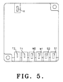
- Terminal X shown in Figs. 1, 3 and 5 is used to disable the time delay feature connecting point X with S1 so that other features of the circuit can be tested more expeditiously.
- the over-temperature protection system enables the over-temperature protection system to be used with a wide range of line voltages, from 30 to 264 V rms without any change in the systems components or in the way that the system is connected to line voltage.
- the over-temperature protection portion of the system can readily be used with 120 or 240 VAC applications. Additional advantages are obtained since the transformer, along with the diode rectifier network of the prior art, is replaced by the IC 24 thereby resulting in a reduction in size and weight of the system. Cost reduction is also achieved by replacing a conventional triac and its accessories with a low cost relay.
- the protection system built in accordance with the invention is not only less expensive due to the elimination of the transformer and reduction of inventory parts it is more reliable and is easily manufactured.
- the protection system is particularly suitable for use with refrigerant compressor motors to provide protection from overheating due to locked rotor, running overload, light loads, loss of charge and high discharge gas temperature conditions.
- the system can be provided with or without the low voltage cut-out and time delay features.
Landscapes
- Engineering & Computer Science (AREA)
- Power Engineering (AREA)
- Protection Of Generators And Motors (AREA)
- Emergency Protection Circuit Devices (AREA)
- Control Of Ac Motors In General (AREA)
Applications Claiming Priority (2)
| Application Number | Priority Date | Filing Date | Title |
|---|---|---|---|
| US94325492A | 1992-09-10 | 1992-09-10 | |
| US943254 | 1992-09-10 |
Publications (3)
| Publication Number | Publication Date |
|---|---|
| EP0587404A2 true EP0587404A2 (de) | 1994-03-16 |
| EP0587404A3 EP0587404A3 (de) | 1994-05-18 |
| EP0587404B1 EP0587404B1 (de) | 1997-01-22 |
Family
ID=25479321
Family Applications (1)
| Application Number | Title | Priority Date | Filing Date |
|---|---|---|---|
| EP93307044A Expired - Lifetime EP0587404B1 (de) | 1992-09-10 | 1993-09-07 | Elektronische Motorschutzvorrichtung |
Country Status (5)
| Country | Link |
|---|---|
| US (1) | US5585990A (de) |
| EP (1) | EP0587404B1 (de) |
| JP (1) | JPH06197444A (de) |
| KR (1) | KR100283069B1 (de) |
| DE (1) | DE69307635T2 (de) |
Cited By (1)
| Publication number | Priority date | Publication date | Assignee | Title |
|---|---|---|---|---|
| CN103760782A (zh) * | 2013-12-31 | 2014-04-30 | 山西汾西机电有限公司 | 煤矿井下矿用隔爆兼本质安全型冷却干燥机控制电路 |
Families Citing this family (11)
| Publication number | Priority date | Publication date | Assignee | Title |
|---|---|---|---|---|
| US5784232A (en) * | 1997-06-03 | 1998-07-21 | Tecumseh Products Company | Multiple winding sensing control and protection circuit for electric motors |
| GB9721091D0 (en) * | 1997-10-03 | 1997-12-03 | Arctic Circle Limited | A terminal box for a refrigeration compressor |
| US6072397A (en) * | 1998-12-03 | 2000-06-06 | Ascend Communications, Inc. | Method and apparatus for reducing flame emissions from an electronics enclosure |
| US6169648B1 (en) * | 1999-04-09 | 2001-01-02 | Texas Instruments Incorporated | Electronic motor protection system |
| US6288876B1 (en) | 1999-04-16 | 2001-09-11 | International Business Machines Corporation | Melting and refreezing method for smothing and load/unloading lift tab for disk drive smoothed lift tab and gimbal assembly and data storage device incorporating smoothed lift tab |
| US7099140B2 (en) * | 2002-11-07 | 2006-08-29 | General Electric Company | Method and apparatus for combining PTCR/OL and run capacitor |
| TWM243837U (en) * | 2003-02-24 | 2004-09-11 | Sunonwealth Electr Mach Ind Co | Over-heat protection circuit for a brushless DC motor |
| EP1932232A1 (de) * | 2005-10-07 | 2008-06-18 | Lg Electronics Inc. | Kompressor des stromsparenden typs und kühlschrank damit und verfahren zu seiner steuerung |
| CN101212133B (zh) * | 2007-12-21 | 2011-04-13 | 王卫东 | 带储能撞击装置的塑壳式机电一体化三相交流电动机保护器 |
| CN102621911A (zh) * | 2012-05-08 | 2012-08-01 | 江西电力职业技术学院 | 空调来电自启动控制器 |
| US10124871B1 (en) | 2017-08-31 | 2018-11-13 | Brunswick Corporation | Shift systems that facilitate resilient mounting of an outboard motor with respect to a marine vessel |
Family Cites Families (7)
| Publication number | Priority date | Publication date | Assignee | Title |
|---|---|---|---|---|
| US4281358A (en) * | 1978-09-01 | 1981-07-28 | Texas Instruments Incorporated | Multifunction dynamoelectric protection system |
| US4539618A (en) * | 1982-04-05 | 1985-09-03 | Siemens-Allis, Inc. | Digitally controlled overload relay |
| US4456871A (en) * | 1982-04-05 | 1984-06-26 | Siemens-Allis, Inc. | Power supply for electronic control system |
| US4636920A (en) * | 1985-09-05 | 1987-01-13 | Caterpillar Inc. | Printed circuit board mounting apparatus |
| US4851609A (en) * | 1988-05-10 | 1989-07-25 | Prabhakara Reddy | Protective housing for an electrical device |
| US5206572A (en) * | 1988-06-22 | 1993-04-27 | Siemens Energy & Automation, Inc. | Motor controller |
| US5170327A (en) * | 1990-11-05 | 1992-12-08 | Adc Telecommunications, Inc. | Distal distribution frame module |
-
1993
- 1993-09-07 EP EP93307044A patent/EP0587404B1/de not_active Expired - Lifetime
- 1993-09-07 DE DE69307635T patent/DE69307635T2/de not_active Expired - Fee Related
- 1993-09-08 KR KR1019930017973A patent/KR100283069B1/ko not_active Expired - Fee Related
- 1993-09-09 JP JP5224668A patent/JPH06197444A/ja active Pending
-
1995
- 1995-05-19 US US08/444,446 patent/US5585990A/en not_active Expired - Fee Related
Cited By (2)
| Publication number | Priority date | Publication date | Assignee | Title |
|---|---|---|---|---|
| CN103760782A (zh) * | 2013-12-31 | 2014-04-30 | 山西汾西机电有限公司 | 煤矿井下矿用隔爆兼本质安全型冷却干燥机控制电路 |
| CN103760782B (zh) * | 2013-12-31 | 2016-08-17 | 山西汾西机电有限公司 | 煤矿井下矿用隔爆兼本质安全型冷却干燥机控制电路 |
Also Published As
| Publication number | Publication date |
|---|---|
| KR940008220A (ko) | 1994-04-29 |
| US5585990A (en) | 1996-12-17 |
| KR100283069B1 (ko) | 2001-04-02 |
| DE69307635D1 (de) | 1997-03-06 |
| EP0587404B1 (de) | 1997-01-22 |
| EP0587404A3 (de) | 1994-05-18 |
| JPH06197444A (ja) | 1994-07-15 |
| DE69307635T2 (de) | 1997-05-15 |
Similar Documents
| Publication | Publication Date | Title |
|---|---|---|
| US5548464A (en) | Electronic motor protection apparatus | |
| EP0587404B1 (de) | Elektronische Motorschutzvorrichtung | |
| US5570258A (en) | Phase monitor and protection apparatus | |
| EP0792007B1 (de) | Universeller Leistungsmodul | |
| US5600550A (en) | Power converter for recreational vehicles and the like | |
| US4097789A (en) | Rotation-supervised d-c fan or blower system | |
| US6229682B1 (en) | Transient voltage surge suppressor | |
| WO1992008266A1 (en) | Line voltage monitor and controller with low voltage stabilization | |
| US20040105664A1 (en) | Linear electric motor controller and system for providing linear speed control | |
| JPS58108967A (ja) | スイツチングレギユレ−タ | |
| US6560086B2 (en) | Transient voltage surge suppressor | |
| EP0661789A2 (de) | Phasenfolgeverdrahtungsschutz | |
| US11811220B2 (en) | Soft starter for high-current electric devices | |
| US5675464A (en) | Stall or reduced-speed protection system for electric motor | |
| US6169648B1 (en) | Electronic motor protection system | |
| US20060120007A1 (en) | Apparatus for controlling interconnect switch | |
| JPH0315440B2 (de) | ||
| US5460221A (en) | Fan coil thermostat with circuitry to assure minimum power for relay pull-in | |
| JPS6273313A (ja) | 温度調節器用電流制限回路 | |
| US6522106B2 (en) | Automatic voltage regulating system for engine generator | |
| JPH0824605B2 (ja) | ヘアードライヤ | |
| US2731587A (en) | Motor protective system | |
| CN1334984B (zh) | 电流限制装置 | |
| US4768125A (en) | Protective device for an electric motor | |
| GB2117196A (en) | Detecting faults in a multi phase AC supply |
Legal Events
| Date | Code | Title | Description |
|---|---|---|---|
| PUAI | Public reference made under article 153(3) epc to a published international application that has entered the european phase |
Free format text: ORIGINAL CODE: 0009012 |
|
| AK | Designated contracting states |
Kind code of ref document: A2 Designated state(s): DE FR GB IT NL |
|
| PUAL | Search report despatched |
Free format text: ORIGINAL CODE: 0009013 |
|
| AK | Designated contracting states |
Kind code of ref document: A3 Designated state(s): DE FR GB IT NL |
|
| 17P | Request for examination filed |
Effective date: 19940808 |
|
| 17Q | First examination report despatched |
Effective date: 19950828 |
|
| GRAG | Despatch of communication of intention to grant |
Free format text: ORIGINAL CODE: EPIDOS AGRA |
|
| GRAH | Despatch of communication of intention to grant a patent |
Free format text: ORIGINAL CODE: EPIDOS IGRA |
|
| GRAH | Despatch of communication of intention to grant a patent |
Free format text: ORIGINAL CODE: EPIDOS IGRA |
|
| ITF | It: translation for a ep patent filed | ||
| GRAA | (expected) grant |
Free format text: ORIGINAL CODE: 0009210 |
|
| AK | Designated contracting states |
Kind code of ref document: B1 Designated state(s): DE FR GB IT NL |
|
| PG25 | Lapsed in a contracting state [announced via postgrant information from national office to epo] |
Ref country code: NL Free format text: LAPSE BECAUSE OF FAILURE TO SUBMIT A TRANSLATION OF THE DESCRIPTION OR TO PAY THE FEE WITHIN THE PRESCRIBED TIME-LIMIT Effective date: 19970122 |
|
| REF | Corresponds to: |
Ref document number: 69307635 Country of ref document: DE Date of ref document: 19970306 |
|
| ET | Fr: translation filed | ||
| NLV1 | Nl: lapsed or annulled due to failure to fulfill the requirements of art. 29p and 29m of the patents act | ||
| PLBE | No opposition filed within time limit |
Free format text: ORIGINAL CODE: 0009261 |
|
| STAA | Information on the status of an ep patent application or granted ep patent |
Free format text: STATUS: NO OPPOSITION FILED WITHIN TIME LIMIT |
|
| 26N | No opposition filed | ||
| REG | Reference to a national code |
Ref country code: GB Ref legal event code: IF02 |
|
| PGFP | Annual fee paid to national office [announced via postgrant information from national office to epo] |
Ref country code: GB Payment date: 20020808 Year of fee payment: 10 |
|
| PGFP | Annual fee paid to national office [announced via postgrant information from national office to epo] |
Ref country code: FR Payment date: 20020903 Year of fee payment: 10 |
|
| PGFP | Annual fee paid to national office [announced via postgrant information from national office to epo] |
Ref country code: DE Payment date: 20020930 Year of fee payment: 10 |
|
| PG25 | Lapsed in a contracting state [announced via postgrant information from national office to epo] |
Ref country code: GB Free format text: LAPSE BECAUSE OF NON-PAYMENT OF DUE FEES Effective date: 20030907 |
|
| PG25 | Lapsed in a contracting state [announced via postgrant information from national office to epo] |
Ref country code: DE Free format text: LAPSE BECAUSE OF NON-PAYMENT OF DUE FEES Effective date: 20040401 |
|
| GBPC | Gb: european patent ceased through non-payment of renewal fee |
Effective date: 20030907 |
|
| PG25 | Lapsed in a contracting state [announced via postgrant information from national office to epo] |
Ref country code: FR Free format text: LAPSE BECAUSE OF NON-PAYMENT OF DUE FEES Effective date: 20040528 |
|
| REG | Reference to a national code |
Ref country code: FR Ref legal event code: ST |
|
| PG25 | Lapsed in a contracting state [announced via postgrant information from national office to epo] |
Ref country code: IT Free format text: LAPSE BECAUSE OF NON-PAYMENT OF DUE FEES Effective date: 20050907 |