EP0585466A1 - Method and circuit for driving liquid crystal elements, and display apparatus - Google Patents
Method and circuit for driving liquid crystal elements, and display apparatus Download PDFInfo
- Publication number
- EP0585466A1 EP0585466A1 EP93905616A EP93905616A EP0585466A1 EP 0585466 A1 EP0585466 A1 EP 0585466A1 EP 93905616 A EP93905616 A EP 93905616A EP 93905616 A EP93905616 A EP 93905616A EP 0585466 A1 EP0585466 A1 EP 0585466A1
- Authority
- EP
- European Patent Office
- Prior art keywords
- row
- voltage
- column
- electrode
- electrodes
- Prior art date
- Legal status (The legal status is an assumption and is not a legal conclusion. Google has not performed a legal analysis and makes no representation as to the accuracy of the status listed.)
- Granted
Links
Images












Classifications
-
- G—PHYSICS
- G09—EDUCATION; CRYPTOGRAPHY; DISPLAY; ADVERTISING; SEALS
- G09G—ARRANGEMENTS OR CIRCUITS FOR CONTROL OF INDICATING DEVICES USING STATIC MEANS TO PRESENT VARIABLE INFORMATION
- G09G3/00—Control arrangements or circuits, of interest only in connection with visual indicators other than cathode-ray tubes
- G09G3/20—Control arrangements or circuits, of interest only in connection with visual indicators other than cathode-ray tubes for presentation of an assembly of a number of characters, e.g. a page, by composing the assembly by combination of individual elements arranged in a matrix no fixed position being assigned to or needed to be assigned to the individual characters or partial characters
- G09G3/34—Control arrangements or circuits, of interest only in connection with visual indicators other than cathode-ray tubes for presentation of an assembly of a number of characters, e.g. a page, by composing the assembly by combination of individual elements arranged in a matrix no fixed position being assigned to or needed to be assigned to the individual characters or partial characters by control of light from an independent source
- G09G3/36—Control arrangements or circuits, of interest only in connection with visual indicators other than cathode-ray tubes for presentation of an assembly of a number of characters, e.g. a page, by composing the assembly by combination of individual elements arranged in a matrix no fixed position being assigned to or needed to be assigned to the individual characters or partial characters by control of light from an independent source using liquid crystals
- G09G3/3611—Control of matrices with row and column drivers
- G09G3/3674—Details of drivers for scan electrodes
- G09G3/3681—Details of drivers for scan electrodes suitable for passive matrices only
-
- G—PHYSICS
- G09—EDUCATION; CRYPTOGRAPHY; DISPLAY; ADVERTISING; SEALS
- G09G—ARRANGEMENTS OR CIRCUITS FOR CONTROL OF INDICATING DEVICES USING STATIC MEANS TO PRESENT VARIABLE INFORMATION
- G09G3/00—Control arrangements or circuits, of interest only in connection with visual indicators other than cathode-ray tubes
- G09G3/20—Control arrangements or circuits, of interest only in connection with visual indicators other than cathode-ray tubes for presentation of an assembly of a number of characters, e.g. a page, by composing the assembly by combination of individual elements arranged in a matrix no fixed position being assigned to or needed to be assigned to the individual characters or partial characters
- G09G3/34—Control arrangements or circuits, of interest only in connection with visual indicators other than cathode-ray tubes for presentation of an assembly of a number of characters, e.g. a page, by composing the assembly by combination of individual elements arranged in a matrix no fixed position being assigned to or needed to be assigned to the individual characters or partial characters by control of light from an independent source
- G09G3/36—Control arrangements or circuits, of interest only in connection with visual indicators other than cathode-ray tubes for presentation of an assembly of a number of characters, e.g. a page, by composing the assembly by combination of individual elements arranged in a matrix no fixed position being assigned to or needed to be assigned to the individual characters or partial characters by control of light from an independent source using liquid crystals
- G09G3/3611—Control of matrices with row and column drivers
- G09G3/3622—Control of matrices with row and column drivers using a passive matrix
-
- G—PHYSICS
- G09—EDUCATION; CRYPTOGRAPHY; DISPLAY; ADVERTISING; SEALS
- G09G—ARRANGEMENTS OR CIRCUITS FOR CONTROL OF INDICATING DEVICES USING STATIC MEANS TO PRESENT VARIABLE INFORMATION
- G09G3/00—Control arrangements or circuits, of interest only in connection with visual indicators other than cathode-ray tubes
- G09G3/20—Control arrangements or circuits, of interest only in connection with visual indicators other than cathode-ray tubes for presentation of an assembly of a number of characters, e.g. a page, by composing the assembly by combination of individual elements arranged in a matrix no fixed position being assigned to or needed to be assigned to the individual characters or partial characters
- G09G3/34—Control arrangements or circuits, of interest only in connection with visual indicators other than cathode-ray tubes for presentation of an assembly of a number of characters, e.g. a page, by composing the assembly by combination of individual elements arranged in a matrix no fixed position being assigned to or needed to be assigned to the individual characters or partial characters by control of light from an independent source
- G09G3/36—Control arrangements or circuits, of interest only in connection with visual indicators other than cathode-ray tubes for presentation of an assembly of a number of characters, e.g. a page, by composing the assembly by combination of individual elements arranged in a matrix no fixed position being assigned to or needed to be assigned to the individual characters or partial characters by control of light from an independent source using liquid crystals
- G09G3/3611—Control of matrices with row and column drivers
- G09G3/3622—Control of matrices with row and column drivers using a passive matrix
- G09G3/3625—Control of matrices with row and column drivers using a passive matrix using active addressing
-
- G—PHYSICS
- G09—EDUCATION; CRYPTOGRAPHY; DISPLAY; ADVERTISING; SEALS
- G09G—ARRANGEMENTS OR CIRCUITS FOR CONTROL OF INDICATING DEVICES USING STATIC MEANS TO PRESENT VARIABLE INFORMATION
- G09G2310/00—Command of the display device
- G09G2310/02—Addressing, scanning or driving the display screen or processing steps related thereto
- G09G2310/0202—Addressing of scan or signal lines
- G09G2310/0205—Simultaneous scanning of several lines in flat panels
-
- G—PHYSICS
- G09—EDUCATION; CRYPTOGRAPHY; DISPLAY; ADVERTISING; SEALS
- G09G—ARRANGEMENTS OR CIRCUITS FOR CONTROL OF INDICATING DEVICES USING STATIC MEANS TO PRESENT VARIABLE INFORMATION
- G09G3/00—Control arrangements or circuits, of interest only in connection with visual indicators other than cathode-ray tubes
- G09G3/20—Control arrangements or circuits, of interest only in connection with visual indicators other than cathode-ray tubes for presentation of an assembly of a number of characters, e.g. a page, by composing the assembly by combination of individual elements arranged in a matrix no fixed position being assigned to or needed to be assigned to the individual characters or partial characters
- G09G3/2007—Display of intermediate tones
- G09G3/2011—Display of intermediate tones by amplitude modulation
-
- G—PHYSICS
- G09—EDUCATION; CRYPTOGRAPHY; DISPLAY; ADVERTISING; SEALS
- G09G—ARRANGEMENTS OR CIRCUITS FOR CONTROL OF INDICATING DEVICES USING STATIC MEANS TO PRESENT VARIABLE INFORMATION
- G09G3/00—Control arrangements or circuits, of interest only in connection with visual indicators other than cathode-ray tubes
- G09G3/20—Control arrangements or circuits, of interest only in connection with visual indicators other than cathode-ray tubes for presentation of an assembly of a number of characters, e.g. a page, by composing the assembly by combination of individual elements arranged in a matrix no fixed position being assigned to or needed to be assigned to the individual characters or partial characters
- G09G3/2007—Display of intermediate tones
- G09G3/2014—Display of intermediate tones by modulation of the duration of a single pulse during which the logic level remains constant
-
- G—PHYSICS
- G09—EDUCATION; CRYPTOGRAPHY; DISPLAY; ADVERTISING; SEALS
- G09G—ARRANGEMENTS OR CIRCUITS FOR CONTROL OF INDICATING DEVICES USING STATIC MEANS TO PRESENT VARIABLE INFORMATION
- G09G3/00—Control arrangements or circuits, of interest only in connection with visual indicators other than cathode-ray tubes
- G09G3/20—Control arrangements or circuits, of interest only in connection with visual indicators other than cathode-ray tubes for presentation of an assembly of a number of characters, e.g. a page, by composing the assembly by combination of individual elements arranged in a matrix no fixed position being assigned to or needed to be assigned to the individual characters or partial characters
- G09G3/2007—Display of intermediate tones
- G09G3/2018—Display of intermediate tones by time modulation using two or more time intervals
-
- G—PHYSICS
- G09—EDUCATION; CRYPTOGRAPHY; DISPLAY; ADVERTISING; SEALS
- G09G—ARRANGEMENTS OR CIRCUITS FOR CONTROL OF INDICATING DEVICES USING STATIC MEANS TO PRESENT VARIABLE INFORMATION
- G09G3/00—Control arrangements or circuits, of interest only in connection with visual indicators other than cathode-ray tubes
- G09G3/20—Control arrangements or circuits, of interest only in connection with visual indicators other than cathode-ray tubes for presentation of an assembly of a number of characters, e.g. a page, by composing the assembly by combination of individual elements arranged in a matrix no fixed position being assigned to or needed to be assigned to the individual characters or partial characters
- G09G3/34—Control arrangements or circuits, of interest only in connection with visual indicators other than cathode-ray tubes for presentation of an assembly of a number of characters, e.g. a page, by composing the assembly by combination of individual elements arranged in a matrix no fixed position being assigned to or needed to be assigned to the individual characters or partial characters by control of light from an independent source
- G09G3/36—Control arrangements or circuits, of interest only in connection with visual indicators other than cathode-ray tubes for presentation of an assembly of a number of characters, e.g. a page, by composing the assembly by combination of individual elements arranged in a matrix no fixed position being assigned to or needed to be assigned to the individual characters or partial characters by control of light from an independent source using liquid crystals
- G09G3/3611—Control of matrices with row and column drivers
Definitions
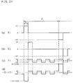
- Fig. 21 shows a drawing of applied voltage waveforms that illustrate one example of the prior art driving method of multiplex driving a simple matrix type liquid crystal cell such as that shown in Fig. 22, which operates according to the amplitude selective addressing scheme.
- Figs. 21 (a) and 21 (b) show the voltage waveforms that will be applied to row electrodes X1 and X2, respectively.
- Fig. 21 (c) shows the waveform to be applied to column electrode Y1.
- Fig. 21 (d) shows the voltage waveform that will be applied to the pixel defined by the column electrode Y1 and the row electrode X1.
- driving is performed by applying the row voltage to one line each of row electrodes X1, X2 .... X n selected in sequence and by applying at the same time the column voltage to column electrodes Y1, Y2 .... Y m depending on whether each pixel on the selected row electrode is ON or OFF.
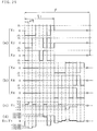
- Fig. 25 shows another example of the prior art in which a plurality of row electrodes are simultaneously selected and driven.
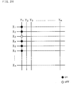
- a group of three lines each of the row electrodes are simultaneously selected at one time and the groups are selected in sequence in order to generate a display pattern, as shown in Fig. 26.
- row electrodes X1, X2 and X3 are selected and row voltages such as those shown in Fig. 25 (a) are applied to these row electrodes, X1, X2 and X3.
- the designated column voltages are applied to each column electrode Y1 to Y m .
- row electrodes X4, X5 and X6, shown in Fig. 26, are selected and row voltage such as that in Fig. 25 (b) is applied to these electrodes in the same manner as described above.
- column voltage is applied to each column electrode, Y1 to Y m .
- One frame will be the selection of all of the row electrodes, X1 to X n , in Fig. 26, and this cycle will be repeated continuously.
- each row voltage waveform described above is based on h as the number of row electrodes that are simultaneously selected, as in prior art Example 2, the number of 2 h row-select pattern are used. In this example, the number of 23 patterns are used.
- the voltage across a pixel should be as high as possible for an ON pixel and as low as possible for an OFF pixel.
- driving took place by dividing the selection period either into two or four intervals and separating them two times or four times within one frame F.
- the number of times of the division can be any number desired.
- the voltage waveforms which are applied to the row electrodes and the column electrodes and composed of eight pulse patterns or blocks as shown in the prior art Example in Fig. 25, are divided and separated in 8 intervals having equal period respectively and delivered one for each pulse pattern.
- the initial pulse within the eight pulse patterns will be applied to the selected row electrodes in Fig. 25.
- column voltage waveforms of the designated voltage level will be applied to each column electrode Y1 to Y m .
- the selection pulse is applied eight times within one frame, the unselected period of each pixel between two successive selected periods, that is, the OFF period, will be even shorter.
- the ON condition will be brighter and the OFF condition will be darker, allowing an increase in the contrast and reducing the amount of flicker.
- the shortest pulse width of Fig. 15 (c) and Fig. 16 above is 2 ⁇ t, which allows a pulse width to enlarge double.
- V column V(i) (0 ⁇ i ⁇ h) In either case, V column has h + 1 levels.
- Original voltage level Original number of mismatches
- the voltage levels that are applied to the column electrodes can be reduced by assuming the polarity and the display data of the selection pulse to be applied to the virtual row electrodes in this manner, and by making the number of mismatches always an odd number of one and three. In the embodiment above, they can be reduced to two levels. However, as stated above, they also may be made into even numbers. By reversing each polarity of the applied voltage in the F1 period and the applied voltage in F2 period, alternating current drive scheme is realized.
Landscapes
- Engineering & Computer Science (AREA)
- Chemical & Material Sciences (AREA)
- Crystallography & Structural Chemistry (AREA)
- Physics & Mathematics (AREA)
- Computer Hardware Design (AREA)
- General Physics & Mathematics (AREA)
- Theoretical Computer Science (AREA)
- Liquid Crystal Display Device Control (AREA)
- Liquid Crystal (AREA)
- Control Of Indicators Other Than Cathode Ray Tubes (AREA)
Abstract
Description
- The present invention concerns a driving method, and drive circuit for liquid crystal cells such as, for example, a liquid crystal display panel. The invention further concerns a liquid crystal display device.
- In the prior art, multiplex driving based on the amplitude selective addressing scheme is known as one method of driving the liquid crystal cells mentioned above.
- Fig. 21 shows a drawing of applied voltage waveforms that illustrate one example of the prior art driving method of multiplex driving a simple matrix type liquid crystal cell such as that shown in Fig. 22, which operates according to the amplitude selective addressing scheme. Figs. 21 (a) and 21 (b) show the voltage waveforms that will be applied to row electrodes X₁ and X₂, respectively. Fig. 21 (c) shows the waveform to be applied to column electrode Y₁. Fig. 21 (d) shows the voltage waveform that will be applied to the pixel defined by the column electrode Y₁ and the row electrode X₁.
- In this example driving is performed by applying the row voltage to one line each of row electrodes X₁, X₂ .... Xn selected in sequence and by applying at the same time the column voltage to column electrodes Y₁, Y₂ .... Ym depending on whether each pixel on the selected row electrode is ON or OFF.
- However, in order to select and drive the one line of the row electrodes mentioned above, it requires a relatively high voltage to achieve a good display.
- For this reason, in order to decrease the drive voltage mentioned above, a method in which more than one address line (row electrode) is selected simultaneously in sequence has been proposed. ("A Generalized Addressing Technique for RMS Responding Matrix LCDs," 1988 International Display Research Conference, pp. 80-85).
- As indicated above, Fig. 23 shows a drawing of one example of the conventional simultaneous selection and driving of a group comprising a plurality of row electrodes and sequential selection of the groups. In Fig. 23, (a) indicates the voltage waveforms applied to row electrodes X₁ and X₂. (b) indicates the voltage waveforms applied to row electrodes X₃ and X₄. (c) indicates the voltage waveform applied to column electrode Y₁. (d) indicates the voltage waveform applied to the pixel defined by the column electrode Y₁ and the row electrode X₁.
- This example is such that the display pattern shown in Fig. 22 mentioned above is displayed by sequentially selecting groups of two simultaneously selected row electrodes each. At first, two row electrodes, X₁ and X₂, are selected and a row voltage such as that shown in Fig. 23 (a) is, for example, applied to each. At the same time, the designated column voltage, which is described below, is applied to each column electrode, Y₁ to Ym. Next, row electrodes X₃ and X₄ are selected and the same type of row voltage as that described above is applied to these. At the same time, column voltage is applied to each column electrode, Y₁ to Ym. One frame represents the selection of all row electrodes, X₁ to Xn, and this cycle is repeated continuously.
- The voltage waveforms applied to the row electrodes described above use 2h row-select patterns when the number of row electrodes that are selected simultaneously is h. In this example, the number of 2² = 4 row-select patterns are used.
- The column voltage applied to each column electrode Y₁ to Ym provides the same number of pulse patterns as that of the row select pulse patterns, and are determined by comparing the state of ON or OFF of pixels on simultaneously selected row electrodes with the state of positive or negative of the voltage pulses applied to these row electrodes.
- In this example, as shown in the previously described Fig. 23, when row electrodes X₁ and X₂ are selected and row voltages such as those in Fig. 23 (a) and Fig. 24 (a) are applied to them, and when the pixels on row electrodes X₁ and X₂, are ON and OFF in sequence, the Ya column voltage waveform in Fig. 24 (b) is applied. When they are OFF and ON in sequence, the Yb column voltage waveform is applied. When they are both ON, the Yc column voltage waveform is applied. When they are both OFF, the Yd column voltage waveform is applied.
- The above-mentioned column voltage waveform is determined as follows. At first, it is defined that 1 represents the positive polarity of the voltage applied to a row electrode of the simultaneously selected row electrodes and -1 represents the negative polarity. Next, it is defined that -1 represents the ON display state of a pixel on each row electrode and 1 represents the OFF display state. Further, when the row-select pattern and the display data pattern are compared bit-by-bit, the difference between the number of matches and the number of mismatches is calculated. When the difference is two, V₂ is applied; when 0, V₀ is applied; and when -2, - V₂ is applied.
- For example, in the case of the above-mentioned column voltage waveform of Ya the display data pattern is [-1, 1] because the pixels on row electrodes X₁ and X₂ are ON and OFF, respectively. In contrast to this, pulse waveforms at the row electrodes, X₁ and X₂, in the first half of time interval t₁ in Fig. 24 are both negative providing a row-select pattern of [-1, -1]. When these are compared in sequence, the first combination matches, being -1 and -1, but the next combination does not, being -1 and 1. Thus, the number of matches is 1 and the number of mismatches is also 1. Therefore, the difference between the number of matches and the number of mismatches is zero. Thus, zero volts will be applied to the first half of time interval t₁ of Ya.
- Next, concerning the pulse waveforms of the second half of the above described time interval t₁, applied voltage of row electrode X₁ is positive and applied voltage of row electrode pulse X₂ is negative resulting in a row-select pattern of [1, -1]. When this is compared in sequence with the [-1, 1] display data pattern of the pixels described above are , the number of matches is zero and the number of mismatches is 2. Thus, -V₂ volts will be applied to the second half of time interval t₁.
- The pulse waveforms of the first half of time interval t₂ in Fig. 24 are represented by [-1, 1] because the voltage applied to row electrode X₁ is negative and the voltage applied to row electrode X₂ is positive. When these are compared with the display data pattern [-1, 1] of the pixels in sequence, the number of matches is two and the number of mismatches is zero. The difference between the number of matches and the number of mismatches is 2. Thus, V₂ volts will be applied to Ya in the first half of time interval t₂.
- Moreover, in the case of the pulse waveforms of the second half of time interval t₂, the voltages applied to row electrodes X₁ and X₂ are both positive. Thus, the pattern is [1, 1]. When compared to the pixels' display data pattern of [-1, 1], the number of matches is 1 and the number of mismatches is 1, making the difference between the number of matches and the number of mismatches zero. Thus, zero volts will be applied to Ya for the second half of time interval t₂.
- As for the other column voltage waveforms, Yb to Yd, the voltage will be set under the same type of guidelines as described above.
- In this regard, with the driving method of Fig. 23, when driving is according to the display pattern in Fig. 22, the display pattern on row electrodes X₁ and X₂, which corresponds to column electrode Y₁ of Fig. 22, will be ON and OFF in sequence. Thus, a column voltage equivalent to the aforesaid Ya will be applied to column electrode Y₁, as shown in Fig. 23 (c).
- In the examples above, the positive polarity of row-select voltage is represented by 1 and the negative by -1, and when the display state of each pixel is ON, it is represented by - 1, when OFF, by 1. The column voltage waveforms were selected based on the difference between the number of matches and the number of mismatches. However, either may be 1 or -1. Moreover, it also is possible to set the column voltage waveforms based on only the number of matches or the number of mismatches, without having to calculate the difference between the number of matches and the number of mismatches.
- Fig. 25 shows another example of the prior art in which a plurality of row electrodes are simultaneously selected and driven. In this example, a group of three lines each of the row electrodes are simultaneously selected at one time and the groups are selected in sequence in order to generate a display pattern, as shown in Fig. 26.
- In other words, initially three row electrodes, X₁, X₂ and X₃, are selected and row voltages such as those shown in Fig. 25 (a) are applied to these row electrodes, X₁, X₂ and X₃. At the same time, the designated column voltages, to be discussed later, are applied to each column electrode Y₁ to Ym. Next, row electrodes X₄, X₅ and X₆, shown in Fig. 26, are selected and row voltage such as that in Fig. 25 (b) is applied to these electrodes in the same manner as described above. At the same time, column voltage is applied to each column electrode, Y₁ to Ym. One frame will be the selection of all of the row electrodes, X₁ to Xn, in Fig. 26, and this cycle will be repeated continuously.
- When each row voltage waveform described above is based on h as the number of row electrodes that are simultaneously selected, as in prior art Example 2, the number of 2h row-select pattern are used. In this example, the number of 2³ patterns are used.
- Moreover, as in the previous example, the number of patterns of column voltages applied to each column electrode, Y₁ to Ym, is the same as the number of row-select patterns. The column voltage level is determined by comparing the row-select pattern and display pattern. Thus, for example, when the row voltage waveforms applied to row electrodes X₁, X₂ and X₃, which are selected simultaneously in this example, have a positive pulse, they are defined to be ON, and when they have a negative pulse, they are defined to be OFF. The ON and the OFF of the display data are compared at each pulse and the column voltage waveforms are set according to the number of mismatches.
- In other words, in Fig. 25, when the number of mismatches is zero, -V₃ volts are applied. When it is 1, -V₂ volts are applied. When it is 2, V₂ volts are applied. When it is 3, V₃ volts are applied. The voltage ratios for V₂ and V₃ above are set such that V₂ : V₃ = 1 : 3
- In specific terms, in the case of the voltage waveforms applied to row electrodes X₁, X₂ and X₃ in Fig. 25, they are ON when V₁ volts are applied and OFF when -V₁ volts are applied. Assuming the display of a pixel in Fig. 26 is ON when there is a black circle and OFF when there is an open circle, the display of the pixels at the intersections of column electrode Y₁ and row electrodes X₁, X₂ and X₃ in Fig. 26 will be ON, ON and OFF in sequence. In contrast to this, the initial pulse pattern of the voltage applied to each row electrode, X₁, X₂ and X₃, is OFF, OFF and OFF, respectively. Comparing both in sequence, the number of mismatches is 2. Therefore, V₂ volts are applied as the initial pulse to the electrode Y₁, as shown in Fig. 25 (c).
- In addition, the second pulse pattern of the voltage that is applied to each row electrode, X₁, X₂ and X₃, is OFF, OFF and ON, respectively. When comparing in sequence the voltage pattern with the ON, ON and OFF sequence of the aforesaid pixel display pattern, all are mismatching. Since the number of mismatches is 3, voltage V₃ is applied as the second pulse to column electrode Y₁. Under like guidelines, V₂ is applied as the third pulse and -V₂ is applied as the fourth pulse. The following voltages will be in the sequence -V₃, V₂, -V₂ and -V₂.
- The next three row electrodes, X₄ to X₆, will then be selected. When the voltage shown in Fig. 25 (b) is applied to row electrodes X₄ to X₆, a column voltage pattern of voltage levels that correspond to the mismatch between the ON and OFF displays of the pixels located where each of row electrodes X₄ to X₆ and a respective column electrode cross, and the ON and OFF of each pulse pattern of the voltage applied to each of the above described row electrodes X₄ to X₆ will be as the one shown in Fig. 25 (c) for column electrode Y₁. In Fig. 25, (d) are the voltage waveforms that are applied to the pixel at the crossing point of row electrode X₁ and column electrode Y₁. That is, it is the synthesized waveform between the voltage waveform applied to row electrode X₁ and the voltage waveform applied to column electrode Y₁.
- As indicated above, the method that simultaneously selects a plurality of row electrodes in a group and selects each group in sequence has the advantage of reducing drive voltage.
- Next, the general requirements, guidelines and procedures, etc., of the method that simultaneously selects a plurality of row electrodes of one of plural groups at one time and selects the groups in sequence and drives them will be described in sequence.
-
- (a) The number N of row electrodes is to be divided up into N/h subgroups.
- (b) Each subgroup will have h address lines.
- (c) At a time for addressing, the display data pattern on each column electrode is represented by an h-bit word.
dk*h+1, dk*h+2 .... dk*h+h; dk*h+j = 0 or 1
where 0 ≦ k ≦ (N/h) - 1 (k: subgroup)
In other words, one column of display data is:
d₁, d₂ .... dh ....Subgroup 0
dh+1, dh+2 .... dh+h ....Subgroup 1
dN-h+1, dN-h+2 .... dN-h+h .... Subgroup N/h-1 - (d) The row-select pattern has a 2h cycle and is represented by an h-bit word.
ak*h+1, ak*h+2 .... ak*h+h; ak*h+j = 0 or 1 -
- (1) The row electrodes of one subgroup are selected simultaneously for addressing.
- (2) One h-bit word is selected as the row-select pattern.
- (3) The row-select voltage is:
-Vr for alogic 0 in said h-bit row-select pattern word,
+Vr for alogic 1 in said h-bit row-select pattern word,
0 volts for the unselected period. - (4) The row-select patterns and the display data patterns in the selected subgroup are compared bit-by-bit.
- (5) The number of mismatches i between these two patterns is determined by

- (6) The column voltage is chosen to be V(i) when the number of mismatches is i.
- (7) The column voltages for each column in the matrix is determined independently by repeating the steps (4)-(6).
- (8) Both the row voltage and column voltage are applied simultaneously to the matrix display for a time duration Δt, where Δt is minimum pulse width.
- (9) A new row-select pattern is chosen and the column voltages are determined using steps (4)-(6). The new row and column voltages are applied to the display for an equal duration of time at the end of Δt.
- (10) A cycle is completed when all the subgroups (= N/h) have been selected once with all the 2h row-select patterns.

- The row select patterns in a case in which there are i number of mismatches will be considered. The number of h-bit row-select patterns which differ from an h-bit display data pattern by i bits is given by

For example, when the case for h=3 and row electrode selection pattern = (0,0,0) are considered, the results would be as shown in the table below:Mismatching number Display Data pattern Ci i = 0 (0,0,0) 1 way i = 1 (0,0,1) (0,1,0) (1,0,0) 3 ways i = 2 (1,1,0) (1,0,1) (0,1,1) 3 ways i = 3 (1,1,1) 1 way - These are determined by the number of bits of a word, not the row electrode selection patterns.
- If the amplitude Vpixel of the instantaneous voltage that is applied to the pixel had a row voltage of Vrow and column voltage of Vcolumn, the following would occur:

where, if


If


That is:

As a consequence, the specific amplitude to be applied to the pixel will be -(Vr + V(i)) or (Vr - V(i)) in the selection row and will be V(i) in the non-selection row. (When considering V(i) to be bipolar, the description becomes as in the previously described literature.) - In general, in order to achieve a high selection ratio, it is desirable that the voltage across a pixel should be as high as possible for an ON pixel and as low as possible for an OFF pixel.
- As a result, when ON:
The voltage |Vr + V(i)| is favorable for the ON pixel and The voltage |Vr - V(i)| is unfavorable for the ON pixel. - When OFF:
The voltage |Vr - V(i)| is favorable for the OFF pixel and The voltage |Vr + V(i)| functions unfavorable for the OFF pixel. - Here, it is favorable for the ON pixel to increase the effective voltage and unfavorable for the ON pixel to decrease the effective voltage. The number of combinations that selects i units from among the h bits is:

The number of mismatches gives the number of unfavorable voltages in the selected rows in a column. The total number of mismatches is i·Ci in Ci because every Ci row select patterns have i mismatches. Hence the number of unfavorable voltages per pixel (Bi) when number of mismatches is i can be obtained as given following;

The number of times a pixel gets a favorable voltage during the Ci time intervals considered is:

In addition:

Accordingly, the following is obtained:

Where: h ≧ i + 1
To summarize the above:



In addition:


and

However, as shown in Fig. 27, with the driving methods of the prior art, as shown in prior art Examples 1 to 3 above, in the first frame, for example, after the selection voltage has been applied to a certain pixel, during the period until the next selection voltage is applied to that pixel, the brightness will gradually decrease along with the elapse of time t. This will reduce the transmission rate T in the ON condition and, on the other hand, slightly increase the transmission rate T in the OFF condition. This will create deficiencies, such as poor contrast between the ON condition and the OFF condition. - Moreover, as shown in Fig. 25, in prior art Example 3 above, the pulse width applied to the row electrodes and the column electrodes narrows as the number of simultaneously selected row electrodes increases, and this increases the amount of crosstalk due to the distortion of the waveforms and causes problems, such as poor image quality. This problem becomes even more serious, for example, in a case in which gray shade display, which is caused by the pulse width modulation (PWM), takes place.
- Because this invention was proposed in consideration of the problem points of the prior art as described above, its objectives are to allow excellent driving for liquid crystal cells with a lot of electrodes in particular and to offer a driving method, a drive circuit and a liquid crystal display device for liquid crystal cells with excellent display performance.
- For this reason, the liquid crystal cell multiplex driving method according to the present invention wherein the liquid crystal cell comprises a liquid crystal layer located in between a substrate having row electrodes and a substrate having column electrodes, simultaneously selects a plurality of row electrodes continuously, and further this selection period is divided into multiple times within one frame.
- By adopting a driving method like that described above, for example, after selection voltage has been applied to a certain pixel in the initial frame, the voltage will be applied to that pixel several times during the period until selection voltage is applied to that pixel in the next frame. This makes it possible to maintain brightness and prevent a reduction in contrast.
- In addition, for the drive circuit of the liquid crystal cells of this invention, the row-select pattern data generated from the row electrode data generation circuit and the display data pattern on a plurality of row electrodes in correspondence to a column electrode, which are read in sequence from the frame memory and are selected simultaneously, will be calculated by an arithmetic operation circuit. The converted data, which will be the result of the calculation, will be transferred to the column electrode driver. The row-select pattern generated by the row electrode data generation circuit will be transferred to the row electrode driver. When one screen of row-select pattern has finished scanning, the above operation will be repeated by the next row-select pattern and display data pattern. The configuration is such that the operation will repeat a plurality of times in one frame period.
- By having a drive circuit such as that described above, it becomes possible to execute the driving method described above easily and reliably.
- Additionally, the display device of this invention has a driving circuit which performs the steps of calculating the row-select pattern generated by the row electrode data generation circuit and the display data pattern on the plurality of row electrodes which are read in sequence from the frame memory and is selected simultaneously with the row-select pattern. The driving circuit transfers the converted data, which is the result of the calculation, to the column electrode driver, transferring the row data, which is generated by the row electrode data generation circuit, to the row electrode driver. Further, the driving circuit repeats the above-mentioned operation by the next row-select pattern data and display data pattern when scanning of one screen is finished; and the screen operation is repeated several times in one frame period.
- By being configured as described above, it is possible to offer a display device with excellent contrast.
-
- Fig. 1
- shows a drawing of the applied voltage waveforms that represent the first embodiment of the driving method of the liquid crystal cells of this invention.
- Fig. 2
- shows a top view of the general configuration of the liquid crystal display.
- Fig. 3
- shows a graph that shows the relationship between the applied voltage that goes to the pixels and the transmission rate in the embodiments.
- Fig. 4
- shows a block diagram of the first embodiment of the drive circuit.
- Fig. 5
- shows a block diagram of the row electrode driver.
- Fig. 6
- shows a block diagram of the column electrode driver.
- Fig. 7
- shows a drawing of the applied voltage waveforms of another embodiment of the driving method of the liquid crystal cells of this invention.
- Fig. 8
- shows a drawing of the applied voltage waveforms of another embodiment of the driving method of the liquid crystal elements of this invention.
- Fig. 9
- is a drawing that describes the display patterns.
- Fig. 10
- shows a drawing of the applied voltage waveforms that go to the column electrodes that correspond to the display patterns.
- Fig. 11
- shows the applied voltage waveforms of another embodiment of the driving method of the liquid crystal elements of this invention.
- Fig. 12
- is a drawing that describes the display patterns.
- Fig. 13 (a)
- shows a drawing of the applied voltage waveforms that is applied to the row electrodes.
- Fig. 13 (b)
- shows a drawing of the applied voltage waveforms that go to the column electrodes that correspond to the display patterns.
- Fig. 14
- shows a drawing of the applied voltage waveforms that show another embodiment of the driving method of the liquid crystal cells of this invention.
- Fig. 15
- is a drawing that describes another example of the applied voltage waveforms that is applied to the row electrodes.
- Fig. 16
- shows the applied voltage waveforms in a case in which another row voltage is applied and driving takes place.
- Fig. 17
- shows a drawing of the applied voltage waveforms that show another embodiment of the driving method of the liquid crystal elements of this invention.
- Fig. 18
- is a drawing that shows a layout example of the virtual electrodes.
- Fig. 19
- shows a drawing of the applied voltage waveforms that show another embodiment of the driving method of the liquid crystal cells of this invention.
- Fig. 20
- is a drawing that describes the guidelines that reduce the column voltage level by using the virtual electrodes.
- Fig. 21
- shows the applied voltage waveforms that show one example of the driving method of the liquid crystal cell of the prior art.
- Fig. 22
- is a drawing that describes the display patterns.
- Fig. 23
- shows the applied voltage waveforms that show another example of the driving method of the liquid crystal elements of the prior art.
- Fig. 24
- is a drawing that describes the column voltage waveforms that are applied to the column electrodes in accordance with the display patterns.
- Fig. 25
- shows a drawing of the applied voltage waveforms that show another example of the driving method of the liquid crystal elements of the prior art.
- Fig. 26
- is a drawing that describes the display patterns.
- Fig. 27
- shows a graph that shows the relationship between the applied voltage that goes to the pixels and the transmission rate of the prior art.
- Below, a specific description of the driving method of the liquid crystal cells, the drive circuit and the display device of this invention will be given based on the embodiments indicated in the drawings.
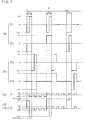
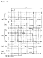
- Fig. 1 shows a drawing of the applied voltage waveforms that represent the first embodiment of the driving method of the liquid crystal cells of this invention. (a) in this drawing represents the voltage waveforms applied to row electrodes X₁ and X₂. (b) in this drawing represents the voltage waveforms applied to row electrodes X₃ and X₄. (c) in this drawing represents the voltage waveforms applied to column electrode Y₁. (d) in this drawing represents the voltage waveforms applied to the pixel at the crossing point of row electrode X₁ and column electrode Y₁.
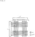
- Fig. 2 shows a top view of the general configuration of the liquid crystal display of the liquid crystal cells (liquid crystal display module) that are driven by applying the voltage described above. In this drawing, 1 is the row electrode driver; 2 is the column electrode driver; X₁, X₂ .... Xn are row electrodes; and Y₁, Y₂ .... Ym are column electrodes.
- This embodiment implements the type of display shown in Fig. 2 by dividing the selection period in two intervals and separating them within one frame F and driving, as in the case of the method shown in aforesaid Fig. 23 in the aforesaid Example of the prior art. That is, as shown in Fig. 1, first row electrodes X₁ and X₂ are selected. Then, for the time duration t₁ the same row voltage as in Fig. 23 is applied to row electrodes X₁ and X₂. At the same time, the column voltage set under the same guidelines as in the aforesaid prior art Example is applied to each column electrode, Y₁ to Ym. Next, row electrodes X₃ and X₄ are selected and the same row voltage as that for the above row electrodes X₁ and X₂ is applied to them. At the same time column voltage is applied in the same manner to each column electrode, Y₁ to Ym. This process is repeated until all of the row electrodes have been selected.
- Next, row electrodes X₁ and X₂ are selected once again and for the time duration t₂ the row voltage, which is shown in Fig. 23, is applied to them. At the same time column voltage is applied to each column electrode, Y₁ to Ym. This is repeated until all of the row electrodes, X₁ to Xn, have been selected. By carrying out the above operations within one frame F, one screen of display takes place. This is repeated in sequence.
- By driving as indicated above, the optical response shown in Fig. 3 is obtained. What is clear from a comparison with the prior art Example shown in Fig. 27 is that because brighter bright state is possible in the ON condition than in the prior art and because darker dark state is possible in the OFF condition than in the prior art, it is possible to improve the contrast and to reduce flicker.
- Next, examples of the configuration of the drive circuit that implements the driving method like that above will be described based on Fig. 4 through Fig. 6.
- Fig. 4 is a block diagram showing one example of the drive circuit. In this drawing, 1 represents the row electrode driver; 2 represents the column electrode driver; 3 represents the frame memory; 4 represents the arithmetic operations circuit; 5 represents the row electrode data generation circuit; and 6 represents a latch.
- Fig. 5 shows a block diagram of the row electrode driver. In this drawing, 11 is a shift register; 12 is a latch; 13 is a decoder; and 14 is a level shifter.
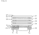
- Fig. 6 shows a block diagram of the column electrode driver. In this drawing, 21 a shift register; 22 is a latch; 23 is a decoder; and 24 is a level shifter.
- With the configuration indicated above, each voltage waveform that is applied to row electrodes will be generated by positive selection data or negative selection data or unselected data. This data is generated by row electrode
data generation circuit 5 shown in Fig. 4. This data will be transferred to rowelectrode driver 1. - As shown in Fig. 5, in
row electrode driver 1, row-select pattern signal S3 from row electrodedata generation circuit 5 will be transferred to shiftregister 11 by row shift clock signal S5. After the data of each row electrode in one scanning period have been transferred, each data will be latched by latch signal S6. The data that indicates the condition of each row electrode will be decoded bydecoder 13, and, vialevel shifter 14, turn on one of the three switches ofanalog switch 15 at each output. When the positive polarity has been selected, V₁ volts will be applied to the selected row electrode. When the negative polarity has been selected, -V₁ volts will be applied to the selected row electrode. During the unselected period, zero volts will be applied to the selected row electrode. - One the other hand, display data signal S1, which corresponds to each two row electrodes selected simultaneously, will be read from
memory 3 for generating each column voltage waveform. Then the row-select data from row-select pattern signal S3 will be latched. Display data signal S1 and row-select pattern data signal S4 will be converted byarithmetic operations circuit 4. Data conversion step will be performed, for example, under the guidelines described in the aforesaid technology of the prior art, and the data will then be transferred tocolumn electrode driver 2. - As shown in Fig. 6, with
column electrode driver 2, data signal S2 fromarithmetic operations circuit 4 will be transferred to shiftregister 21 by shift clock signal S7. After each column electrode data during one scanning period has been transferred, each data will be latched inlatch 22 by latch signal S8 and the data that indicates the condition of each column electrode will be decoded. One out of the three switches in each stage ofanalog switch 25 will be turned on and either V₂ volts, -V₂ volts or zero volts will be applied to each column electrode. - By using a drive circuit such as that described above, it is possible to easily and reliably implement the aforesaid type of driving method. In addition, if the above described drive circuit is provided for a display device that has the aforesaid type of display elements, and the aforesaid type of driving method is such that it can be executed, a display device with high contrast can be obtained.
- In the above embodiment, the selection period was divided in two intervals in one frame F and voltage was applied. However, it is possible to divide it up into two or more times, for example, four times. In addition, in the embodiment described above, the row electrodes were selected two at a time according to the array sequence. However, it also is possible to make the selection without necessarily following the array sequence. Such modifications will also be possible in the embodiments to be described below.
- Fig. 7 shows a drawing of applied voltage waveforms that show another embodiment of the driving method of the liquid crystal display cells of this invention. For each frame F, this embodiment alternately exchanges the row voltage waveforms applied to the row electrodes that are selected simultaneously. Other configurations are the same as the first embodiment.
- As described above, if for each frame F, the alternately exchanged row voltage waveforms are applied to the row electrodes that are selected simultaneously, it is possible to prevent pictures on the display from generating non-uniformity caused by differences in the applied voltage waveforms.
- In addition, because in this embodiment the selection period is divided in two intervals which are separated within one frame F, and voltage is applied, just as with the aforesaid first embodiment, the contrast will improve and flickering also can be reduced.
- Further, in this embodiment, it is also possible to use a drive circuit that is the same as the drive circuit that is explained in the aforesaid embodiment, and to provide a display device having a high display quality as well. In the aforesaid embodiment, the row voltage waveforms were exchanged after each frame. However, they also can be exchanged after each plurality of frames.
- The description of the aforesaid first embodiment and second embodiment provided an example in which two row electrodes were selected simultaneously. However, as in the embodiments to be described below, it also is possible to drive by selecting three or more row electrodes simultaneously. In such a case, as in the second embodiment, it is possible to cyclically exchange among each other every frame or every plurality of frames the row voltage waveforms that are applied to the row electrodes that are selected simultaneously.
- Fig. 8 shows a drawing of the applied voltage waveforms of another embodiment of the driving method of the liquid crystal cells of this invention. (a) in this drawing represents the voltage waveforms applied to row electrodes X₁ and X₂. (b) in this drawing represents the voltage waveforms applied to row electrodes X₃ and X₄. (c) in this drawing represents the voltage waveforms applied to column electrode Y₁. (d) in this drawing represents the voltage waveforms applied to the pixel at the crossing point of row electrode X₁ and column electrode Y₁.
- As in the aforesaid first embodiment, in this embodiment, two row electrodes are selected simultaneously. The row voltage with the voltage waveform shown in Fig. 8 (a) is applied to the row electrodes that are selected simultaneously. A display such as that shown in Fig. 2 takes place by dividing the selection period in two within one frame and driving.
- The sequence of the row electrode selection is the same as that in the aforesaid first embodiment. First, row electrodes X₁ and X₂ are selected and row voltage is applied to these electrodes for a time duration t₁. At the same time, the designated column voltage, which corresponds to the display data, is applied to all of the column electrodes Y₁ to Ym. Next, row electrodes X₃ and X₄ are selected and the same row voltage as with the aforesaid row electrodes X₁ and X₂ is applied to them for the time duration t₁₁. At the same time, the designated column voltage, which corresponds to the display data pattern, is applied to all of the column electrodes Y₁ to Ym. This is repeated until all of the row electrodes X₁ to Xn have been selected.
- Next, row electrodes X₁ and X₂ are selected once again and row voltage is applied to them for the time duration t₂. At the same time, the designated column voltage, which corresponds to the display data, is applied to all of the column electrodes Y₁ to Ym. Next, row electrodes X₃ and X₄ are selected and the same row voltage as the aforesaid row electrodes, X₁ and X₂, is applied to them for the time duration t₁₂. At the same time, the designated column voltage, which corresponds to the display data, is applied to all of the column electrodes Y₁ to Ym. This is repeated until all of the row electrodes X₁ to Xn have been selected. By executing the foregoing operation within one frame F, one display screen takes place, and this is repeated in sequence.
- In this embodiment, the polarity of the row voltage of waveforms applied to each row electrode is reversed every frame, which is what is called alternating current drive scheme. In such a case, it is possible to reverse the polarities every multiple of frames. In addition, it also is possible to apply the alternating current driving method mentioned above to the previously described embodiments and to the embodiments to be described below.
- Since the column voltage that is set under the same guidelines as in the aforesaid prior art Example 2 and the first embodiment is such that it is applied to the previously described column electrodes Y₁ to Ym, those guidelines will be described based on Fig. 9 and Fig. 10.
- Fig. 9 shows four types of display patterns of the pixels on, for example, row electrodes X₁ and X₂, which are selected simultaneously. That is, in the drawing, with the solid circles representing ON and the open circles representing OFF, display pattern on line a indicates that the pixels on both row electrodes X₁ and X₂ are both OFF. Display pattern on line b indicates that the pixel on row electrode X₁ is OFF and that the pixel on row electrode X₂ is ON. Display pattern on line c indicates that the pixel on row electrode X₁ is ON and that the pixel on row electrode X₂ is OFF. Display pattern on line d indicates that the pixels both row electrodes X₁ and X₂ are ON.
- Fig. 10 shows the relationship between the row voltage waveforms applied to the row electrodes that are selected simultaneously and the signal waveforms applied to each column electrode. X₁ and X₂ of Fig. 10 (a) represent the scanning waveforms applied to row electrodes X₁ and X₂. Ya to Yd of Fig. 10 (b) represent the column voltage waveforms applied to column electrodes Y₁ to Ym in correspondence to display patterns on lines a to d of Fig. 9.
- In other words, when the pixels on both row electrodes X₁ and X₂ are both OFF, as in display pattern a in Fig. 9, the Ya column voltage waveforms in Fig. 10 (b) will be applied. In the same manner, column voltage waveforms Yb, Yc and Yd will be applied to display patterns b, c and d, respectively.
- As in previously described prior art Example 2 and the first embodiment, in the case of the column voltage waveforms described above, it is assumed that when the row voltage pulse applied to row electrodes X₁ and X₂ is positive, this represented by a 1, if it is negative, by a -1. If a pixel is ON, this is represented by -1,if it is OFF, by 1. A comparison is performed at each pulse. When the difference between the number of matches and the number of mismatches is 2, V₂ volts will be applied. When it is zero, zero volts will be applied. When it is -2, -V₂ volts will be applied.
- For example, as in display pattern a in Fig. 9, when either of the pixels on row electrodes X₁ and X₂ is OFF, both will be represented by 1. When lined up in sequence, this becomes [1, 1]. In contrast to this, since the pulse waveform of row electrode X₁ is positive for a time duration t1 shown in Fig. 10, it is represented by 1. Since the pulse waveform of row electrode X₂ is negative, it is represented by -1. When lined up in sequence this becomes [1, -1]. When this [1, -1] and the [1, 1] of the above display pattern are compared in sequence, the former matches because there is a 1 and a 1. However, the latter does not match because there is a -1 and a 1.
- Since the number of matches is a 1 and the number of mismatches also is a 1, subtracting the number of mismatches from the number of matches yields zero. Thus, in the time duration t1 of Ya, zero volts will be applied. In addition, in the time duration t₂, since the pulse waveforms of row electrodes X₁ and X₂ are both positive, that yields a [1, 1]. When compared in sequence to the [1, 1] of the above described display pattern, both match. Thus, because the number of matches is two and the number of mismatches is zero, subtracting the number of mismatches from the number of matches yields a 2. Therefore, in the time duration t₂ of Ya, column voltage of V₂ volts will be applied.
- As for the other column voltage waveforms, Yb to Yd, the designated voltage will be applied according to the difference between the number of matches and the number of mismatches under the same guidelines.
- In this connection, in the driving method of Fig. 8 of this embodiment, which drives in response to the display pattern of previously described Fig. 2, the display patterns on row electrodes X₁ and X₂, which correspond to column electrode Y₁ of Fig. 2, will be ON and OFF. Therefore, this is equivalent to the display pattern on the line c of Fig. 9, and, as shown in Fig. 8 (c), column voltage that is equivalent to Yc will be applied to column electrode Y₁ for the time durations t₁ and t₂.
- In addition, the display pattern on row electrodes X₃ and X₄, which correspond to column electrode Y₁ of Fig. 2, also are ON and OFF and are equivalent to the display pattern on line c of Fig. 9. As shown in Fig. 8 (c), column voltage equivalent to Yc is applied to column electrode Y₁ for the time durations t₁₁ and t₁₂.
- As described above, pairs of two simultaneously selected row electrodes are selected in sequence in this embodiment as well. The same effect as in the previously described first embodiment will be obtained because they are driven by dividing the selection time period into two times in one frame F.
- Indeed, when 240 row electrodes were fabricated and the driving took place at drive voltages set to V₁ = 16.8 volts and V₂ = 2.1 volts, the same optical response as in the previously described Fig. 3 was obtained. In the ON condition, there was more brightness than in the prior art. In the OFF condition, there was more darkness than in the prior art. This allowed an improvement in the contrast and a reduction in flicker.
- Moreover, in the driving method of this embodiment, it also was possible to use a drive circuit that was almost the same as that of the first embodiment, which is shown in the previously described Fig. 4, a row electrode driver that was almost the same as that of the first embodiment, which is shown in Fig. 5, and a column electrode driver that was almost the same as that of the first embodiment, which is shown in Fig. 6. In such a case, as in the previously described embodiment, the calculation of the difference between the number of matches and number of mismatches takes place through
arithmetic operation circuit 4, which is shown in the previously mentioned Fig. 4. - A converted data signal will be transferred to the column electrode driver by
arithmetic operation circuit 4, and it need only generate the column voltage waveforms that will be applied to each column electrode. - By using a drive circuit such as that described above, it is possible to execute the previously described driving method simply and reliably. In addition, it also is possible to offer a display device that has excellent display performance.
- Fig. 11 shows a drawing of applied voltage waveforms that represent another embodiment of the driving method of the liquid crystal elements of this invention. Fig. 11 (a) shows the voltage waveforms that are applied to row electrodes X₁ to X₄. Fig. 11 (b) shows the voltage waveforms that are applied to row electrodes X₅ and X₆. Fig. 11 (c) shows the voltage waveform that is applied to column electrode Y₁. Fig. 11 (d) shows the voltage waveform that is applied to the pixel at the crossing point of row electrode X₁ and column electrode Y₁.
- This embodiment simultaneously selects four row electrodes each and applies voltage waveforms, such as that shown in Fig. 11 (a), to the simultaneously selected electrodes. In addition, by driving with the method of dividing the selection period into four intervals and distributing them in one frame, a display such as that shown in the previously described Fig. 2 will be provided.
- In other words, first, row electrodes X₁ to X₄ are selected and row voltage is applied to these row electrodes, X₁ to X₄, for the time duration t₁. At the same time, a designated column voltage that corresponds to the display data is applied to column electrodes Y₁ to Ym. Next, row electrodes X₅ to X₈ are selected. Due to paper space limitations, Fig. 11 (b) only shows row electrodes X₅ and X₆. The same row voltages as that for the previously described row electrodes X₁ to X₄ are applied to the selected row electrodes, X₅ to X₈, for the time duration t₁₁. At the same time, the designated column voltage that corresponds to the display data is applied to each column electrode, Y₁ to Ym. This is repeated until all of the row electrodes, X₁ to Xn, have been selected.
- Next, row electrodes X₁ to X₄ are selected once again and row voltage is applied to them during the time duration t₂. At the same time, the designated column voltage that corresponds to the display data will be applied to each column electrode, Y₁ to Ym. After this, row electrodes X₅ to X₈ are selected and the same row voltages as with the previously described row electrodes X₁ and X₂ are applied to them during the time duration t₁₂. At the same time, the designated column voltage that corresponds to the display data is applied to each column electrode, Y₁ to Ym. This is repeated until all of the row electrodes, X₁ to Xn, have been selected. By repeating the same operation as the above operation four times in one frame F, one screen of display will be performed.
- In this embodiment as well, by reversing the polarities of the row voltage waveforms that are applied to each row electrode in each one frame, the so-called alternating current drive scheme is employed.
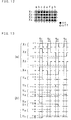
- Moreover, in this embodiment, column voltages that are set under almost the same guidelines as in the previously described third embodiment are applied to the above described column electrodes, Y₁ to Ym. The guidelines will be described based on Fig. 12 and Fig. 13.
- Fig. 12 shows a drawing of the display pattern that occurs on simultaneously selected row electrodes a column electrode, for example, row electrodes X₁ to X₄. In the drawing, with the black circles representing ON and the open circles representing OFF, eight examples of display patterns, from a to h, are given.
- Fig. 13 (a) shows the row voltage waveforms applied to each of the row electrodes, X₁ to X₄. Fig. 13 (b) shows the column voltage waveforms that are applied to column electrodes Y₁ to Ym in response to display patterns a to h in Fig. 12.
- That is to say, when the pixels on simultaneously selected row electrodes X₁ to X₄ are all OFF, as is, for example, display pattern on line a of Fig. 12, the Ya column voltage waveform in Fig. 13 (b) is applied. At the same time, column voltage waveform Yb is applied in the case of display pattern on line b. Column voltage waveform Yc is applied in the case of display pattern on line c. Column voltage waveform Yd is applied in the case of display pattern on line d. Column voltage waveform Ye is applied in the case of display pattern on line e. Column voltage waveform Yf is applied in the case of display pattern f. Column voltage waveform Yg is applied in the case of display pattern g. Column voltage waveform Yh is applied in the case of display pattern h.
- As in the previously described third embodiment, in the case of the column voltage waveforms described above, it is assumed that if the row voltage waveform applied to a row electrode X₁ to X₄ is a positive selection pulse, this is represented by a 1,a negative selection pulse by a -1. If a pixel display is ON, this is assumed to be represented by a -1, and if it is OFF, by a 1. The resulting patterns are compared bit-by-bit as in the previous embodiments and the number of matches and number of mismatches are calculated. When the difference between the number of matches and the number of mismatches is 4, V₃ volts will be applied. When the difference is 2, V₂ volts will be applied. When the difference is zero, zero volts will be applied. When the difference is -2, -V₂ volts will be applied. When the difference is -4, -V₃ volts will be applied. The ratio of the above described V₂ and V₃ volts is set to V₂: V₃ = 1:2.
- For example, as in the display pattern shown in Fig. 12, when all of the pixels on row electrodes X₁ to X₄ are OFF, each display will be represented by 1. When lined up in sequence, they yield a pattern of [1, 1, 1, 1]. The waveforms of row electrodes X₁ to X₄ in the time duration t1 shown in Fig. 13 (a) are all positive. So, they are all represented by 1. When lined up in sequence, they yield a pattern of [1, 1, 1, 1]. When both patterns are compared bit-by-bit, they all match. The number of matches amounts to four and the number of mismatches amounts to zero. Subtracting the mismatches from the matches yields a 4. Voltage of V₃ volts will be applied for the time duration t1 of Ya.
- In the time duration t₂, the waveforms of the four row electrodes X₁ to X₄ are positive, positive, negative and negative in sequence. Thus, in sequence, that is represented by the pattern [1, 1, -1, -1]. When compared in sequence to the [1, 1, 1, 1] of the display pattern described above, there are two matches and two mismatches. Subtracting the number of mismatches from the number of matches yields a zero. Thus, zero volts will be applied for the time duration t₂ of Ya. In the same manner, the waveforms of the four row electrodes X₁ to X₄ are positive and negative and positive and negative in sequence for the time duration t₃. Thus, in sequence, they are represented by [1, -1, 1, -1] Comparing this to the [1, 1, 1, 1] of the display pattern described above, there are two matches and two mismatches. Subtracting the number of mismatches from the number of matches yields a zero. Zero volts will be applied for the time duration t₃.
- Finally, since the waveforms of the four row electrodes X₁ to X₄ are positive, negative, negative and positive in sequence, this yields a pattern of [1, -1, -1, 1]. When compared to the [1, 1, 1, 1] of the above display pattern , there are two matches and two mismatches. Subtracting the number of mismatches from the number of matches yields zero. Zero volts of voltage will be applied for the time duration t₄ of Ya.
- Next, the display pattern shown in Fig. 12 (b) shows that the pixels on row electrodes X₁ to X₄ are ON, OFF, ON and OFF, which gives a display pattern of [-1, 1, -1, 1]. The waveforms of the row voltage for the time duration t1 of Fig. 13 (a) are all positive. Thus, in sequence, there are represented by [1, 1, 1, 1]. When each is compared in sequence, there are two matches and two mismatches. Subtracting the number of mismatches from the number of matches yields zero. Thus, zero volts will be applied during the time duration t1 of Yb.
- The waveforms of the four row electrodes X₁ to X₄ for the duration t₂ are positive, positive, negative and negative. In sequence, that corresponds to a pattern [1, 1, -1, -1]. When compared in sequence to the display pattern described above, which is [-1, 1, -1, 1], there are two matches and two mismatches. Subtracting the number of mismatches from the number of matches yields a zero. Thus, zero volts will be applied for the time duration t2 of Yb.
- In the same manner, the waveforms of the four row electrodes X₁ to X₄ for the time duration t₃ are positive, negative, positive and negative in sequence. That is, in sequence, they are represented by [1, -1, 1, -1]. When compared in sequence to the display pattern described above, all are mismatches, which yields zero matches and four mismatches. Subtracting the number of mismatches from the number of matches, yields a -4. Thus, -V₃ volts of voltage will be applied for the time duration t₃ of Yb.
- Finally, the waveforms of the four row electrodes X₁ to X₄ for the time duration t₄ in sequence are positive, negative, negative and positive, which yields in sequence [1, -1, -1, 1]. Compared in sequence to the [-1, 1, -1, 1] of the display pattern described above, there are two matches and two mismatches. Subtracting the number of mismatches from the number of matches yields a zero. Thus, zero volts will be applied for the time duration t₄ of Yb.
- Under the same guidelines for the other display patterns, c to h, when the difference between the number of matches and number of mismatches is 4, V₃ volts will be applied. When the difference is 2, V₂ volts will be applied. When the difference is 0, zero volts will be applied. When the difference is -2, -V₂ volts will be applied be applied. When the difference is -4, -V₃ volts will be applied. Column voltages Yc to Yh, which correspond to each display pattern, on line c to h, will be formed. In addition to the eight display patterns, on line a to h, shown in Fig. 12, it is possible to create additional eight display patterns. However, the column voltage waveforms will be formed under the same guidelines as above in the case of these eight display patterns as well.
- In this manner, the display pattern on the simultaneously selected row electrodes in correspondence to a column electrode and the row-select pattern applied to the selected electrodes are compared. By calculating the difference between the number of matches and the number of mismatches of data of patterns, column voltage that corresponds to the display content will be applied to each column electrode.
- In this connection, in the driving method of the previously described Fig. 11 of this embodiment, which drives according to the display pattern of previously described Fig. 2, the display pattern on the row electrodes, X₁ to X₄, that correspond to the column electrode Y₁ of Fig. 2 are ON, OFF, ON and OFF in sequence. Therefore, they are equivalent to display pattern b in Fig. 12. As shown in Fig. 11 (c), for the time durations t₁, t₂, t₃ and t₄, column voltage that is correspondence to Yb is applied to column electrode Y₁.
- As described above, in this embodiment as well, four row electrodes are selected in sequence and driving will be carried out by dividing the selection period into four intervals and separating them within the one frame F. Thus, the same effects gained in the previously described first embodiment can be obtained.
- Indeed, when fabricating 240 row electrodes and driving with the drive voltage as V₁ = 12 volts, V₂ = 1.5 volts, and V₃ = 3 volts, the optical response is the same as that shown in previously described Fig. 3. In the ON condition, they are brighter that those of the prior art. In the OFF condition, they are darker than those of the prior art. This allows an improvement in contrast and a reduction in flicker.
- In addition, in the driving method of this embodiment as well, a drive circuit that is almost the same as that of the previously described first embodiment, which is shown in Fig. 4, the row electrode driver shown in Fig. 5, and a column electrode driver that is almost the same as that in Fig. 6 can be used.
- In this case, as with the embodiments described above, the calculation of the difference between the number of matches and number of mismatches described above is carried out by
arithmetic operation circuit 4, which is shown in Fig. 4. A signal that has been data converted byarithmetic operation circuit 4 is transferred tocolumn electrode driver 2 and the column voltage waveforms that are applied to the column electrodes need only be generated. - At that time,
analog switch 25 of the column electrode driver shown in previously described Fig. 6 has a configuration that comprises three switches for each column electrode, Y₁ to Ym, inputs three types of voltages, V₂, 0 and -V₂, and outputs one of them. However, in this embodiment, it need only be a configuration that comprises five switches for each column electrode, Y₁ to Ym, and inputs five types of voltages, V₃, V₂, 0, -V₂ and -V₃, and outputs one of those voltages. - By using a drive circuit such as that described above, a driving method such as that described above can be executed simply and reliably and allows a display device that has excellent display performance to be provided.
- In the third embodiment and the fourth embodiment, driving took place by dividing the selection period either into two or four intervals and separating them two times or four times within one frame F. However, the number of times of the division can be any number desired.
- In addition, a description was given of the simultaneous selection of either two or four row electrodes in the third embodiment and the fourth embodiment described above. However, it is possible to drive by selecting three row electrodes or four or more row electrodes.
- Fig. 14 shows a drawing of the applied voltage waveforms that indicate the fifth embodiment of the driving method of the liquid crystal cells of this invention. In the Example of the prior art shown in previously described Fig. 25, a plurality of row electrodes are simultaneously selected and groups of simultaneously selected row electrodes are selected in sequence. In contrast to the selection period being one in one place within one frame F, in this invention, the selection period is divided and separated in several intervals within one frame F.
- In the case of the drawings in particular, the voltage waveforms, which are applied to the row electrodes and the column electrodes and composed of eight pulse patterns or blocks as shown in the prior art Example in Fig. 25, are divided and separated in 8 intervals having equal period respectively and delivered one for each pulse pattern.
- In this connection, as shown in Fig. 14, the initial pulses among the eight pulse patterns that were applied to each row electrode, X₁, X₂ and X₃, in Fig. 25 will be applied to the three row electrodes, X₁, X₂ and X₃, that were initially selected. At the same time, the column voltage waveforms of the designated voltage level, which corresponds to the number of mismatches between the selection pulse and display data under the same guideline as with the prior art Examples, will be applied to each column electrode Y₁ to Ym.
- Next, the initial pulse within the eight pulse patterns will be applied to the selected row electrodes in Fig. 25. At the same time, column voltage waveforms of the designated voltage level will be applied to each column electrode Y₁ to Ym.
- After scanning all of the row electrodes once, the second pulse among the previously mentioned eight pulses will be applied once again to the initial row electrodes, X₁,X₂ and X₃. Once previously mentioned eight pulse patterns have been applied to all of the row electrodes, one frame F will be finished.
- As indicated above, in this embodiment especially, since the selection pulse is applied eight times within one frame, the unselected period of each pixel between two successive selected periods, that is, the OFF period, will be even shorter. As in Fig. 3 above, the ON condition will be brighter and the OFF condition will be darker, allowing an increase in the contrast and reducing the amount of flicker.
- In addition, in the driving method of this embodiment, it is possible to use a drive circuit that is almost the same as that of the first embodiment, a row electrode driver that is almost the same as that of the first embodiment, and a column electrode driver that is almost the same as that of the first embodiment. In this case, as in the previously described embodiment, the calculation of the difference between the number of matches and number of mismatches takes place through
arithmetic operation circuit 4, which is shown in the previously described Fig. 4. The signal that underwent data conversion is transferred to a column electrode driver that is configured in the same manner as that in the previously described fourth embodiment, and the column voltage waveform to be applied to each column electrode is created. - In addition, by using a drive circuit such as that described above, it is possible to execute the previously described driving method simply and positively. In addition, it also is possible to offer a display device that has excellent display performance.
- The sequence for generating the selection pulse of each selection period in this embodiment is as desired. It also is possible to make appropriate changes within one frame F. Also, eight pulse patterns are divided into eight intervals in this embodiment. It is also possible to divide into four intervals and output two pulse patterns at a time four times in sequence.
- As stated above, the number of bit-word patterns when selecting and driving a plurality (h number) of row electrodes in sequence is 2h. For example, as in the aforesaid example, when h = 3, 2³ = 8 patterns. With ON represented by 1 and OFF by 0, the voltage ON and OFF pattern that applies these to row electrodes, X₁, X₂ and X₃, can be expressed as shown in the Table below.
X₁ 0 0 0 0 1 1 1 1 X₂ 0 0 1 1 0 0 1 1 X₃ 0 1 0 1 0 1 0 1 - If the voltage waveforms are applied to each row electrode based on this, they will be as shown in Fig. 15 (a). However, the waveforms in Fig. 15 (a) have many different frequency components, therefore, if actually used, there is the danger that display distortion will appear.
- For this reason, the arrangement is changed to eliminate the deviation of the frequency component. These are the waveforms in Fig. 15 (b). The prior art Example in Fig. 25 uses these waveforms.
- However, using the type of waveform in Fig. 15(b), not only those shown in Fig. 15 (a) above, when the number of row electrodes that are simultaneously selected increases, the number of above described bit-word patterns will increase exponentially. Along with this, each pulse width will have to become narrower. When actually applied to the pixel, there is a danger of rounding or distortion of a waveform. Further, when implementing gray shade display, for example, which are caused by the modulation of the pulse widths, the narrower pulse width becomes the cause of generating crosstalk.
- For this reason, in this embodiment, the voltage waveforms applied to the row electrodes are set under the following guidelines so that the pulse widths become wider.
- For applied voltage waveforms to the row electrodes, these are determined taking the following into consideration:
- (1) Each row electrode must be distinguishable.
- (2) The frequency components applied to each row electrode must not differ significantly.
- (3) The alternating current characteristics within one frame or within a plurality of frames must be guaranteed.
- In other words, the applied voltage patterns are to be appropriately selected, taking the conditions mentioned above into consideration, from among the systems of orthogonal functions, such as natural binary, Walsh and Hadamard.
- Among these, item number (1) is a necessary-sufficient condition. In particular, in order to satisfy item number (1), it has been decided that the applied voltage waveforms of each row electrode will each have different frequency components. What is decided by taking into considering the above conditions are the applied voltage waveforms in Fig. 15 (c). The applied voltage waveforms, which include different frequency components, are:



Fig. 16 shows drawings of applied voltage waveforms in a case in which the applied voltage waveforms to the row electrodes are formed based on the waveforms of Fig. 15 (c) above and the voltage waveforms to the column electrodes that relate to this are formed and driven under the same guidelines as in the prior art. - In contrast to the shortest pulse width in Figs. 15 (a) and (b) above and in contrast to the prior art Example in Fig. 25 above, which is Δt, the shortest pulse width of Fig. 15 (c) and Fig. 16 above is 2 Δt, which allows a pulse width to enlarge double. By making the pulse width large in this manner, it is possible to reduce the impact of the waveform rounding, thereby making it possible to reduce cross talk as well as making it possible to increase the number of simultaneously selected row electrodes.
- The waveforms of the embodiment described above are one example. They can be changed as appropriate. In addition, things such as the row electrode selection sequence and the arrangement sequence of the pulse patterns that are applied to each row electrode can be changed as desired.
- Fig. 17 shows examples in which the drive waveforms in Fig. 16 above are divided into a plurality of times within one frame F and applied, as in the fifth embodiment above.
- If carried out as indicated above, it is possible to increase the contrast of the ON and OFF conditions and reduce the amount of flicker, just as in the fifth embodiment. Further, it is possible to reduce crosstalk, which is caused by waveform distortion. It also is possible to use the same circuitry as that of the fifth embodiment as well as obtain the same kind of display device.
- In the embodiment described above, four levels, V₃, V₂, -V₂ and -V₃, were used as the column electrode voltage levels.
- However, the number of levels can be reduced under the following guidelines. First of all, a description will be given based on the general methods of reducing the number of previously mentioned voltage levels.
- In the aforementioned subgroup of h row electrodes, there are e virtual row electrodes (virtual lines). By controlling the matching and mismatching of this virtual row electrode data, the total number of matches and number of mismatches will be limited, and the number of drive voltage levels for column electrodes will be reduced.
- With Mi representing the number of mismatches and Vc representing an appropriate constant, Vcolumn, the applied voltage to the column electrode, will be as follows:

or, more simply:

In either case, Vcolumn has h + 1 levels. - For example, the case in which subgroup h = 4 and virtual row electrode e = 1 will be considered. As in the previous embodiment, the number of levels when h = 3 will be four levels, -V₃, -V₂, V₂ and V₃. If control takes place through the virtual row electrodes so that there is an even number of mismatches, the results will be as shown in the Table below.
Original voltage level Original number of mismatches Virtual row electrode Number of mismatches on revision Voltage levels on revision - V₃ 0 Match 0 Va - V₂ 1 Mismatch 2 Vb V₂ 2 Match 2 Vb V₃ 3 Mismatch 4 Vd - As shown above, it is possible to reduce original four levels to three levels. In addition, if the number of mismatches is made an odd number, the number of mismatches on revision in the above table will change in sequence from the top to 1, 1, 3 and 3. This will make it possible to have, for example, two levels in voltage.
- In addition, the voltage levels in a case in which the subgroup comprises h = 4 row electrodes and there are no reductions in voltage levels, will be five levels, for example, - V₃, -V₂, 0, V₂ and V₃. However, in contrast to requiring these five levels, if control takes place through the virtual row electrodes so that there is an even number of mismatches, the results would be as shown in the Table below.
Original voltage level Original number of mismatches Virtual row electrode Number of mismatches on revision Voltage levels on revision - V₃ 0 Match 0 Va - V₂ 1 Mismatch 2 V b0 2 Match 2 Vb V₂ 3 Mismatch 4 Vd V₃ 4 Match 4 Vd - As shown above, it is possible to reduce original five levels to three levels. In the above case, it is possible to set the voltage levels so that the number of mismatches is an odd number. As for the virtual row electrodes above, since normally they need not display, they do not necessarily have to be fabricated. However, it they are fabricated, they can be fabricated in an area where they will not effect the display. For example, as shown in Fig. 18, the virtual row electrodes Xn+1 and so on are fabricated on the outside of display region R in a device such as a liquid crystal display device. Or, if there are extra row electrodes on the outside of display region R, it also is possible to use them as virtual row electrodes.
- In addition, if the number e of virtual row electrodes is increased, the number of levels can be reduced even further. In such a case, if as above, e = 1, all of the numbers of mismatches will be controlled so that they can be divided by 2. For example, in the case of e = 2, the numbers of mismatches can all be controlled so that they can be divided by 3. However, they can all be divided by 3 and have 1 remaining or 2 remaining.
- Finally, the maximum number of reductions possible under the above method is 1/(e+1). When e = 1, it is 1/2, except for zero volts.
- Fig. 19 shows an example in which groups each of three row electrodes and one virtual row electrode are used to reduce the applied voltage level to the column electrodes. In this example as well, the selection period is divided into a plurality of times in one frame.
- This embodiment divides the selection period into four times in one frame and counts the number of aforesaid mismatches for the four row electrodes (including the virtual row electrode) for each period. It then makes the number of mismatches so that they always are an odd number, making the number of mismatches a one or a three. In response to this, the number of voltage levels of the column voltage waveform will become two levels, V₂ and -V₂.
- More specifically, for example, when creating the type of display shown in Fig. 18, after the initially selected row electrodes, X₁, X₂ and X₃, as shown in Fig. 20, will come virtual row electrode Xn+1. (Actually, virtual row electrodes need not really be existent as stated above. When they are existent, it is desirable to have them on the outside of display region R, as shown in Fig. 18.) When considering the time duration t1, assuming ON to represent a positive voltage being applied to the above row electrodes and OFF a negative voltage, and assuming that V₁, V₁ and -V₁ volts pulses will be applied to each row electrode, X₁, X₂ and X₃, respectively, and assuming that V₁ will be applied to the virtual row electrode Xn+1, and assuming the data that will be displayed by the pixels at the crossing point between column electrode Y₁ and virtual row electrode Xn+1 at that time to be OFF, the number of mismatches would be one, and a -V₂ voltage pulse should be applied to the column electrode.
- Next, looking at the t₂ period, assuming that V₁ is applied to virtual row electrode Xn+1, the number of mismatches is three, and voltage pulse V₂ should be applied to the column electrode. In addition, assuming that V₁ is applied to virtual row electrode Xn+1 in the t₃ period, there are three number of mismatches, and voltage pulse V₂ should be applied to the column electrode. Finally, assuming voltage pulse -V₁ is applied to virtual row electrode Xn+1 in the period t₄, there is one mismatch, and voltage pulse -V₂ should be applied to the column electrode.
- The voltage levels that are applied to the column electrodes can be reduced by assuming the polarity and the display data of the selection pulse to be applied to the virtual row electrodes in this manner, and by making the number of mismatches always an odd number of one and three. In the embodiment above, they can be reduced to two levels. However, as stated above, they also may be made into even numbers. By reversing each polarity of the applied voltage in the F₁ period and the applied voltage in F₂ period, alternating current drive scheme is realized.
- By reducing the number of voltage levels that are applied to the column electrodes as described above, the circuit configuration of things such as the liquid crystal drive can be simplified, allowing a drive circuit that is almost identical to that described in the previous embodiment(s) to be used. In addition, as in the previously described embodiment(s), this allows a display device with excellent display performance to be obtained.
- As described above, because the driving method, drive circuit and display device of the liquid crystal elements of this invention have the configurations described above, the effects that can be obtained are as follows:
- (1) Because groups each comprising a plurality of simultaneously selected row electrodes are selected in sequence, and because driving takes place by dividing the selection period into a plurality of times within one frame, as shown in Fig. 3, it is possible to have pixels that are brighter when ON and darker when OFF, which allows an improvement in contrast.
- (2) Because, by dividing, the selection pulse is applied in a plurality of intervals within one frame, flicker is not conspicuous. In addition, flicker is reduced even though the frame frequency is reduced, which reduces flicker as well as crosstalk.
- (3) It is possible to reduce the drive voltage to generate a display.
- (4) Because it is possible to reduce the number of different frequency components as described above, it also is possible to lengthen the pulse width and, by doing that, reduce crosstalk, which is caused by the rounding of the waveform. This allows an improvement in the image quality.
- As described above, a variety of effects will take place due to this invention. For example, by applying it to a variety of display devices, such as the liquid crystal displays of products such as computers and dedicated word processing machines, it is possible to improve things such as display quality and reliability.
Claims (8)
- A drive method of devices such as liquid crystal cells having substrates with electrodes and liquid crystal layer disposed between the substrates and driven by multiplex driving method; comprising the steps of selecting simultaneously a plurality of row electrodes in sequence during a selection period and dividing and separating the selection period into a plurality of intervals within one frame period.
- The drive method of devices such as liquid crystal cells described in claim 1, wherein comprising; dividing and separating a voltage waveform applied to a electrode and the column electrode into a plurality of intervals in one frame period, and applying the voltage of the divided voltage waveform to the row electrode and to the column electrode.
- The drive method of devices such as liquid crystal cells described in claim 1, wherein comprising; applying the column voltage determined according to the state of positive or negative of the row voltage pulse that is applied to row electrodes that are selected simultaneously and the state of the ON or OFF of the pixels on the row electrodes that are selected simultaneously.
- The drive method of devices such as liquid crystal cells described in claim 1, wherein comprising; replacing row selection voltage waveforms applied to the simultaneously selected row electrodes periodically.
- The drive method of devices such as liquid crystal cells described in claim 1, wherein comprising; enlarging a pulse width of row selection voltage waveform by selecting a pattern of a row selection voltage waveform from among a plurality of system of orthogonal functions.
- The drive method of devices such as liquid crystal cells described in claim 1, wherein comprising; reducing the number of voltage levels applied to a column electrode by a fabricating virtual row electrode.
- A drive circuit for devices such as a display device comprising; a row electrode data generating circuit which generates a row selection pulse data; a frame memory which generates a display data on a plurality of row electrodes which are selected simultaneously in sequence; an arithmetic operation circuit which calculating the converted data based on the row selection pulse data and display data, a column electrode driver which is inputted a converted data from the arithmetic operation circuit , and a row electrode driver which is inputted the row selection pulse data from row electrode data generating circuit, wherein scanning one screen is performed a plurality of times according to a row selection pulse data and a display data within one frame period.
- A display device comprising; a drive circuit having; a row electrode data generating circuit which generates a row selection pulse data; a frame memory which generates a display data on a plurality of row electrodes which are selected simultaneously in sequence; an arithmetic operation circuit which calculating the converted data based on the row selection pulse data and display data, a column electrode driver which is inputted a converted data from the arithmetic operation circuit , and a row electrode driver which is inputted the row selection pulse data from row electrode data generating circuit, wherein the drive circuit scans one screen a plurality of times according to a row selection pulse data and a display data within one frame period.
Applications Claiming Priority (10)
| Application Number | Priority Date | Filing Date | Title |
|---|---|---|---|
| JP4874392 | 1992-03-05 | ||
| JP4874392 | 1992-03-05 | ||
| JP48743/92 | 1992-03-05 | ||
| JP8400792 | 1992-04-06 | ||
| JP8400792 | 1992-04-06 | ||
| JP84007/92 | 1992-04-06 | ||
| JP143482/92 | 1992-05-08 | ||
| JP14348292 | 1992-05-08 | ||
| JP14348292 | 1992-05-08 | ||
| PCT/JP1993/000279 WO1993018501A1 (en) | 1992-03-05 | 1993-03-04 | Method and circuit for driving liquid crystal elements, and display apparatus |
Publications (3)
| Publication Number | Publication Date |
|---|---|
| EP0585466A1 true EP0585466A1 (en) | 1994-03-09 |
| EP0585466A4 EP0585466A4 (en) | 1996-11-06 |
| EP0585466B1 EP0585466B1 (en) | 1999-09-08 |
Family
ID=27293392
Family Applications (1)
| Application Number | Title | Priority Date | Filing Date |
|---|---|---|---|
| EP93905616A Expired - Lifetime EP0585466B1 (en) | 1992-03-05 | 1993-03-04 | Method and circuit for driving liquid crystal elements, and display apparatus |
Country Status (6)
| Country | Link |
|---|---|
| US (6) | US6084563A (en) |
| EP (1) | EP0585466B1 (en) |
| JP (1) | JP3508114B2 (en) |
| DE (1) | DE69326300T2 (en) |
| TW (1) | TW280900B (en) |
| WO (1) | WO1993018501A1 (en) |
Cited By (8)
| Publication number | Priority date | Publication date | Assignee | Title |
|---|---|---|---|---|
| EP0604226A3 (en) * | 1992-12-24 | 1996-04-10 | Seiko Instr Inc | Liquid crystal display device. |
| GB2295479A (en) * | 1992-07-07 | 1996-05-29 | Seiko Epson Corp | Matrix displays |
| US5596344A (en) * | 1991-07-08 | 1997-01-21 | Asahi Glass Company Ltd. | Driving method of driving a liquid crystal display element |
| US5739803A (en) * | 1994-01-24 | 1998-04-14 | Arithmos, Inc. | Electronic system for driving liquid crystal displays |
| US5805130A (en) * | 1994-04-27 | 1998-09-08 | Sharp Kabushiki Kaisha | Liquid crystal display device and method for driving the same |
| US5870070A (en) * | 1995-10-05 | 1999-02-09 | Sharp Kabushiki Kaisha | Liquid crystal display device and method for driving display device |
| US5929832A (en) * | 1995-03-28 | 1999-07-27 | Sharp Kabushiki Kaisha | Memory interface circuit and access method |
| EP1079364A4 (en) * | 1999-03-15 | 2003-01-02 | Seiko Epson Corp | LIQUID CRYSTAL DISPLAY AND OPERATION METHOD THEREOF |
Families Citing this family (29)
| Publication number | Priority date | Publication date | Assignee | Title |
|---|---|---|---|---|
| JP3582082B2 (en) | 1992-07-07 | 2004-10-27 | セイコーエプソン株式会社 | Matrix display device, matrix display control device, and matrix display drive device |
| US5900856A (en) | 1992-03-05 | 1999-05-04 | Seiko Epson Corporation | Matrix display apparatus, matrix display control apparatus, and matrix display drive apparatus |
| JP3508114B2 (en) * | 1992-03-05 | 2004-03-22 | セイコーエプソン株式会社 | Liquid crystal device, driving method thereof, and driving circuit |
| JP3365007B2 (en) | 1993-11-09 | 2003-01-08 | セイコーエプソン株式会社 | Liquid crystal device driving method and display device |
| WO1995034020A1 (en) | 1994-06-03 | 1995-12-14 | Seiko Epson Corporation | Method of driving liquid crystal display device, liquid crystal display device, electronic machine, and drive circuit |
| CN100505008C (en) | 1994-11-17 | 2009-06-24 | 精工爱普生株式会社 | Display device and electronic equipment containing display device |
| DE19510083C2 (en) * | 1995-03-20 | 1997-04-24 | Ibm | Method and arrangement for speech recognition in languages containing word composites |
| JP3856919B2 (en) * | 1997-08-29 | 2006-12-13 | 株式会社東芝 | Liquid crystal display |
| TW428158B (en) * | 1998-02-24 | 2001-04-01 | Nippon Electric Co | Method and device for driving liquid crystal display element |
| JP3410952B2 (en) * | 1998-02-27 | 2003-05-26 | シャープ株式会社 | Liquid crystal display device and driving method thereof |
| JP3403635B2 (en) * | 1998-03-26 | 2003-05-06 | 富士通株式会社 | Display device and method of driving the display device |
| GB9807184D0 (en) * | 1998-04-04 | 1998-06-03 | Philips Electronics Nv | Active matrix liquid crystal display devices |
| US6919876B1 (en) * | 1999-02-26 | 2005-07-19 | Optrex Corporation | Driving method and driving device for a display device |
| US20030147017A1 (en) * | 2000-02-15 | 2003-08-07 | Jean-Daniel Bonny | Display device with multiple row addressing |
| US7362294B2 (en) * | 2000-04-26 | 2008-04-22 | Jps Group Holdings, Ltd | Low power LCD with gray shade driving scheme |
| US6970151B1 (en) * | 2000-09-01 | 2005-11-29 | Rockwell Collins | Display controller with spread-spectrum timing to minimize electromagnetic emissions |
| US6803897B2 (en) * | 2000-12-22 | 2004-10-12 | Koninklijke Philips Electronics N.V. | Display device with freely programmable multiplex rate |
| EP1396838A4 (en) * | 2001-06-13 | 2008-04-30 | Kawasaki Microelectronics Inc | Simple matrix liquid crystal drive method and apparatus |
| JP3632637B2 (en) | 2001-08-09 | 2005-03-23 | セイコーエプソン株式会社 | Electro-optical device, driving method thereof, driving circuit of electro-optical device, and electronic apparatus |
| KR100486295B1 (en) * | 2002-12-31 | 2005-04-29 | 삼성전자주식회사 | Multi-line selection driving method of super-twisted nematic Liquid Crystal Display having low-power consumption |
| JP2004348077A (en) * | 2003-05-26 | 2004-12-09 | Seiko Epson Corp | Driving circuit and its inspection method, electro-optical device, and electronic equipment |
| US20060184718A1 (en) * | 2005-02-16 | 2006-08-17 | Sinclair Alan W | Direct file data programming and deletion in flash memories |
| US20070001964A1 (en) * | 2005-06-30 | 2007-01-04 | Lg.Philips Lcd Co., Ltd. | Display device and method of driving the same |
| KR20110103722A (en) * | 2010-03-15 | 2011-09-21 | 삼성전자주식회사 | Electrophoretic display device and its driving method |
| US8866783B2 (en) | 2011-04-08 | 2014-10-21 | Sharp Kabushiki Kaisha | Display device, method for driving same, and electronic apparatus |
| US9165509B2 (en) | 2011-04-28 | 2015-10-20 | Sharp Kabushiki Kaisha | Display module, display device comprising same, and electronic device |
| TWI451393B (en) * | 2011-10-14 | 2014-09-01 | Sitronix Technology Corp | A driving method of a liquid crystal display device and a driving circuit thereof |
| KR102266064B1 (en) * | 2014-10-15 | 2021-06-18 | 삼성디스플레이 주식회사 | Method of driving display panel, display panel driving apparatus and display apparatus having the display panel driving apparatus |
| US12437729B2 (en) * | 2023-03-29 | 2025-10-07 | Panasonic Automotive Systems Co., Ltd. | Dimming device, display device, and method for driving dimming device |
Family Cites Families (35)
| Publication number | Priority date | Publication date | Assignee | Title |
|---|---|---|---|---|
| JPS5715393B2 (en) * | 1973-04-20 | 1982-03-30 | ||
| US4100579A (en) * | 1974-09-24 | 1978-07-11 | Hughes Aircraft Company | AC Operated flat panel liquid crystal display |
| JPS5156118A (en) | 1974-11-13 | 1976-05-17 | Japan Broadcasting Corp | PANERUDEI SUPURE ISOCHI |
| JPS5422856A (en) * | 1977-07-22 | 1979-02-21 | Kokusai Electric Co Ltd | Method of detecting position of moving body |
| US4266130A (en) | 1978-10-13 | 1981-05-05 | The United States Of America As Represented By The Secretary Of Commerce | Method and apparatus for detecting clear air turbulences |
| JPS5715393A (en) * | 1980-06-30 | 1982-01-26 | Matsushita Electric Industrial Co Ltd | Sheathed heater |
| CH645473A5 (en) * | 1980-08-05 | 1984-09-28 | Videlec Ag | Method for activating a liquid crystal display |
| DE3482365D1 (en) * | 1984-11-08 | 1990-06-28 | Itt Ind Gmbh Deutsche | TELEVISION RECEIVER WITH FLICKER-FREE PLAYBACK OF AN INTERMEDIATE VIDEO SIGNAL. |
| JPS61262724A (en) | 1985-05-08 | 1986-11-20 | Stanley Electric Co Ltd | Liquid crystal display device |
| JPS62102230A (en) | 1985-10-30 | 1987-05-12 | Seiko Epson Corp | Driving method for liquid crystal element |
| US5041821A (en) * | 1987-04-03 | 1991-08-20 | Canon Kabushiki Kaisha | Ferroelectric liquid crystal apparatus with temperature dependent DC offset voltage |
| US4873516A (en) * | 1987-06-01 | 1989-10-10 | General Electric Company | Method and system for eliminating cross-talk in thin film transistor matrix addressed liquid crystal displays |
| JP2675060B2 (en) * | 1988-04-20 | 1997-11-12 | 株式会社日立製作所 | Active matrix display device, scanning circuit thereof, and driving circuit of scanning circuit |
| FR2633764B1 (en) * | 1988-06-29 | 1991-02-15 | Commissariat Energie Atomique | METHOD AND DEVICE FOR CONTROLLING A MATRIX SCREEN DISPLAYING GRAY LEVELS |
| DE69027136T2 (en) * | 1989-02-10 | 1996-10-24 | Sharp Kk | Liquid crystal display unit and control method therefor |
| EP0388976A3 (en) * | 1989-03-28 | 1991-06-05 | In Focus Systems, Inc. | Color display |
| DE4031905C2 (en) * | 1989-10-09 | 1993-12-09 | Hitachi Ltd | Multi-level display system and method for displaying gray tones with such a system |
| JP2823614B2 (en) * | 1989-12-15 | 1998-11-11 | 株式会社日立製作所 | Gradation display method and liquid crystal display device |
| US5103144A (en) * | 1990-10-01 | 1992-04-07 | Raytheon Company | Brightness control for flat panel display |
| US5459495A (en) * | 1992-05-14 | 1995-10-17 | In Focus Systems, Inc. | Gray level addressing for LCDs |
| US5485173A (en) * | 1991-04-01 | 1996-01-16 | In Focus Systems, Inc. | LCD addressing system and method |
| US5280280A (en) * | 1991-05-24 | 1994-01-18 | Robert Hotto | DC integrating display driver employing pixel status memories |
| US5489919A (en) | 1991-07-08 | 1996-02-06 | Asashi Glass Company Ltd. | Driving method of driving a liquid crystal display element |
| JP3368926B2 (en) | 1992-04-22 | 2003-01-20 | 旭硝子株式会社 | Driving method of liquid crystal display element |
| JP3119737B2 (en) | 1991-08-16 | 2000-12-25 | 旭硝子株式会社 | Driving method and driving circuit for liquid crystal display element |
| JP3373226B2 (en) | 1991-07-08 | 2003-02-04 | 旭硝子株式会社 | Driving method of liquid crystal display element |
| DE69214206T2 (en) | 1991-07-08 | 1997-03-13 | Asahi Glass Co. Ltd., Tokio/Tokyo | Control method for a liquid crystal display element |
| JP3508114B2 (en) * | 1992-03-05 | 2004-03-22 | セイコーエプソン株式会社 | Liquid crystal device, driving method thereof, and driving circuit |
| NL194875C (en) * | 1992-04-01 | 2003-05-06 | Citizen Watch Co Ltd | Display device containing a liquid crystal material. |
| US5621425A (en) | 1992-12-24 | 1997-04-15 | Seiko Instruments Inc. | Liquid crystal display device |
| CA2164982A1 (en) * | 1993-06-30 | 1995-01-12 | Arlie R. Conner | Real time active addressing display device and method utilizing fast walsh transform circuit |
| US5475397A (en) * | 1993-07-12 | 1995-12-12 | Motorola, Inc. | Method and apparatus for reducing discontinuities in an active addressing display system |
| JP3185490B2 (en) | 1993-09-09 | 2001-07-09 | 富士電機株式会社 | High frequency induction heating device |
| US5626881A (en) | 1995-05-16 | 1997-05-06 | Menefee Mining Corporation | Humate dietary supplement |
| US5778523A (en) | 1996-11-08 | 1998-07-14 | W. L. Gore & Associates, Inc. | Method for controlling warp of electronic assemblies by use of package stiffener |
-
1993
- 1993-03-04 JP JP51553193A patent/JP3508114B2/en not_active Expired - Lifetime
- 1993-03-04 WO PCT/JP1993/000279 patent/WO1993018501A1/en not_active Ceased
- 1993-03-04 DE DE69326300T patent/DE69326300T2/en not_active Expired - Lifetime
- 1993-03-04 EP EP93905616A patent/EP0585466B1/en not_active Expired - Lifetime
- 1993-06-17 TW TW082104839A patent/TW280900B/zh not_active IP Right Cessation
- 1993-11-04 US US08/148,083 patent/US6084563A/en not_active Expired - Lifetime
-
1995
- 1995-05-31 US US08/457,688 patent/US5963189A/en not_active Expired - Lifetime
-
1999
- 1999-03-26 US US09/277,585 patent/US6208323B1/en not_active Expired - Fee Related
- 1999-03-29 US US09/281,997 patent/US6252573B1/en not_active Expired - Fee Related
-
2001
- 2001-03-28 US US09/821,063 patent/US6421040B2/en not_active Expired - Fee Related
-
2002
- 2002-06-07 US US10/164,984 patent/US7095397B2/en not_active Expired - Fee Related
Cited By (11)
| Publication number | Priority date | Publication date | Assignee | Title |
|---|---|---|---|---|
| US5596344A (en) * | 1991-07-08 | 1997-01-21 | Asahi Glass Company Ltd. | Driving method of driving a liquid crystal display element |
| GB2295479A (en) * | 1992-07-07 | 1996-05-29 | Seiko Epson Corp | Matrix displays |
| GB2295479B (en) * | 1992-07-07 | 1996-11-13 | Seiko Epson Corp | Matrix displays |
| EP0604226A3 (en) * | 1992-12-24 | 1996-04-10 | Seiko Instr Inc | Liquid crystal display device. |
| EP0807921A1 (en) * | 1992-12-24 | 1997-11-19 | Seiko Instruments Inc. | Liquid crystal display device |
| US5739803A (en) * | 1994-01-24 | 1998-04-14 | Arithmos, Inc. | Electronic system for driving liquid crystal displays |
| US5805130A (en) * | 1994-04-27 | 1998-09-08 | Sharp Kabushiki Kaisha | Liquid crystal display device and method for driving the same |
| US5929832A (en) * | 1995-03-28 | 1999-07-27 | Sharp Kabushiki Kaisha | Memory interface circuit and access method |
| US5870070A (en) * | 1995-10-05 | 1999-02-09 | Sharp Kabushiki Kaisha | Liquid crystal display device and method for driving display device |
| EP1079364A4 (en) * | 1999-03-15 | 2003-01-02 | Seiko Epson Corp | LIQUID CRYSTAL DISPLAY AND OPERATION METHOD THEREOF |
| US6657610B1 (en) | 1999-03-15 | 2003-12-02 | Seiko Epson Corporation | Liquid-crystal display device and method of driving the same |
Also Published As
| Publication number | Publication date |
|---|---|
| WO1993018501A1 (en) | 1993-09-16 |
| US5963189A (en) | 1999-10-05 |
| US7095397B2 (en) | 2006-08-22 |
| DE69326300T2 (en) | 2000-02-24 |
| DE69326300D1 (en) | 1999-10-14 |
| US20010030636A1 (en) | 2001-10-18 |
| US6252573B1 (en) | 2001-06-26 |
| EP0585466B1 (en) | 1999-09-08 |
| EP0585466A4 (en) | 1996-11-06 |
| US6084563A (en) | 2000-07-04 |
| JP3508114B2 (en) | 2004-03-22 |
| US20030043099A1 (en) | 2003-03-06 |
| US6208323B1 (en) | 2001-03-27 |
| US6421040B2 (en) | 2002-07-16 |
| TW280900B (en) | 1996-07-11 |
Similar Documents
| Publication | Publication Date | Title |
|---|---|---|
| EP0585466B1 (en) | Method and circuit for driving liquid crystal elements, and display apparatus | |
| US5877738A (en) | Liquid crystal element drive method, drive circuit, and display apparatus | |
| EP0366117B1 (en) | Liquid crystal apparatus | |
| JP3084293B2 (en) | LCD driver IC with pixel inversion operation | |
| JPWO1993018501A1 (en) | Driving method and driving circuit for liquid crystal element, etc., and display device | |
| US4702560A (en) | Liquid crystal display device | |
| US5508716A (en) | Plural line liquid crystal addressing method and apparatus | |
| EP0618562A1 (en) | A display apparatus and a driving method for a display apparatus | |
| EP0836173B1 (en) | Multiplex driving method of a matrix type liquid crystal electro-optical device | |
| EP0581255A1 (en) | A method of driving display element and its driving device | |
| EP0661683B1 (en) | Liquid crystal display panel driving device | |
| JPWO1993023844A1 (en) | Driving method and driving circuit for liquid crystal element, etc., and display device | |
| US5959603A (en) | Liquid crystal element drive method, drive circuit, and display apparatus | |
| US6972779B2 (en) | Flat-panel display device | |
| US6271820B1 (en) | Light modulating devices | |
| EP0617399B1 (en) | Liquid crystal display apparatus | |
| KR100438659B1 (en) | Column Driver Integrated Circuit And Column Driving Method For Pre_Driving Liquid Crystal Display | |
| JP3391048B2 (en) | Liquid crystal device driving method, liquid crystal device driving circuit, and display device | |
| JPH0772454A (en) | Liquid crystal display | |
| JP3501157B2 (en) | Method and circuit for driving liquid crystal device and liquid crystal device | |
| US5969703A (en) | Multiplex addressing using auxiliary pulses | |
| JP3570757B2 (en) | Driving method of image display device | |
| JP2001109440A (en) | Driving method and driving circuit for liquid crystal element and display device | |
| JP2000275606A (en) | Driving method of liquid crystal device, liquid crystal display device and driving circuit | |
| JP2001108963A (en) | Driving method of liquid crystal device, liquid crystal display device and driving circuit |
Legal Events
| Date | Code | Title | Description |
|---|---|---|---|
| PUAI | Public reference made under article 153(3) epc to a published international application that has entered the european phase |
Free format text: ORIGINAL CODE: 0009012 |
|
| 17P | Request for examination filed |
Effective date: 19931105 |
|
| AK | Designated contracting states |
Kind code of ref document: A1 Designated state(s): DE FR GB NL |
|
| A4 | Supplementary search report drawn up and despatched | ||
| AK | Designated contracting states |
Kind code of ref document: A4 Designated state(s): DE FR GB NL |
|
| 17Q | First examination report despatched |
Effective date: 19970605 |
|
| GRAG | Despatch of communication of intention to grant |
Free format text: ORIGINAL CODE: EPIDOS AGRA |
|
| GRAG | Despatch of communication of intention to grant |
Free format text: ORIGINAL CODE: EPIDOS AGRA |
|
| GRAH | Despatch of communication of intention to grant a patent |
Free format text: ORIGINAL CODE: EPIDOS IGRA |
|
| GRAG | Despatch of communication of intention to grant |
Free format text: ORIGINAL CODE: EPIDOS AGRA |
|
| GRAH | Despatch of communication of intention to grant a patent |
Free format text: ORIGINAL CODE: EPIDOS IGRA |
|
| GRAG | Despatch of communication of intention to grant |
Free format text: ORIGINAL CODE: EPIDOS AGRA |
|
| GRAG | Despatch of communication of intention to grant |
Free format text: ORIGINAL CODE: EPIDOS AGRA |
|
| GRAH | Despatch of communication of intention to grant a patent |
Free format text: ORIGINAL CODE: EPIDOS IGRA |
|
| GRAH | Despatch of communication of intention to grant a patent |
Free format text: ORIGINAL CODE: EPIDOS IGRA |
|
| GRAA | (expected) grant |
Free format text: ORIGINAL CODE: 0009210 |
|
| AK | Designated contracting states |
Kind code of ref document: B1 Designated state(s): DE FR GB NL |
|
| REF | Corresponds to: |
Ref document number: 69326300 Country of ref document: DE Date of ref document: 19991014 |
|
| ET | Fr: translation filed | ||
| PLBE | No opposition filed within time limit |
Free format text: ORIGINAL CODE: 0009261 |
|
| STAA | Information on the status of an ep patent application or granted ep patent |
Free format text: STATUS: NO OPPOSITION FILED WITHIN TIME LIMIT |
|
| 26N | No opposition filed | ||
| REG | Reference to a national code |
Ref country code: GB Ref legal event code: IF02 |
|
| PGFP | Annual fee paid to national office [announced via postgrant information from national office to epo] |
Ref country code: FR Payment date: 20120319 Year of fee payment: 20 |
|
| PGFP | Annual fee paid to national office [announced via postgrant information from national office to epo] |
Ref country code: GB Payment date: 20120301 Year of fee payment: 20 |
|
| PGFP | Annual fee paid to national office [announced via postgrant information from national office to epo] |
Ref country code: DE Payment date: 20120404 Year of fee payment: 20 Ref country code: NL Payment date: 20120322 Year of fee payment: 20 |
|
| REG | Reference to a national code |
Ref country code: DE Ref legal event code: R071 Ref document number: 69326300 Country of ref document: DE |
|
| REG | Reference to a national code |
Ref country code: NL Ref legal event code: V4 Effective date: 20130304 |
|
| REG | Reference to a national code |
Ref country code: GB Ref legal event code: PE20 Expiry date: 20130303 |
|
| PG25 | Lapsed in a contracting state [announced via postgrant information from national office to epo] |
Ref country code: GB Free format text: LAPSE BECAUSE OF EXPIRATION OF PROTECTION Effective date: 20130303 Ref country code: DE Free format text: LAPSE BECAUSE OF EXPIRATION OF PROTECTION Effective date: 20130305 |