EP0583097A1 - Module hermaphrodite pour noeud de signaux à terminal double - Google Patents
Module hermaphrodite pour noeud de signaux à terminal double Download PDFInfo
- Publication number
- EP0583097A1 EP0583097A1 EP93305826A EP93305826A EP0583097A1 EP 0583097 A1 EP0583097 A1 EP 0583097A1 EP 93305826 A EP93305826 A EP 93305826A EP 93305826 A EP93305826 A EP 93305826A EP 0583097 A1 EP0583097 A1 EP 0583097A1
- Authority
- EP
- European Patent Office
- Prior art keywords
- pressure table
- housing
- contacts
- flexible circuit
- recited
- Prior art date
- Legal status (The legal status is an assumption and is not a legal conclusion. Google has not performed a legal analysis and makes no representation as to the accuracy of the status listed.)
- Granted
Links
Images


Classifications
-
- H—ELECTRICITY
- H01—ELECTRIC ELEMENTS
- H01R—ELECTRICALLY-CONDUCTIVE CONNECTIONS; STRUCTURAL ASSOCIATIONS OF A PLURALITY OF MUTUALLY-INSULATED ELECTRICAL CONNECTING ELEMENTS; COUPLING DEVICES; CURRENT COLLECTORS
- H01R12/00—Structural associations of a plurality of mutually-insulated electrical connecting elements, specially adapted for printed circuits, e.g. printed circuit boards [PCB], flat or ribbon cables, or like generally planar structures, e.g. terminal strips, terminal blocks; Coupling devices specially adapted for printed circuits, flat or ribbon cables, or like generally planar structures; Terminals specially adapted for contact with, or insertion into, printed circuits, flat or ribbon cables, or like generally planar structures
- H01R12/70—Coupling devices
- H01R12/77—Coupling devices for flexible printed circuits, flat or ribbon cables or like structures
- H01R12/79—Coupling devices for flexible printed circuits, flat or ribbon cables or like structures connecting to rigid printed circuits or like structures
-
- G—PHYSICS
- G01—MEASURING; TESTING
- G01R—MEASURING ELECTRIC VARIABLES; MEASURING MAGNETIC VARIABLES
- G01R1/00—Details of instruments or arrangements of the types included in groups G01R5/00 - G01R13/00 and G01R31/00
- G01R1/02—General constructional details
- G01R1/04—Housings; Supporting members; Arrangements of terminals
- G01R1/0408—Test fixtures or contact fields; Connectors or connecting adaptors; Test clips; Test sockets
- G01R1/0416—Connectors, terminals
-
- H—ELECTRICITY
- H01—ELECTRIC ELEMENTS
- H01R—ELECTRICALLY-CONDUCTIVE CONNECTIONS; STRUCTURAL ASSOCIATIONS OF A PLURALITY OF MUTUALLY-INSULATED ELECTRICAL CONNECTING ELEMENTS; COUPLING DEVICES; CURRENT COLLECTORS
- H01R24/00—Two-part coupling devices, or either of their cooperating parts, characterised by their overall structure
- H01R24/84—Hermaphroditic coupling devices
-
- H—ELECTRICITY
- H01—ELECTRIC ELEMENTS
- H01R—ELECTRICALLY-CONDUCTIVE CONNECTIONS; STRUCTURAL ASSOCIATIONS OF A PLURALITY OF MUTUALLY-INSULATED ELECTRICAL CONNECTING ELEMENTS; COUPLING DEVICES; CURRENT COLLECTORS
- H01R12/00—Structural associations of a plurality of mutually-insulated electrical connecting elements, specially adapted for printed circuits, e.g. printed circuit boards [PCB], flat or ribbon cables, or like generally planar structures, e.g. terminal strips, terminal blocks; Coupling devices specially adapted for printed circuits, flat or ribbon cables, or like generally planar structures; Terminals specially adapted for contact with, or insertion into, printed circuits, flat or ribbon cables, or like generally planar structures
- H01R12/70—Coupling devices
- H01R12/77—Coupling devices for flexible printed circuits, flat or ribbon cables or like structures
- H01R12/771—Details
- H01R12/775—Ground or shield arrangements
-
- H—ELECTRICITY
- H01—ELECTRIC ELEMENTS
- H01R—ELECTRICALLY-CONDUCTIVE CONNECTIONS; STRUCTURAL ASSOCIATIONS OF A PLURALITY OF MUTUALLY-INSULATED ELECTRICAL CONNECTING ELEMENTS; COUPLING DEVICES; CURRENT COLLECTORS
- H01R13/00—Details of coupling devices of the kinds covered by groups H01R12/70 or H01R24/00 - H01R33/00
- H01R13/648—Protective earth or shield arrangements on coupling devices, e.g. anti-static shielding
- H01R13/658—High frequency shielding arrangements, e.g. against EMI [Electro-Magnetic Interference] or EMP [Electro-Magnetic Pulse]
- H01R13/6581—Shield structure
- H01R13/6582—Shield structure with resilient means for engaging mating connector
- H01R13/6583—Shield structure with resilient means for engaging mating connector with separate conductive resilient members between mating shield members
-
- H—ELECTRICITY
- H01—ELECTRIC ELEMENTS
- H01R—ELECTRICALLY-CONDUCTIVE CONNECTIONS; STRUCTURAL ASSOCIATIONS OF A PLURALITY OF MUTUALLY-INSULATED ELECTRICAL CONNECTING ELEMENTS; COUPLING DEVICES; CURRENT COLLECTORS
- H01R13/00—Details of coupling devices of the kinds covered by groups H01R12/70 or H01R24/00 - H01R33/00
- H01R13/648—Protective earth or shield arrangements on coupling devices, e.g. anti-static shielding
- H01R13/658—High frequency shielding arrangements, e.g. against EMI [Electro-Magnetic Interference] or EMP [Electro-Magnetic Pulse]
- H01R13/6581—Shield structure
- H01R13/6585—Shielding material individually surrounding or interposed between mutually spaced contacts
- H01R13/6588—Shielding material individually surrounding or interposed between mutually spaced contacts with through openings for individual contacts
-
- H—ELECTRICITY
- H01—ELECTRIC ELEMENTS
- H01R—ELECTRICALLY-CONDUCTIVE CONNECTIONS; STRUCTURAL ASSOCIATIONS OF A PLURALITY OF MUTUALLY-INSULATED ELECTRICAL CONNECTING ELEMENTS; COUPLING DEVICES; CURRENT COLLECTORS
- H01R13/00—Details of coupling devices of the kinds covered by groups H01R12/70 or H01R24/00 - H01R33/00
- H01R13/648—Protective earth or shield arrangements on coupling devices, e.g. anti-static shielding
- H01R13/658—High frequency shielding arrangements, e.g. against EMI [Electro-Magnetic Interference] or EMP [Electro-Magnetic Pulse]
- H01R13/6591—Specific features or arrangements of connection of shield to conductive members
- H01R13/6594—Specific features or arrangements of connection of shield to conductive members the shield being mounted on a PCB and connected to conductive members
- H01R13/6595—Specific features or arrangements of connection of shield to conductive members the shield being mounted on a PCB and connected to conductive members with separate members fixing the shield to the PCB
Definitions
- This invention relates to electrical connectors, and in particular to a connector for interconnecting printed circuit boards.
- the present invention provides an hermaphroditic node module which includes a flexible circuit having two arrays of exposed contacts in planes at 90 degrees to each other. Each of these portions of the flexible circuit is mounted on a pressure table which is biased outwardly of a connector body by means of one or more compression springs.
- the pressure table for the forward face of the connector that mates with an identical connector has freedom for limited floating movement to help assure proper interengagement of the mating sets of contacts.
- a resilient pad on the outer face of the pressure table distributes the mating force equally and compensates for minor variations in surface contour.
- the pressure table for the other array of contacts is confined to a rectilinear path of movement, inasmuch as it is to be connected to a flat printed circuit board. Again a resilient pad is employed beneath the contact array.
- the pressure table for the mating face of the connector includes forwardly projecting side flanges the edges of which are to engage the flange edges of an identical connector to assist in the alignment and positioning of the two connectors.
- a grounding clip may be included, extending around the forward pressure table and provided with forwardly projecting tabs which engage the grounding clip of the mating connector.
- the grounding clip connects to the grounding plane of the flexible circuit through the brass rivets that retain the flexible circuit to the pressure table. Grounding contacts on the flexible circuit provide additional shielding. In this manner, 360 degree shielding can be achieved.
- the conductors that interconnect the two sets of contacts of the flexible circuit are all of the same length. Therefore the circuit paths and the impedance are the same for all interconnected contacts.
- a ground plane layer is provided on the entire underside of the flexible circuit.
- the connector is compact, self-aligning, requires zero insertion force at the interfaces, and has no pin-and-socket contacts with attendant wear and contact forces, as well as associated hardware. Higher density and greater interfacial positional zone tolerance for interconnections are achieved. It can interconnect in single pairs or in multiple arrays.
- the connector is superior to the earlier hermaphroditic connector referred to above by assuring more uniform contact pressure, self-alignment at the mating face, and permitting a higher force biasing the mating connectors together. A much higher contact density is made possible. It is also easier to assemble, is made largely of lightweight durable plastic parts, and is readily mounted in a carrier for supporting the connector. Unlike the earlier connector, the present invention provides fully shielded circuits with matching impedance of 50 ohms. The earlier design also lacks the grounding clip of the present invention.
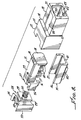
- the connector 10 for interconnecting printed circuit boards includes a hollow housing 11 of dielectric material which includes a forward section 12 and a rearward section 13. Both the forward and rearward sections are rectangular in cross section, but the forward section 12 is of larger lateral dimension than that of the rearward section 13. This provides an external shoulder 14 on both sides and at the top between the forward and rearward sections 12 and 13.
- a body 15 which has a forward portion 16 received in the forward part 12 of the housing 11 and a rearward portion 17 that is received within the rearward portion 13 of the housing 11.
- the rearward end of the body 15 terminates in a flat generally rectangular transverse disk 18 positioned at the open rearward end of the housing 11.
- a tab 19 projecting from the upper edge of the disk portion 18 is received in a notch 20 at the rearward end of the upper wall 21 of the rearward portion 13 of the housing 11. This prevents the member 15 from moving forwardly relative to the housing 11.
- a flat ridge 23 on the upper surface of the rearward portion 17 of the body 15 is complementarily received in an elongated slot 24 through the upper wall 21 of the housing 11.
- the rearward edge of the ridge 23 engages the rearward edge of the slot 24 which prevents the body 15 from moving rearwardly relative to the housing 11.
- a pressure table 28 of dielectric material is received in the open forward end 12 of the housing 11 and on either side includes a rearward flange 29 received between the arms 26 and 27 of the body 15.
- a compression spring 30 bears against the body 15 at one end and is received within a recess 31 in the rearward end of the pressure table 28 at its other end. This biases the pressure table 28 forwardly with respect to the housing 11 and the member 15, this movement being limited by the engagement of the flange 29 with the arms 26 and 27.
- the pressure table 28 has freedom for limited floating movement relative to the housing 11.
- Two parallel side flanges 33 and 34 extend from the forward end of the pressure table 28, projecting outwardly from the forward end of the housing 11.
- the rearward portion 13 of the housing 11 receives a second pressure table 35 which is generally U-shaped in cross section, as seen in FIGS. 5 and 8.
- the two side flanges 36 and 37 of the pressure table 35 fit around the opposite side edges 38 and 39 of the body 15 between the enlarged forward section 16 and the rearward disk 18. This holds the pressure table 35 against movement longitudinally of the body 15 and housing 11.
- the thickened central portion 40 of the lower wall 41 of the pressure table 35 protrudes through an opening 42 in the bottom wall 43 of the rearward portion 13 of the housing 11.
- Three compression springs 44 bear against the upper surface of the wall 41 of the pressure table 35 and are received within recesses 45 in the intermediate portion of the member 15.
- the pressure table 35 is confined to a rectilinear path of movement relative to the housing 11 by the side flanges 36 and 37 that extend around the intermediate portion of the body 15 between the flanges 26 and 27, and the disk portion 18. This movement is perpendicular to the linear movement permitted the pressure table 28.
- a flexible circuit 46 extends between the pressure tables 28 and 35.
- the flexible circuit 46 wraps around the pressure table 28, extending over a resilient pad 47 that is positioned over the flat recessed forward surface 48 of the pressure table 28.
- Rivets 49 extend from the pressure table 28 through openings in the flexible circuit 46 and their outer ends are upset. This holds the flexible circuit to the pressure table 28 and maintains it in a predetermined registry with the pressure table. If desired, some or all of the pins 49 may be made of metal and make contact with a grounding conductor in the flexible circuit.
- the opposite end of the flexible circuit 46 extends over the central projecting portion 40 of the pressure table 35, across a resilient elastomeric pad 50 that fits over the flat recessed bottom surface 51.
- the flexible circuit extends over beveled surfaces 52 and 53 of the projecting portion 40 at its forward and rearward ends and is held in proper alignment by rivets 54.
- a bend 55 in the flexible circuit 46 between its two ends provides an excess length to allow the pressure tables 28 and 35 to move a limited distance relative to the housing 11.
- the intermediate portion of the flexible circuit 46 between the two pressure tables is received within the housing 11.
- the flexible circuit 46 provides an array of exposed parallel contact stripes 56 which project above the surface of the substrate of the circuit and are arranged in a closely spaced pattern, each connecting to a conductor 57 that is buried within the substrate (see FIGS. 10, 11 and 12). In a typical example, there are thirty-six of the contact stripes 56 at the member 28. There are, in addition, grounding contact stripes 58 which connect to the grounding plane 46a of the flexible circuit which extends along the entire length and width of the flexible circuit beneath the conductors 57 (FIG. 13).
- the opposite end of the flexible circuit 46 includes either similar contact stripes or outwardly projecting contact dots 59.
- the conductors 57 interconnect the contact stripes 56 and the contact dots 59.
- the pattern of the conductors 57 is such that the distances between all connected contacts 56 and 59 is the same (see FIG. 10).
- the grounding contact dots 60 outside of the contact 59 are connected to the grounding plane of the flexible circuit.
- the forward end of the connector 10 optionally may include a grounding clip 61, which has a rectangular sheet metal base portion received in slots 62 and 63 in the forward end of the pressure table 28. Opposite parallel forwardly projecting tabs 64 and 65 of the grounding clip are positioned along the inner sides of the flanges 33 and 34. The base of the grounding clip 61 makes contact with the rivets 49 that hold the flexible circuit 46 to the pressure table 28.
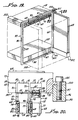
- the connector 10 is hermaphroditic and can mate with an identical connector 10 at its forward end. Each of the mating connectors will be connected to a printed circuit board at its rearward end. A number of printed circuit boards can be interconnected by the arrangement shown in FIGS. 14-21.
- the carrier 68 is an elongated member that includes a longitudinal base wall 70 and a series of equally spaced parallel forward transverse walls 71 which are perpendicular to the base wall.
- a thicker transverse wall 72 is at one end portion of the carrier 68.
- a receptacle 73 which can receive an electrical connector, unlike the connector 10, which forms part of the circuit that supplies power to the printed circuit board attached to the carrier (FIG. 14).
- a similar wall 72 is provided at the opposite end of the carrier 68, but without a receptacle beyond it.
- the transverse walls 71 extend to rearward transverse wall portions 74 of increased thickness. This results in shoulders 75 on either side of each wall 71 at the forward edge of the rearward portion 74. Similar shoulders 76 are defined at the transverse walls 72.
- the carrier 68 in addition, includes an upper wall 77 which extends the length of the unit parallel to the base wall 70 and over the rearward wall portions 74. The upper wall 77 is offset transversely relative to the base wall 70. Therefore, the carrier 68 defines a series of pockets or receptacles between the transverse walls 71 and between the transverse walls 73 which are open at their ends along either side of the carrier, and also open opposite from the walls 70 and 77.
- the rearward transverse wall portions 74 are shorter than the forward transverse walls 71, terminating at bottom edges 78.
- the rearward edge surface 80 of the wall 70 is recessed between adjacent edges.
- One edge portion of the printed circuit board 69 is secured to the carrier 68 by means of screws 81 which extend through a clamping bar 82 and an insulator strip 83, as well as through the printed circuit board 69.
- the screws 81 are received within threaded openings in the rearward wall portions 74.
- Precise alignment of the components is accomplished by pins 84 which extend through the clamping bar 82, the insulator strip 83 and the printed circuit board 69 into the end walls 72 of the carrier 68.
- the printed circuit board 69 then engages the bottom edges 78 of the rearward transverse wall portions 74, and its edge 85 lies alongside the rearwardly facing edge 79 of the carrier 68.
- the printed circuit board 68 includes signal pad arrays 86 spaced adjacent its edge 85 and positioned so that there is one such an array between adjacent wall portions 74, rearwardly of the longitudinal wall 70.
- a grounding field is produced by including grommets 87 around the screws 81, extending through the clamping bar 82, each with a head 88 at an opening in the insulator strip 83.
- a grounding plane 89 is exposed on the underside of the printed circuit board 69 and engaged by the grommet head 88.
- the ground conductor 89 includes openings 89a at its opposite ends so that it extends around two adjacent contact arrays 86. Each adjacent pair of contact arrays 86 is provided with a grounding field in this manner.
- the grounding plane 89 includes two frame portions 89b that extend around the paired contact arrays 86 on the upper side of the printed circuit board 69 and are connected to the lower portion by conductors 89c.
- the grounding contact dots 60 of the flexible circuit 46 engage the frame portions 89b.
- a connector 10 is inserted into each of the pockets in the carrier 68 where a connection is to be made to the printed circuit board 69.
- the rearward portion 13 of the connector housing 11 fits generally complementarily between the two opposed rearward wall sections 74, while the forward portion 12 of the connector housing is confined between the forward transverse walls 71.
- the shoulder 14 between the forward housing portion 12 and the rearward housing portion 13 engages the shoulders 75 and 76 of the carrier 68 as well as the forward edge 90 of the longitudinal wall 77. This limits the travel of the connector 10 into the pocket in the carrier so that the connector 10 then has a predetermined position relative to the carrier. In that position the array of contact stripes 56 faces outwardly along the side of the carrier 68 adjacent the longitudinal base wall 70.
- the other array of contacts 59 of the flexible circuit 46 of the connector faces downwardly, as illustrated, adjacent the opposite side of the carrier.
- the array of contacts 59 is aligned with one of the signal pad contact arrays 86 of the printed circuit board 69.
- Each of the contact dots 59 of the flexible circuit 46 bears against one of the contacts of the printed circuit board, as seen in FIG. 21.
- the grounding contact dots 60 of the flexible circuit engage the upper portion of the frame 89a of the ground conductor 89, which is exposed on one side of the printed circuit board 69.
- the pressure table 35 is biased toward the printed circuit board by the compression springs 44 to accomplish firm engagement and an electrical connection between the contacts of the flexible circuit 46 and those of the printed circuit board 69.
- the resilient pad 50 distributes the spring force so that an electrical connection is assured at each set of mating contacts.
- the clamping bar 82 is tightened into position by the screws 81 only after the connectors 10 are positioned in the pockets in the carrier 68, to permit assembly without damaging the components.
- the separate clamping bar 82 enables the system to accommodate printed circuit boards of different thicknesses.
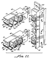
- FIGS. 19 and 20 Connections among various printed circuit boards may be accomplished with the midplane connecting arrangement shown in FIGS. 19 and 20.
- this arrangement there is a rectangular frame 92 which, as illustrated, includes parallel top and bottom rails 93 and 94 and side rails 95 and 96.
- a series of equally spaced threaded openings 97 is provided in the top rail 93 with similar openings formed in the bottom and side rails 94, 95 and 96.
- Each of the carriers 68 is provided with an outwardly projecting flange 100 at either end of the carrier.
- One set of carriers 68, with printed circuit boards 69 attached, is secured to the top and bottom rails 93 and 94 by means of screws 101 that are received in the tapped openings 97.
- a second set of printed circuit boards is attached to the side rails 95 and 96 by means of screws 101 that enter the threaded openings 97 of those rails.
- the result is a set of parallel printed circuit boards 69 which are in a horizontal alignment and are perpendicular to the other set of printed circuit boards.
- each circuit board within the housing 102 along one edge of each circuit board, as shown in FIG. 19, are the power supply wire harnesses for the printed circuit board 69, which may be both electrical and optical. This connects to a power supply module 103.
- grounding clips 61 are provided for the connectors 10 the forwardly projecting flanges 64 and 65 of one grounding clip engage the square base frame of the other. An effective grounding shield is accomplished in this manner.
- Additional or alternative grounding may be accomplished by a conductive gasket 106 positioned along the forward longitudinal edge 107 of the base wall 70 of the carrier 68 at each of the pockets for a connector 10.
- the gaskets 106 engage each other in a cruciform pattern when the two sets of carriers are attached to the frame 92. Only the gaskets of the carriers touch each other; the edges 107 of the carrier 68 do not.
Applications Claiming Priority (2)
| Application Number | Priority Date | Filing Date | Title |
|---|---|---|---|
| US922909 | 1978-07-10 | ||
| US07/922,909 US5248261A (en) | 1992-07-31 | 1992-07-31 | Double ended hermaphroditic signal node module |
Publications (2)
| Publication Number | Publication Date |
|---|---|
| EP0583097A1 true EP0583097A1 (fr) | 1994-02-16 |
| EP0583097B1 EP0583097B1 (fr) | 1997-01-08 |
Family
ID=25447765
Family Applications (1)
| Application Number | Title | Priority Date | Filing Date |
|---|---|---|---|
| EP93305826A Expired - Lifetime EP0583097B1 (fr) | 1992-07-31 | 1993-07-23 | Module hermaphrodite pour noeud de signaux à terminal double |
Country Status (4)
| Country | Link |
|---|---|
| US (1) | US5248261A (fr) |
| EP (1) | EP0583097B1 (fr) |
| JP (1) | JP2529078B2 (fr) |
| DE (1) | DE69307217T2 (fr) |
Cited By (3)
| Publication number | Priority date | Publication date | Assignee | Title |
|---|---|---|---|---|
| EP0938167A1 (fr) * | 1998-02-19 | 1999-08-25 | Japan Aviation Electronics Industry, Limited | Connecteur à angle droit ayant des trajets de signaux avec les mêmes longueurs |
| EP1024554A2 (fr) * | 1999-01-28 | 2000-08-02 | Intercon Systems, Inc. | Système de connecteur à compression et procédé de fabrication |
| WO2007005522A2 (fr) * | 2005-07-05 | 2007-01-11 | Amphenol Corporation | Connecteur electrique de jeu d'echecs |
Families Citing this family (18)
| Publication number | Priority date | Publication date | Assignee | Title |
|---|---|---|---|---|
| US5759047A (en) * | 1996-05-24 | 1998-06-02 | International Business Machines Corporation | Flexible circuitized interposer with apertured member and method for making same |
| US5899757A (en) | 1997-11-03 | 1999-05-04 | Intercon Systems, Inc. | Compression connector |
| US6533588B1 (en) * | 2000-03-30 | 2003-03-18 | Delphi Technologies, Inc. | Connector assembly for flexible circuits |
| US20090316372A1 (en) * | 2008-06-24 | 2009-12-24 | Albert David Kozlovski | Printed circuit board assembly |
| US7794233B1 (en) | 2009-06-09 | 2010-09-14 | Tyco Electronics Corporation | Flexible circuit member for electrically coupling connectors with one another |
| US8033852B2 (en) * | 2009-12-23 | 2011-10-11 | Tyco Electronics Corporation | Connector assembly for coupling circuit boards |
| US9300081B2 (en) * | 2010-02-02 | 2016-03-29 | Charles Albert Rudisill | Interposer connectors with magnetic components |
| US8292644B2 (en) | 2010-04-09 | 2012-10-23 | Tyco Electronics Corporation | Connector assembly having a floating mating array |
| US8251755B2 (en) | 2010-06-14 | 2012-08-28 | Tyco Electronics Corporation | Connector with a laterally moving contact |
| DE102011101767A1 (de) * | 2011-05-17 | 2012-11-22 | Hi-Kabelkonfektionierungs Gmbh | Verbinder zur Herstellung einer elektrischen Kontaktverbindung |
| US10680383B2 (en) | 2013-03-14 | 2020-06-09 | Apex Technologies, Inc. | Linear electrode systems for module attachment with non-uniform axial spacing |
| CN104134903B (zh) * | 2014-07-15 | 2016-05-25 | 深圳市兴森快捷电路科技股份有限公司 | 一种高速连接器与测试单板的连接体、工装及测试方法 |
| DE102016107412A1 (de) * | 2016-04-21 | 2017-10-26 | Phoenix Contact Gmbh & Co. Kg | Steckverbinderteil mit in einen Halterahmen eingesetzten modularen Kontakteinsätzen |
| JP6909304B2 (ja) * | 2016-11-16 | 2021-07-28 | セント・ジュード・メディカル,カーディオロジー・ディヴィジョン,インコーポレイテッド | 医療機器用の大容量コネクタ |
| US10615530B2 (en) | 2017-06-06 | 2020-04-07 | Amphenol Corporation | Spring loaded electrical connector |
| US10050367B1 (en) * | 2017-06-06 | 2018-08-14 | Amphenol Corporation | Spring loaded electrical connector |
| WO2020159816A1 (fr) * | 2019-01-30 | 2020-08-06 | Amphenol Corporation | Connecteur électrique à ressort |
| DE102020121222A1 (de) | 2020-08-12 | 2022-02-17 | Deutsches Zentrum für Luft- und Raumfahrt e.V. | Hermaphroditischer Stecker |
Citations (3)
| Publication number | Priority date | Publication date | Assignee | Title |
|---|---|---|---|---|
| EP0145083A2 (fr) * | 1983-12-02 | 1985-06-19 | E.I. Du Pont De Nemours And Company | Connecteur électrique utilisant un circuit flexible à dispositif de contrôle d'impédance |
| US5161986A (en) * | 1991-10-15 | 1992-11-10 | Ceridian Corporation | Low inductance circuit apparatus with controlled impedance cross-unders and connector for connecting to backpanels |
| US5199881A (en) * | 1991-12-03 | 1993-04-06 | Hughes Aircraft Company | Hermaphroditic interconnection of circuit boards |
Family Cites Families (5)
| Publication number | Priority date | Publication date | Assignee | Title |
|---|---|---|---|---|
| US3065446A (en) * | 1958-09-29 | 1962-11-20 | Cannon Electric Co | Electrical connector for strip cable |
| US4871315A (en) * | 1988-03-30 | 1989-10-03 | Burndy Corporation | Ribbon cable connector |
| US4881901A (en) * | 1988-09-20 | 1989-11-21 | Augat Inc. | High density backplane connector |
| US4907975A (en) * | 1988-12-19 | 1990-03-13 | International Business Machine Corporation | Electrical connector utilizing flexible electrical circuitry |
| US4950171A (en) * | 1989-08-11 | 1990-08-21 | Itt Corporation | Fuel injector connector system |
-
1992
- 1992-07-31 US US07/922,909 patent/US5248261A/en not_active Expired - Fee Related
-
1993
- 1993-07-23 EP EP93305826A patent/EP0583097B1/fr not_active Expired - Lifetime
- 1993-07-23 DE DE69307217T patent/DE69307217T2/de not_active Expired - Fee Related
- 1993-08-02 JP JP5191449A patent/JP2529078B2/ja not_active Expired - Lifetime
Patent Citations (3)
| Publication number | Priority date | Publication date | Assignee | Title |
|---|---|---|---|---|
| EP0145083A2 (fr) * | 1983-12-02 | 1985-06-19 | E.I. Du Pont De Nemours And Company | Connecteur électrique utilisant un circuit flexible à dispositif de contrôle d'impédance |
| US5161986A (en) * | 1991-10-15 | 1992-11-10 | Ceridian Corporation | Low inductance circuit apparatus with controlled impedance cross-unders and connector for connecting to backpanels |
| US5199881A (en) * | 1991-12-03 | 1993-04-06 | Hughes Aircraft Company | Hermaphroditic interconnection of circuit boards |
Cited By (6)
| Publication number | Priority date | Publication date | Assignee | Title |
|---|---|---|---|---|
| EP0938167A1 (fr) * | 1998-02-19 | 1999-08-25 | Japan Aviation Electronics Industry, Limited | Connecteur à angle droit ayant des trajets de signaux avec les mêmes longueurs |
| US6171139B1 (en) | 1998-02-19 | 2001-01-09 | Japan Aviation Electronics Industry, Limited | Right-angle connector unit having signal passes equal to one another in length |
| EP1024554A2 (fr) * | 1999-01-28 | 2000-08-02 | Intercon Systems, Inc. | Système de connecteur à compression et procédé de fabrication |
| EP1024554A3 (fr) * | 1999-01-28 | 2000-10-04 | Intercon Systems, Inc. | Système de connecteur à compression et procédé de fabrication |
| WO2007005522A2 (fr) * | 2005-07-05 | 2007-01-11 | Amphenol Corporation | Connecteur electrique de jeu d'echecs |
| WO2007005522A3 (fr) * | 2005-07-05 | 2007-05-10 | Amphenol Corp | Connecteur electrique de jeu d'echecs |
Also Published As
| Publication number | Publication date |
|---|---|
| JP2529078B2 (ja) | 1996-08-28 |
| EP0583097B1 (fr) | 1997-01-08 |
| DE69307217D1 (de) | 1997-02-20 |
| US5248261A (en) | 1993-09-28 |
| JPH06163126A (ja) | 1994-06-10 |
| DE69307217T2 (de) | 1997-05-07 |
Similar Documents
| Publication | Publication Date | Title |
|---|---|---|
| EP0583097B1 (fr) | Module hermaphrodite pour noeud de signaux à terminal double | |
| KR960002136B1 (ko) | 접지 구조물을 갖고 있는 커넥터 | |
| EP0317925B1 (fr) | Clip et plaque de terre pour une fiche de contact | |
| US5308252A (en) | Interposer connector and contact element therefore | |
| KR940011264B1 (ko) | 접지 구조물을 갖고 있는 커넥터 | |
| EP0854549B1 (fr) | Connecteur pour le montage sur une surface avec assemblage intégré de circuit imprimé | |
| US5334046A (en) | Circuit card interface system | |
| US5358411A (en) | Duplex plated epsilon compliant beam contact and interposer | |
| US5055069A (en) | Connectors with ground structure | |
| US5026292A (en) | Card edge connector | |
| US6705895B2 (en) | Orthogonal interface for connecting circuit boards carrying differential pairs | |
| US7771207B2 (en) | Assembly for interconnecting circuit boards | |
| US5306171A (en) | Bowtie connector with additional leaf contacts | |
| US5106311A (en) | Connector | |
| EP0764392B1 (fr) | Ensemble rail | |
| US11264765B2 (en) | Electrical connector and electrical connector assembly | |
| WO2003081726A1 (fr) | Connecteur modulaire a interconnexion de mise a la terre | |
| CA1219315A (fr) | Dispositif d'auto-correspondance de contacts electriques | |
| US5785534A (en) | Electrical connector | |
| JPH06208874A (ja) | カードリーダ用電気コネクタ | |
| US7059907B2 (en) | Modular electrical connector | |
| JPS61248375A (ja) | 電気コネクタ | |
| US7438556B2 (en) | Electrical interconnection between multiple printed circuit boards | |
| US6472599B2 (en) | Arrangement for supplying power from a buss bar to a circuit board | |
| CN2313311Y (zh) | 电连接器 |
Legal Events
| Date | Code | Title | Description |
|---|---|---|---|
| PUAI | Public reference made under article 153(3) epc to a published international application that has entered the european phase |
Free format text: ORIGINAL CODE: 0009012 |
|
| AK | Designated contracting states |
Kind code of ref document: A1 Designated state(s): DE FR GB |
|
| 17P | Request for examination filed |
Effective date: 19940720 |
|
| 17Q | First examination report despatched |
Effective date: 19950428 |
|
| GRAG | Despatch of communication of intention to grant |
Free format text: ORIGINAL CODE: EPIDOS AGRA |
|
| GRAH | Despatch of communication of intention to grant a patent |
Free format text: ORIGINAL CODE: EPIDOS IGRA |
|
| GRAH | Despatch of communication of intention to grant a patent |
Free format text: ORIGINAL CODE: EPIDOS IGRA |
|
| GRAA | (expected) grant |
Free format text: ORIGINAL CODE: 0009210 |
|
| AK | Designated contracting states |
Kind code of ref document: B1 Designated state(s): DE FR GB |
|
| REF | Corresponds to: |
Ref document number: 69307217 Country of ref document: DE Date of ref document: 19970220 |
|
| ET | Fr: translation filed | ||
| PGFP | Annual fee paid to national office [announced via postgrant information from national office to epo] |
Ref country code: FR Payment date: 19970613 Year of fee payment: 5 |
|
| PGFP | Annual fee paid to national office [announced via postgrant information from national office to epo] |
Ref country code: GB Payment date: 19970620 Year of fee payment: 5 |
|
| PGFP | Annual fee paid to national office [announced via postgrant information from national office to epo] |
Ref country code: DE Payment date: 19970623 Year of fee payment: 5 |
|
| PLBE | No opposition filed within time limit |
Free format text: ORIGINAL CODE: 0009261 |
|
| STAA | Information on the status of an ep patent application or granted ep patent |
Free format text: STATUS: NO OPPOSITION FILED WITHIN TIME LIMIT |
|
| 26N | No opposition filed | ||
| PG25 | Lapsed in a contracting state [announced via postgrant information from national office to epo] |
Ref country code: GB Free format text: LAPSE BECAUSE OF NON-PAYMENT OF DUE FEES Effective date: 19980723 |
|
| GBPC | Gb: european patent ceased through non-payment of renewal fee |
Effective date: 19980723 |
|
| PG25 | Lapsed in a contracting state [announced via postgrant information from national office to epo] |
Ref country code: FR Free format text: LAPSE BECAUSE OF NON-PAYMENT OF DUE FEES Effective date: 19990331 |
|
| PG25 | Lapsed in a contracting state [announced via postgrant information from national office to epo] |
Ref country code: DE Free format text: LAPSE BECAUSE OF NON-PAYMENT OF DUE FEES Effective date: 19990501 |
|
| REG | Reference to a national code |
Ref country code: FR Ref legal event code: ST |