EP0579025A2 - Digital-analog converter with weighted capacitive network - Google Patents
Digital-analog converter with weighted capacitive network Download PDFInfo
- Publication number
- EP0579025A2 EP0579025A2 EP93110323A EP93110323A EP0579025A2 EP 0579025 A2 EP0579025 A2 EP 0579025A2 EP 93110323 A EP93110323 A EP 93110323A EP 93110323 A EP93110323 A EP 93110323A EP 0579025 A2 EP0579025 A2 EP 0579025A2
- Authority
- EP
- European Patent Office
- Prior art keywords
- network
- converter
- weighted
- stray capacitances
- capacitances
- Prior art date
- Legal status (The legal status is an assumption and is not a legal conclusion. Google has not performed a legal analysis and makes no representation as to the accuracy of the status listed.)
- Granted
Links
Images

Classifications
-
- H—ELECTRICITY
- H03—ELECTRONIC CIRCUITRY
- H03M—CODING; DECODING; CODE CONVERSION IN GENERAL
- H03M1/00—Analogue/digital conversion; Digital/analogue conversion
- H03M1/06—Continuously compensating for, or preventing, undesired influence of physical parameters
- H03M1/08—Continuously compensating for, or preventing, undesired influence of physical parameters of noise
- H03M1/0863—Continuously compensating for, or preventing, undesired influence of physical parameters of noise of switching transients, e.g. glitches
-
- H—ELECTRICITY
- H03—ELECTRONIC CIRCUITRY
- H03M—CODING; DECODING; CODE CONVERSION IN GENERAL
- H03M1/00—Analogue/digital conversion; Digital/analogue conversion
- H03M1/06—Continuously compensating for, or preventing, undesired influence of physical parameters
- H03M1/0617—Continuously compensating for, or preventing, undesired influence of physical parameters characterised by the use of methods or means not specific to a particular type of detrimental influence
- H03M1/0675—Continuously compensating for, or preventing, undesired influence of physical parameters characterised by the use of methods or means not specific to a particular type of detrimental influence using redundancy
- H03M1/0678—Continuously compensating for, or preventing, undesired influence of physical parameters characterised by the use of methods or means not specific to a particular type of detrimental influence using redundancy using additional components or elements, e.g. dummy components
- H03M1/068—Continuously compensating for, or preventing, undesired influence of physical parameters characterised by the use of methods or means not specific to a particular type of detrimental influence using redundancy using additional components or elements, e.g. dummy components the original and additional components or elements being complementary to each other, e.g. CMOS
- H03M1/0682—Continuously compensating for, or preventing, undesired influence of physical parameters characterised by the use of methods or means not specific to a particular type of detrimental influence using redundancy using additional components or elements, e.g. dummy components the original and additional components or elements being complementary to each other, e.g. CMOS using a differential network structure, i.e. symmetrical with respect to ground
-
- H—ELECTRICITY
- H03—ELECTRONIC CIRCUITRY
- H03M—CODING; DECODING; CODE CONVERSION IN GENERAL
- H03M1/00—Analogue/digital conversion; Digital/analogue conversion
- H03M1/66—Digital/analogue converters
- H03M1/74—Simultaneous conversion
- H03M1/80—Simultaneous conversion using weighted impedances
- H03M1/802—Simultaneous conversion using weighted impedances using capacitors, e.g. neuron-mos transistors, charge coupled devices
- H03M1/804—Simultaneous conversion using weighted impedances using capacitors, e.g. neuron-mos transistors, charge coupled devices with charge redistribution
Definitions
- the invention relates to a digital-to-analog converter with a weighted capacitive converter network.
- Capacitive digital-to-analog converters have long been known, for example from D. Seitzer's book: “Electronic Analog-to-Digital Converter", Springer-Verlag, Berlin, 1977, page 82 f.
- a switch controlled by digital information charges a capacitance in a first clock period.
- the switch is opened and a further capacitor is connected in parallel via a further switch, so that the charge stored in the first cycle period is distributed over both capacities.
- the switch and capacitance can be replaced by a switch network and a weighted capacitive network.
- Basic principles of weighted networks for D / A converters are known, for example, from U. Tietze, Ch. Schenk: “Semiconductor circuit technology", Springer-Verlag, Berlin, 7th edition, 1985, page 739 ff.
- a D / A converter based on the principle of charge redistribution with a weighted capacitive network is followed by a continuous-time interpolation filter, ie a low-pass filter, in certain applications. Due to the continuous-time filter, the output voltage of the digital-to-analog converter is evaluated continuously, ie at all times. The transient response of the converter thus has a significant influence on the conversion result that can be achieved. Basically, the goal is to convert one and the same digital code at the output of the continuous time Filters get an analog value that corresponds exactly to the digital code.
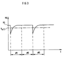
- the output voltage assigned to a digital code can be falsified due to switching peaks in the switches of the converter, as is schematically explained in FIG. 3.
- the setpoint of the output voltage VS breaks down briefly at the beginning of each first clock period ⁇ 1, which controls the weighted network, and then reaches the setpoint.
- the signal curve results in an effective output voltage V eff that is lower than the target output voltage V S.
- this phenomenon of switching peaks occurs particularly disruptively during transitions from one code to the next when several or many elements of the code change. This is the case, for example, when changing from code 01111 to code 10000. This is due to the fact that said switching peaks are strongly correlated with the individual bits. If many bits are changed, the switching tip also changes significantly. Overall, the parasitic effect results in a strong non-linearity in the characteristic curve of the D / A converter.
- a D / A converter with an undivided capacitive network will typically have an improved linearity characteristic.
- the use of an undivided capacitive network also means the use of larger capacities, which in turn means a dramatic increase in the chip area required.
- the invention has for its object to provide a digital-to-analog converter with a weighted capacitive converter network, which has a low power consumption and a good linearity characteristic with a small chip area required.
- Embodiments of the invention are characterized in the subclaims.
- FIG. 1 shows a block diagram of a digital-to-analog converter according to the invention.
- the converter is completely differential. This means that the circuitry of an operational amplifier OPA is symmetrical with regard to the inverting and non-inverting connections.
- the operational amplifier is connected to four capacitors C1 to C4 and two converter networks CN1 and CN2.
- the capacities C1 and C3 as well as C2 and C4 are the same.
- the arrangement works with a two-phase clock ⁇ 1 and ⁇ 2, which is generated by a clock generator, not shown.
- Input variables for the capacitance networks are the reference potentials REF1 and REF2, a reference potential VB and a control bus BST, which contains the digital information to be converted.
- the capacitance networks and the switches S1 to S4 are controlled by the clocks ⁇ 1 and ⁇ 2.
- the circuitry for the inverting input - and the non-inverted output + of the operational amplifier OPA provides the capacitance C1 between these two connections.
- the inverting input is also connected at clock ⁇ 2 via switch S1 to node CT1 of capacitance network CN1 and via switch S3 to capacitance C3.
- the capacitance C3 is with her other Connection connected to the inverted output 02 of the operational amplifier.
- the switches S1 and S3 are connected to the reference potential VB, so that the capacitance C3 and the node CT1 of the capacitance network CN1 are connected to the reference potential.
- the non-inverted output + of the operational amplifier OPA is connected to the output connection 01 and a connection of the capacitance network CN1.
- the non-inverting input + and the inverted output - of the operational amplifier OPA according to FIG. 1 are connected in a corresponding manner.
- the capacitance networks CN1 and CN2 are charged to the reference potentials REF1, REF2 and VB in accordance with the digital code present.
- These reference potentials can be the positive and negative input reference voltages, for example, if the reference potential VB is the ground potential.
- outputs 01 and 02 of the operational amplifier retain the same values as in the previous clock period. Capacitors C3 and C4 are therefore charged to the output potentials of outputs 01 and 02.
- the charges stored on the capacitance networks CN1 and CN2 are therefore not redistributed, so that the output connections 01 and 02 assume the analog voltage value that corresponds to the last digital input signal for the capacitance networks during the clock ⁇ 1. It should be added that the capacitance values can be chosen to be very low because they are limited only by the accuracy of the compensation between C1 and C3 or C2 and C4.
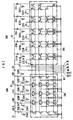
- FIG. 2 shows one of the two capacity networks in detail.
- Each capacity network contains a main network CNH and a partial or split network CNS.
- the two network parts are connected to one another via a coupling capacitance CK.
- Each sub-network contains weighted capacities CH1 to CH16 or CS1 to CS16.
- the network arrangement represents only one example of the invention. Of course, the capacities can also be divided differently between the subnetworks, or only an undivided network can be provided even without a subnetwork.
- the capacitances CHi of the main network are each connected to a connection at a common node K1 or to the connection CT. With their respective other connection, the weighted capacities of the main network are connected to a switch network SNH.
- the weighted capacitances CSi of the split network CNS are each connected to a second common node K2, which can be connected to the reference potential VB via a switch clocked by the clock ⁇ 1. This switch can also be omitted.
- the coupling capacitance CK lies between the two nodes K1 and K2.
- the other connections of the weighted capacities of the split network are connected to an associated switch network SNS.
- each switch network has four switch levels.
- the switches of three switch levels are controlled via the control bus BST, so that depending on the digital code applied, one of the potentials REF1, REF2 or VB can be connected to the associated connection of one of the weighted capacities of the main network or the split network.
- the fourth switch level is controlled by the clock ⁇ 2 and can connect the associated output 01 or 02 of the operational amplifier OPA to the respective connection of the weighted capacitors.
- the nodes K1 and K2 can be connected via the connection CT to one of the input connections of the operational amplifier or to the reference potential VB, as is described in FIG. 1.
- FIG. 2 also shows stray capacitances SCH1 to SCH16 for the main network CNH and stray capacities SCS1 to SCS16 for the split network CNS.
- These stray capacities result, for example, from the wiring or the technological structure of the useful capacities.
- the stray capacitances of the capacitance networks are charged either to a reference potential or to the reference potential VB.
- the stray capacitances must be reloaded to the final analog output voltages of the operational amplifier.
- the operational amplifier OPA has to provide the necessary power.
- the invention starts with the knowledge that the non-linearities described in connection with FIG. 3 are largely due to the stray capacitances.
- the invention therefore provides for additional scattering capacities to be arranged parallel to the existing scattering capacities, that the total stray capacities are weighted. With such stray capacitances weighted according to the useful capacities, the effective charge of all parasitic stray capacitances is then proportional to the output voltage at the output connections of the operational amplifier. Furthermore, an optimal coordination of the time constants from the respective switch resistance and the associated stray capacitance is possible. Because the effective charge of all stray capacitances is proportional to the output voltage, only a gain error can result, since the transient response is matched to the respective digital code.
- the teaching of the invention means that the parasitic capacitances must also be binary-weighted. This is usually not the case. This disparity between the main and the split network is usually particularly severe.
- One embodiment of the teaching according to the invention provides for the correct weighting of the parasitic stray capacitances to be achieved by connecting additional parasitic capacitances in parallel with the already existing stray capacitances until a corresponding, for example binary, weighting is achieved.
- Figure 2 shows the additional stray capacities CSA1 and CSA2 of the network SNH. Usually, the stray capacity of the least significant bit LSB is assumed. The parasitic capacitances of the higher-order bits are then doubled from stage to stage. However, since the stray capacitance of the least significant bit LSB is usually relatively large, this procedure also requires that of the stray capacitors provided in the arrangement according to FIG. 1 due to the gradual doubling of the stray capacitances low capacities overall comparatively high capacities and thus a large chip area
- the stray capacitance of a higher-value bit is assumed and the stray capacitance of the lower-weighted bits is reduced in accordance with the required weighting.
- This is made possible by providing the stray capacitances of the lower order bits with effective, i.e. negative capacitance is connected in parallel during the second clock period.
- a parallel connection of a negative effective capacitance is realized by connecting a capacitance with parallel-phase control in parallel.
Abstract
Description
Die Erfindung betrifft einen Digital-Analog-Wandler mit einem gewichteten kapazitiven Wandlernetzwerk.The invention relates to a digital-to-analog converter with a weighted capacitive converter network.
Kapazitive Digital-Analog-Wandler sind seit langem bekannt, beispielsweise aus dem Buch von D. Seitzer: "Elektronische Analog-Digital-Umsetzer", Springer-Verlag, Berlin, 1977, Seite 82 f. Ein von einer digitalen Information gesteuerter Schalter lädt in einer ersten Taktperiode eine Kapazität auf. Während einer zweiten Taktperiode wird der Schalter geöffnet und über einen weiteren Schalter eine weitere Kapazität parallelgeschaltet, so daß sich die in der ersten Taktperiode gespeicherte Ladung auf beide Kapazitäten verteilt. Der Schalter und die Kapazität können durch ein Schalternetzwerk und ein gewichtetes kapazitives Netzwerk ersetzt werden. Grundprinzipien gewichteter Netze für D/A-Wandler sind beispielsweise aus U. Tietze, Ch. Schenk: "Halbleiter-Schaltungstechnik", Springer-Verlag, Berlin, 7. Aufl., 1985, Seite 739 ff. bekannt.Capacitive digital-to-analog converters have long been known, for example from D. Seitzer's book: "Electronic Analog-to-Digital Converter", Springer-Verlag, Berlin, 1977, page 82 f. A switch controlled by digital information charges a capacitance in a first clock period. During a second cycle period, the switch is opened and a further capacitor is connected in parallel via a further switch, so that the charge stored in the first cycle period is distributed over both capacities. The switch and capacitance can be replaced by a switch network and a weighted capacitive network. Basic principles of weighted networks for D / A converters are known, for example, from U. Tietze, Ch. Schenk: "Semiconductor circuit technology", Springer-Verlag, Berlin, 7th edition, 1985, page 739 ff.
Einem D/A-Wandler nach dem Prinzip der Ladungsumverteilung mit gewichtetem kapazitiven Netzwerk wird bei bestimmten Anwendungen ein zeitkontinuierliches Interpolationsfilter, d.h. ein Tiefpaß nachgeschaltet. Aufgrund des zeitkontinuierlichen Filters wird die Ausgangsspannung des Digital-Analog-Wandlers zeitkontinuierlich, d.h. zu allen Zeiten bewertet. Damit hat das Einschwingverhalten des Wandlers einen wesentlichen Einfluß auf das erzielbare Wandlungsergebnis. Grundsätzlich besteht das Ziel, bei der Wandlung ein und derselben Digitalcodes am Ausgang des zeitkontinuierlichen Filters einen Analogwert zu erhalten, der genau dem Digitalcode entspricht.A D / A converter based on the principle of charge redistribution with a weighted capacitive network is followed by a continuous-time interpolation filter, ie a low-pass filter, in certain applications. Due to the continuous-time filter, the output voltage of the digital-to-analog converter is evaluated continuously, ie at all times. The transient response of the converter thus has a significant influence on the conversion result that can be achieved. Basically, the goal is to convert one and the same digital code at the output of the continuous time Filters get an analog value that corresponds exactly to the digital code.
In der Praxis jedoch kann die einem Digitalcode zugeordnete Ausgangsspannung aufgrund von Schaltspitzen der Schalter des Wandlers verfälscht sein, wie dies Figur 3 schematisch erläutert. Der Sollwert der Ausgangsspannung VS bricht zu Beginn jeder ersten Taktperiode φ1, die das gewichtete Netzwerk steuert, kurzzeitig zusammen und erreicht dann den Sollwert. Aus dem Signalverlauf ergibt sich eine gegenüber der Soll-Ausgangsspannung VS verringerte effektive Ausgangsspannung Veff.In practice, however, the output voltage assigned to a digital code can be falsified due to switching peaks in the switches of the converter, as is schematically explained in FIG. 3. The setpoint of the output voltage VS breaks down briefly at the beginning of each first clock period φ1, which controls the weighted network, and then reaches the setpoint. The signal curve results in an effective output voltage V eff that is lower than the target output voltage V S.
In einem Wandler der geschilderten Art tritt dieses Phänomen der Schaltspitzen besonders störend bei Übergängen von einem Code zum nächsten dann auf, wenn sich mehrere oder viele Elemente des Codes ändern. Dies ist beispielsweise beim Übergang von einem Code 01111 zu einem Code 10000 der Fall. Dies ist dadurch begründet, daß besagte Schaltspitzen stark mit den einzelnen Bits korreliert sind. Bei Änderung vieler Bits ändert sich auch die Schaltspitze stark. Insgesamt ergibt der parasitäre Effekt eine starke Nichtlinearität in der Kennlinie des D/A-Wandlers.In a converter of the type described, this phenomenon of switching peaks occurs particularly disruptively during transitions from one code to the next when several or many elements of the code change. This is the case, for example, when changing from code 01111 to code 10000. This is due to the fact that said switching peaks are strongly correlated with the individual bits. If many bits are changed, the switching tip also changes significantly. Overall, the parasitic effect results in a strong non-linearity in the characteristic curve of the D / A converter.
Grundsätzlich ist es schwierig, Nichtlinearitäten völlig zu vermeiden. Wünschenswert ist aber eine Kennlinie mit einer Form, die eine gute Linearität ermöglicht. Andere Kennlinienstörungen, wie etwa ein Verstärkungsfehler, spielen bei D/A-Wandlern wie auch bei den meisten nachrichtentechnischen Anwendungen keine so große Rolle wie Nichtlinearitäten.Basically, it is difficult to completely avoid non-linearities. However, a characteristic curve with a shape that enables good linearity is desirable. Other characteristic curve disturbances, such as a gain error, do not play as great a role in D / A converters as in most communication technology applications, like non-linearities.
In integrierten D/A-Wandlern wird oft das Wandlernetzwerk in zwei kapazitive Teilnetzwerke aufgespalten, die über eine Koppelkapazität verbunden sind. Ein D/A-Wandler mit einem ungeteilten kapazitiven Netzwerk wird typischerweise eine verbesserte Linearitätskennlinie besitzen. Die Verwendung eines ungeteilten kapazitiven Netzwerkes bedeutet aber die Verwendung auch größerer Kapazitäten, die wiederum eine dramatische Vergrößerung der benötigten Chipfläche bedeuten.In integrated D / A converters, the converter network is often split into two capacitive sub-networks, which are connected via a coupling capacitance. A D / A converter with an undivided capacitive network will typically have an improved linearity characteristic. The use of an undivided capacitive network also means the use of larger capacities, which in turn means a dramatic increase in the chip area required.
Eine weitere Möglichkeit zur Verbesserung der Linearitätskennlinie besteht darin, die Einschwingzeit zu verkürzen. Dann wird die Zeit, in der ein gestörtes Signal anliegt, minimiert, wie dies aus Figur 3 zu erklären ist. Allerdings benötigt ein derartiger Lösungsweg wesentlich mehr Leistung als das entsprechende ursprüngliche Wandlungssystem. Besonders bei schnellen Wandlern kann darüberhinaus dieser Weg nicht realisierbar sein.Another way to improve the linearity characteristic is to shorten the settling time. Then the time during which a disturbed signal is present is minimized, as can be explained from FIG. 3. However, such a solution requires much more power than the corresponding original conversion system. In addition, this path cannot be feasible, particularly with fast converters.
Schließlich ist es zur Verbesserung des Linearitätsverhaltens auch möglich, dem D/A-Wandler und dem nachgeschalteten Filter ein Abtast- und Halteglied nachzuschalten, das den Sollwert des Wandlers ab tastet und während der Zeit konstant hält, in der Schaltspitzen auftreten können. Diese Lösungsmöglichkeit bedeutet jedoch einen erheblichen schaltungstechnischen Aufwand, da das Abtast- und Halteglied zusätzlich integriert werden muß.Finally, in order to improve the linearity behavior, it is also possible to connect the D / A converter and the downstream filter with a sample and hold element, which samples the setpoint of the converter and keeps it constant during the time in which switching peaks can occur. However, this possibility of solution means a considerable outlay in terms of circuitry, since the sample and hold element also has to be integrated.
Der Erfindung liegt die Aufgabe zugrunde, einen Digital-Analog-Wandler mit gewichtetem kapazitiven Wandlernetzwerk anzugeben, der bei geringer benötigter Chipfläche eine niedrige Leistungsaufnahme und gute Linearitätskennlinie aufweist.The invention has for its object to provide a digital-to-analog converter with a weighted capacitive converter network, which has a low power consumption and a good linearity characteristic with a small chip area required.
Diese Aufgabe wird mit den Merkmalen der Patentansprüche 1 und 10 gelöst.This object is achieved with the features of
Ausgestaltungen der Erfindung sind in Unteransprüchen gekennzeichnet.Embodiments of the invention are characterized in the subclaims.
Die Erfindung wird nachfolgend anhand der Figuren der Zeichnung näher erläutert. Es zeigen:
Figur 1- ein Blockschaltbild des Digital-Analog-Wandlers,
Figur 2- eine detaillierte Schaltung des beanspruchten Wandlernetzwerks und
- Figur 3
- Diagramme zur Erläuterung des der Erfindung zugrundeliegenden Problems.
- Figure 1
- a block diagram of the digital-to-analog converter,
- Figure 2
- a detailed circuit of the claimed converter network and
- Figure 3
- Diagrams for explaining the problem on which the invention is based.
Figur 1 zeigt als Blockschaltbild einen erfindungsgemäßen Digital-Analog-Wandler. Der Wandler ist vollständig differentiell aufgebaut. Das bedeutet, daß die Beschaltung eines Operationsverstärkers OPA bezüglich der invertierenden und nichtinvertierenden Anschlüsse symmetrisch ist. Der Operationsverstärker ist mit vier Kapazitäten C1 bis C4 und zwei Wandlernetzwerken CN1 und CN2 beschaltet. Die Kapazitäten C1 und C3 sowie C2 und C4 sind jeweils gleich. Die Anordnung arbeitet mit einem zweiphasigen Takt φ1 und φ2, der von einem nicht dargestellten Taktgenerator erzeugt wird. Eingangsgrößen für die Kapazitätsnetzwerke sind die Referenzpotentiale REF1 sowie REF2, ein Bezugspotential VB und ein Steuerbus BST, der die zu wandelnde digitale Information enthält. Die Kapazitätsnetzwerke und die Schalter S1 bis S4 werden von den Takten φ1 und φ2 gesteuert.Figure 1 shows a block diagram of a digital-to-analog converter according to the invention. The converter is completely differential. This means that the circuitry of an operational amplifier OPA is symmetrical with regard to the inverting and non-inverting connections. The operational amplifier is connected to four capacitors C1 to C4 and two converter networks CN1 and CN2. The capacities C1 and C3 as well as C2 and C4 are the same. The arrangement works with a two-phase clock φ1 and φ2, which is generated by a clock generator, not shown. Input variables for the capacitance networks are the reference potentials REF1 and REF2, a reference potential VB and a control bus BST, which contains the digital information to be converted. The capacitance networks and the switches S1 to S4 are controlled by the clocks φ1 and φ2.
Die Beschaltung für den invertierenden Eingang - und den nichtinvertierten Ausgang + des Operationsverstärkers OPA sieht zwischen diesen beiden Anschlüssen die Kapazität C1 vor. Der invertierende Eingang ist weiterhin beim Takt φ2 über den Schalter S1 mit dem Knotenpunkt CT1 des Kapazitätsnetzwerks CN1 verbunden und über den Schalter S3 mit der Kapazität C3. Die Kapazität C3 ist mit ihrem anderen Anschluß am invertierten Ausgang 02 des Operationsverstärkers angeschlossen. Beim Takt φ1 sind die Schalter S1 und S3 mit dem Bezugspotential VB verbunden, so daß die Kapazität C3 und der Knotenpunkt CT1 des Kapazitätsnetzwerks CN1 mit dem Bezugspotential verbunden sind. Der nichtinvertierte Ausgang + des Operationsverstärkers OPA ist an den Ausgangsanschluß 01 und einen Anschluß des Kapazitätsnetzwerks CN1 angeschlossen. In entsprechender Weise sind der nichtinvertierende Eingang + und der invertierte Ausgang - des Operationsverstärkers OPA gemäß Figur 1 beschaltet.The circuitry for the inverting input - and the non-inverted output + of the operational amplifier OPA provides the capacitance C1 between these two connections. The inverting input is also connected at clock φ2 via switch S1 to node CT1 of capacitance network CN1 and via switch S3 to capacitance C3. The capacitance C3 is with her other Connection connected to the inverted
Während des Takts φ1 werden die Kapazitätsnetzwerke CN1 und CN2 entsprechend des anliegenden Digitalcodes auf die Referenzpotentiale REF1, REF2 und VB aufgeladen. Diese Referenzpotentiale können beispielsweise die positive und negative Eingangsreferenzspannung sein, wenn das Bezugspotential VB das Massepotential ist. Gleichzeitig behalten mit dem Takt φ1 die Ausgänge 01 und 02 des Operationsverstärkers dieselben Werte wie in der vorausgegangenen Taktperiode. Die Kapazitäten C3 und C4 werden deshalb auf die Ausgangspotentiale der Ausgänge 01 und 02 geladen.During the clock φ1, the capacitance networks CN1 and CN2 are charged to the reference potentials REF1, REF2 and VB in accordance with the digital code present. These reference potentials can be the positive and negative input reference voltages, for example, if the reference potential VB is the ground potential. At the same time with clock φ1,
Während des Takts φ2 wird jeweils ein Anschluß der Kapazitäten C4 und C3 über den Schalter S4 bzw. S3 an den nichtinvertierenden bzw. invertierenden Eingang des Operationsverstärkers gelegt. Als Konsequenz dieser Rückkopplung folgt, daß die Ladungen auf den Kapazitäten C3 bzw. C4 die Ladungen auf den Kapazitäten C1 bzw. C2 kompensieren. Gleichzeitig erfolgt eine neue Ladungsumverteilung zwischen den Kapazitäten C1 und C3 bzw. C2 und C4, wenn die Kapazitätsnetzwerke CN1 und CN2 über die Schalter S1 und S2 in den Rückkopplungspfad geschaltet werden. Die auf den Kapazitätsnetzwerken CN1 und CN2 gespeicherten Ladungen werden deshalb nicht umverteilt, so daß die Ausgangsanschlüsse 01 und 02 den analogen Spannungswert annehmen, der dem letzten digitalen Eingangssignal für die Kapazitätsnetzwerke während des Takts φ1 entspricht. Es ist hinzuzufügen, daß die Kapazitätswerte sehr niedrig gewählt werden können, weil sie allein durch die Genauigkeit der Kompensation zwischen C1 und C3 bzw. C2 und C4 begrenzt sind.During the clock φ2, a connection of the capacitances C4 and C3 is made via the switches S4 and S3 to the non-inverting or inverting input of the operational amplifier. As a consequence of this feedback it follows that the charges on the capacitors C3 and C4 compensate for the charges on the capacitors C1 and C2. At the same time, a new charge redistribution takes place between the capacitances C1 and C3 or C2 and C4 if the capacitance networks CN1 and CN2 are switched into the feedback path via the switches S1 and S2. The charges stored on the capacitance networks CN1 and CN2 are therefore not redistributed, so that the
Figur 2 zeigt eines der beiden Kapazitätsnetzwerke im Detail. Jedes Kapazitätsnetzwerk enthält ein Hauptnetzwerk CNH und ein Teil- oder Split-Netzwerk CNS. Die beiden Netzwerksteile sind über eine Koppelkapazität CK miteinander verbunden. Jedes Teilnetzwerk enthält gewichtete Kapazitäten CH1 bis CH16 bzw. CS1 bis CS16. Die Netzwerksanordnung stellt nur ein Beispiel der Erfindung dar. Selbstverständlich können die Kapazitäten auch anders auf die Teilnetzwerke aufgeteilt sein, oder es kann auch ohne Teilnetzwerk nur ein ungeteiltes Netzwerk vorgesehen sein. Die Kapazitäten CHi des Hauptnetzwerks sind mit jeweils einem Anschluß an einem gemeinsamen Knotenpunkt K1 bzw. an dem Anschluß CT angeschlossen. Mit ihrem jeweils anderen Anschluß sind die gewichteten Kapazitäten des Hauptnetzwerks mit einem Schalternetzwerk SNH verbunden.Figure 2 shows one of the two capacity networks in detail. Each capacity network contains a main network CNH and a partial or split network CNS. The two network parts are connected to one another via a coupling capacitance CK. Each sub-network contains weighted capacities CH1 to CH16 or CS1 to CS16. The network arrangement represents only one example of the invention. Of course, the capacities can also be divided differently between the subnetworks, or only an undivided network can be provided even without a subnetwork. The capacitances CHi of the main network are each connected to a connection at a common node K1 or to the connection CT. With their respective other connection, the weighted capacities of the main network are connected to a switch network SNH.
Die gewichteten Kapazitäten CSi des Split-Netzwerks CNS sind mit jeweils einem Anschluß an einem zweiten gemeinsamen Knoten K2 angeschlossen, der über einen vom Takt φ1 getakteten Schalter mit dem Bezugspotential VB verbindbar ist. Dieser Schalter kann auch entfallen. Zwischen den beiden Knoten K1 und K2 liegt die Koppelkapazität CK. Die jeweils anderen Anschlüsse der gewichteten Kapazitäten des Split-Netzwerks sind mit einem zugehörigen Schalternetzwerk SNS verbunden.The weighted capacitances CSi of the split network CNS are each connected to a second common node K2, which can be connected to the reference potential VB via a switch clocked by the clock φ1. This switch can also be omitted. The coupling capacitance CK lies between the two nodes K1 and K2. The other connections of the weighted capacities of the split network are connected to an associated switch network SNS.
Im Ausführungsbeispiel der Figur 2 hat jedes Schalternetzwerk vier Schalterebenen. Die Schalter dreier Schalterebenen werden über den Steuerbus BST gesteuert, so daß abhängig vom angelegten Digitalcode jeweils eines der Potentiale REF1, REF2 oder VB mit dem zugehörigen Anschluß einer der gewichteten Kapazitäten des Hauptnetzwerks oder des Split-Netzwerks verbunden werden kann. Die vierte Schalterebene wird vom Takt φ2 gesteuert und kann den zugehörigen Ausgang 01 oder 02 des Operationsverstärkers OPA mit dem jeweiligen Anschluß der gewichteten Kapazitäten verbinden. Die Knotenpunkte K1 und K2 sind über den Anschluß CT mit einem der Eingangsanschlüsse des Operationsverstärkers oder mit dem Bezugspotential VB verbindbar, wie dies in Fig. 1 beschrieben ist.In the exemplary embodiment in FIG. 2, each switch network has four switch levels. The switches of three switch levels are controlled via the control bus BST, so that depending on the digital code applied, one of the potentials REF1, REF2 or VB can be connected to the associated connection of one of the weighted capacities of the main network or the split network. The fourth switch level is controlled by the clock φ2 and can connect the associated
In Figur 2 sind zusätzlich zu den gewichteten Nutzkapazitäten CH1 bis CH16 bzw. CS1 bis CS16 auch Streukapazitäten SCH1 bis SCH16 für das Hauptnetzwerk CNH sowie die Streukapazitäten SCS1 bis SCS16 für das Split-Netzwerk CNS eingezeichnet. Diese Streukapazitäten ergeben sich beispielsweise aus der Verdrahtung oder dem technologischen Aufbau der Nutzkapazitäten. Während der Vorladephase des Taktes φ1 werden die Streukapazitäten der Kapazitätsnetzwerke entweder auf ein Referenzpotential oder das Bezugspotential VB geladen. Während des Übergangs vom Takt φ1 auf den Takt φ2 müssen die Streukapazitäten auf die analogen schlußendlichen Ausgangsspannungen des Operationsverstärkers umgeladen werden. Die dazu erforderliche Leistung hat im wesentlichen der Operationsverstärker OPA zu erbringen.In addition to the weighted useful capacities CH1 to CH16 and CS1 to CS16, FIG. 2 also shows stray capacitances SCH1 to SCH16 for the main network CNH and stray capacities SCS1 to SCS16 for the split network CNS. These stray capacities result, for example, from the wiring or the technological structure of the useful capacities. During the precharging phase of clock φ1, the stray capacitances of the capacitance networks are charged either to a reference potential or to the reference potential VB. During the transition from clock φ1 to clock φ2, the stray capacitances must be reloaded to the final analog output voltages of the operational amplifier. The operational amplifier OPA has to provide the necessary power.
Die Erfindung setzt bei der Erkenntnis an, daß die in Verbindung mit Figur 3 geschilderten Nichtlinearitäten in hohem Maße auf die Streukapazitäten zurückzuführen sind. Die Erfindung sieht deshalb vor, parallel zu den vorhandenen Streukapazitäten zusätziche Streukapazitäten deart anzuordnen, daß die Gesamtstreukapazitäten gewichtet sind. Bei derartigen entsprechend den Nutzkapazitäten gewichteten Streukapazitäten ist die effektive Ladung aller parasitärer Streukapazitäten dann proportional zur Ausgangsspannung an den Ausgangsanschlüssen des Operationsverstärkers. Weiterhin ist eine optimale Abstimmung der Zeitkonstanten aus dem jeweiligen Schalterwiderstand und der zugehörigen Streukapazität möglich. Dadurch, daß die effektive Ladung aller Streukapazitäten proportional zur Ausgangsspannung ist, kann sich lediglich ein Verstärkungsfehler ergeben, da das Einschwingverhalten auf den jeweiligen Digitalcode abgestimmt ist.The invention starts with the knowledge that the non-linearities described in connection with FIG. 3 are largely due to the stray capacitances. The invention therefore provides for additional scattering capacities to be arranged parallel to the existing scattering capacities, that the total stray capacities are weighted. With such stray capacitances weighted according to the useful capacities, the effective charge of all parasitic stray capacitances is then proportional to the output voltage at the output connections of the operational amplifier. Furthermore, an optimal coordination of the time constants from the respective switch resistance and the associated stray capacitance is possible. Because the effective charge of all stray capacitances is proportional to the output voltage, only a gain error can result, since the transient response is matched to the respective digital code.
Bei einem Wandler mit binär gewichteten Nutzkapazitäten bedeutet die Lehre der Erfindung, daß die Parasitärkapazitäten ebenfalls binär gewichtet sein müssen. Üblicherweise ist das nämlich nicht der Fall. Besonders kraß wird dieses Mißverhältnis üblicherweise zwischen dem Haupt- und dem Split-Netzwerk.In the case of a converter with binary-weighted useful capacities, the teaching of the invention means that the parasitic capacitances must also be binary-weighted. This is usually not the case. This disparity between the main and the split network is usually particularly severe.
In einer Ausgestaltung der erfindungsgemäßen Lehre ist vorgesehen, die richtige Gewichtung der parasitären Streukapazitäten dadurch zu erreichen, daß zusätzliche parasitäre Kapazitäten zu den bereits vorhandenen Streukapazitäten parallelgeschaltet werden, bis eine entsprechende, beispielsweise binäre Gewichtung erreicht ist. Figur 2 zeigt die zusätzlichen Streukapazitäten CSA1 und CSA2 des Netzwerkes SNH. Üblicherweise geht man dabei von der Streukapazität des niedrigstwertigen Bits LSB aus. Daran anschließend werden die parasitären Kapazitäten der höherwertigen Bits jeweils von Stufe zu Stufe verdoppelt. Da allerdings die Streukapazität des niedrigstwertigen Bits LSB meistens relativ groß ist, erfordert dieses Vorgehen aufgrund der stufenweisen Verdopplung der Streukapazitäten auch bei den in der Anordnung gemäß Figur 1 vorgesehenen niedrigen Kapazitäten insgesamt vergleichsweise hohe Kapazitäten und damit eine große Chipfläche.One embodiment of the teaching according to the invention provides for the correct weighting of the parasitic stray capacitances to be achieved by connecting additional parasitic capacitances in parallel with the already existing stray capacitances until a corresponding, for example binary, weighting is achieved. Figure 2 shows the additional stray capacities CSA1 and CSA2 of the network SNH. Usually, the stray capacity of the least significant bit LSB is assumed. The parasitic capacitances of the higher-order bits are then doubled from stage to stage. However, since the stray capacitance of the least significant bit LSB is usually relatively large, this procedure also requires that of the stray capacitors provided in the arrangement according to FIG. 1 due to the gradual doubling of the stray capacitances low capacities overall comparatively high capacities and thus a large chip area
In einer anderen Ausgestaltung der Erfindung ist vorgesehen, von der Streukapazität eines höherwertigen Bits auszugehen und entsprechend der erforderlichen Gewichtung die Streukapazitäten der niedriger gewichteten Bits zu verringern. Dies wird möglich, indem den Streukapazitäten der niedrigerwertigen Bits eine Streukapazität mit effektiv, d.h. in ihrer Wirkung negativer Kapazität während der zweiten Taktperiode parallelgeschaltet wird. Bei einer Anordnung gemäß Figur 1, die vollständig differentiell aufgebaut ist, so daß jedes Signal auch invertiert vorhanden ist, wird eine Parallelschaltung einer negativen Effektivkapazität durch Parallelschalten einer Kapazität mit gegenphasiger Ansteuerung realisiert. Durch die gegenphasige Ansteuerung der beiden Kapazitäten kann der gewünschte Teil der Fehlerladung kompensiert werden, was nach außen insgesamt als Kapazitätsverringerung wirkt. Fig. 2 zeigt die Kompensations-Streukapazititen CSS1 bis CSS16 des Teilnetzwerkes SNS, die als negative Kapazitäten wirken. Man kann deshalb bei der Ausbildung der gewichteten Parasitärkapazitäten vom höchstwertigen Bit MSB ausgehen und alle niedrigerwertigen Bits entsprechend kompensieren, bis eine entsprechende Gewichtung, beispielsweise eine binäre Gewichtung entsteht. Unter Umständen sind hierbei einige große Kapazitäten relativ stark zu kompensieren, insgesamt verbraucht diese Methode jedoch weniger Chipfläche als die vorhergehend beschriebene Methode, die vom LSB ausgeht.In another embodiment of the invention, it is provided that the stray capacitance of a higher-value bit is assumed and the stray capacitance of the lower-weighted bits is reduced in accordance with the required weighting. This is made possible by providing the stray capacitances of the lower order bits with effective, i.e. negative capacitance is connected in parallel during the second clock period. In the case of an arrangement according to FIG. 1, which is constructed completely differentially, so that each signal is also present in an inverted manner, a parallel connection of a negative effective capacitance is realized by connecting a capacitance with parallel-phase control in parallel. By controlling the two capacitors in opposite phases, the desired portion of the fault charge can be compensated, which in total acts as a reduction in capacity. 2 shows the compensation stray capacitances CSS1 to CSS16 of the subnetwork SNS, which act as negative capacitances. Therefore, when designing the weighted parasitic capacitances, one can start from the most significant bit MSB and compensate all the less significant bits accordingly until a corresponding weighting, for example a binary weighting, arises. Some large capacities may have to be compensated for relatively strongly here, but overall this method uses less chip area than the previously described method, which starts from the LSB.
Besonders vorteilhaft ist es, die gewichteten Streukapazitäten durch eine Kombination der beiden Methoden, nämlich die Parallelschaltung von positiven und negativ wirkenden Kapazitäten zu realisieren. Die benötigte Chipfläche läßt sich bei einer derartigen Kombination minimieren. Günstig ist es deshalb bei den niedrigerwertigen Kapazitäten, beispielswelse des Split-Kapazitätsnetzwerks das Kompensationsverfahren mit negativen Effektivkapazitäten anzuwenden, um deren Fehlerladung zu verringern. Den höchstwertigen Bits des Hauptkapazitätsnetzwerks werden dagegen weitere Streukapazitäten additiv parallelgeschaltet, um die Gesamtstreukapazität im Sinne der Gewichtung zu vergrößern. Dies zeigt das Teilnetzwerk SNH mit den Streukapazitäten CSA1 bis CSA5.It is particularly advantageous to implement the weighted stray capacitances by combining the two methods, namely the parallel connection of positive and negative-acting capacitances. The required chip area can be minimized with such a combination. Cheap It is therefore necessary to use the compensation method with negative effective capacities in the lower-value capacities, for example in the split capacity network, in order to reduce their error loading. In contrast, the most significant bits of the main capacity network are additively connected in parallel in order to increase the total stray capacity in terms of weighting. This is shown by the subnetwork SNH with the stray capacities CSA1 to CSA5.
Auf diese Weise läßt sich eine effektive Gewichtung aller Streukapazitäten des gesamten Kapazitätsnetzwerks, d.h. die beiden Kapazitätsnetzwerke CN1 und CN2 erreichen. Werden bei der Realisierung der zusätzlichen zu realisierenden Kapazitäten jene Materialien und Topologien gewählt, die auch die natürlich vorhandenen Streukapazitäten ausmachen, läßt sich eine technologieunabhängige Gewichtung der Gesamtstreukapazitäten erreichen. Dies hat den Vorteil, daß sich das gesamte parasitäre Netzwerk bei Parameterschwankungen insgesamt gleich verhält.In this way, an effective weighting of all stray capacities of the entire capacity network, i.e. reach the two capacity networks CN1 and CN2. If, when realizing the additional capacities to be realized, those materials and topologies are selected that also make up the naturally existing stray capacities, a technology-independent weighting of the total stray capacities can be achieved. This has the advantage that the entire parasitic network behaves identically in the event of parameter fluctuations.
Claims (10)
Applications Claiming Priority (2)
| Application Number | Priority Date | Filing Date | Title |
|---|---|---|---|
| DE4223000 | 1992-07-13 | ||
| DE4223000A DE4223000C2 (en) | 1992-07-13 | 1992-07-13 | Digital-to-analog converter with weighted capacitive converter network |
Publications (3)
| Publication Number | Publication Date |
|---|---|
| EP0579025A2 true EP0579025A2 (en) | 1994-01-19 |
| EP0579025A3 EP0579025A3 (en) | 1995-07-12 |
| EP0579025B1 EP0579025B1 (en) | 2000-09-06 |
Family
ID=6463088
Family Applications (1)
| Application Number | Title | Priority Date | Filing Date |
|---|---|---|---|
| EP93110323A Expired - Lifetime EP0579025B1 (en) | 1992-07-13 | 1993-06-29 | Digital-analog converter with weighted capacitive network |
Country Status (3)
| Country | Link |
|---|---|
| US (1) | US5467089A (en) |
| EP (1) | EP0579025B1 (en) |
| DE (2) | DE4223000C2 (en) |
Families Citing this family (11)
| Publication number | Priority date | Publication date | Assignee | Title |
|---|---|---|---|---|
| KR0141938B1 (en) * | 1994-12-03 | 1998-07-15 | 문정환 | Delta sigma digital and analog converter |
| KR100190766B1 (en) * | 1996-06-24 | 1999-06-01 | 김영환 | Switched capacitor d/a converter for high freq. distorting decreasing |
| US6194946B1 (en) | 1998-05-07 | 2001-02-27 | Burr-Brown Corporation | Method and circuit for compensating the non-linearity of capacitors |
| DE19936327C2 (en) * | 1999-08-02 | 2003-04-24 | Infineon Technologies Ag | Method and device for carrying out ratiometric measurements using an analog / digital or a digital / analog converter, analog / digital or digital / analog converter, and method for operating an analog / digital or digital / analog converter |
| EP1411699B8 (en) * | 1999-08-06 | 2006-10-18 | Matsushita Electric Industrial Co., Ltd. | Data transmission method, data transmission apparatus, and data reception apparatus |
| US6294940B1 (en) | 2000-06-21 | 2001-09-25 | Infineon Technologies North America Corp. | Symmetric clock receiver for differential input signals |
| GB2388724B (en) * | 2002-05-16 | 2005-06-22 | Wolfson Ltd | Digtal-to-analogue convertor circuits |
| US7034737B1 (en) * | 2005-03-28 | 2006-04-25 | Faraday Technology Corp. | Switched capacitor circuits |
| US8238845B2 (en) | 2009-09-22 | 2012-08-07 | Broadcom Europe Limited | Radio frequency circuit |
| US9537498B2 (en) * | 2014-01-20 | 2017-01-03 | Maxlinear, Inc. | Method and system for charge compensation for switched-capacitor circuits |
| CN107800435B (en) * | 2017-11-27 | 2023-08-25 | 广州安凯微电子股份有限公司 | Compensation circuit and cancellation method for parasitic effect of capacitor array |
Citations (5)
| Publication number | Priority date | Publication date | Assignee | Title |
|---|---|---|---|---|
| FR2314617A1 (en) * | 1975-06-10 | 1977-01-07 | Ibm | ANALOGUE-DIGITAL AND DIGITAL-ANALOGUE CONVERTER C-2C |
| EP0078608A2 (en) * | 1981-11-03 | 1983-05-11 | Texas Instruments Incorporated | Analog-to-digital converter |
| EP0169535A2 (en) * | 1984-07-23 | 1986-01-29 | Nec Corporation | Analog to digital converter |
| US4947169A (en) * | 1989-10-24 | 1990-08-07 | Burr-Brown Corporation | Dummy/trim DAC for capacitor digital-to-analog converter |
| EP0170224B1 (en) * | 1984-07-31 | 1991-04-17 | Nec Corporation | Digital-to-analog converter |
Family Cites Families (6)
| Publication number | Priority date | Publication date | Assignee | Title |
|---|---|---|---|---|
| US4568917A (en) * | 1983-06-27 | 1986-02-04 | Motorola, Inc. | Capacitive digital to analog converter which can be trimmed up and down |
| JPS6256022A (en) * | 1985-09-02 | 1987-03-11 | Fujitsu Ltd | Electronic circuit |
| US5208597A (en) * | 1988-10-13 | 1993-05-04 | Crystal Semiconductor | Compensated capacitors for switched capacitor input of an analog-to-digital converter |
| FR2641924B1 (en) * | 1988-12-28 | 1991-05-03 | Sgs Thomson Microelectronics | ANALOG SIGNAL WAVEFORM GENERATOR |
| US5235335A (en) * | 1992-06-02 | 1993-08-10 | Texas Instruments Incorporated | Circuit and method for tuning capacitor arrays |
| US5276446A (en) * | 1992-07-01 | 1994-01-04 | Northern Telecom Limited | Analog-to-digital converter with error signal compensation and method for its operation |
-
1992
- 1992-07-13 DE DE4223000A patent/DE4223000C2/en not_active Expired - Fee Related
-
1993
- 1993-06-29 EP EP93110323A patent/EP0579025B1/en not_active Expired - Lifetime
- 1993-06-29 DE DE59310097T patent/DE59310097D1/en not_active Expired - Lifetime
- 1993-07-13 US US08/091,172 patent/US5467089A/en not_active Expired - Fee Related
Patent Citations (5)
| Publication number | Priority date | Publication date | Assignee | Title |
|---|---|---|---|---|
| FR2314617A1 (en) * | 1975-06-10 | 1977-01-07 | Ibm | ANALOGUE-DIGITAL AND DIGITAL-ANALOGUE CONVERTER C-2C |
| EP0078608A2 (en) * | 1981-11-03 | 1983-05-11 | Texas Instruments Incorporated | Analog-to-digital converter |
| EP0169535A2 (en) * | 1984-07-23 | 1986-01-29 | Nec Corporation | Analog to digital converter |
| EP0170224B1 (en) * | 1984-07-31 | 1991-04-17 | Nec Corporation | Digital-to-analog converter |
| US4947169A (en) * | 1989-10-24 | 1990-08-07 | Burr-Brown Corporation | Dummy/trim DAC for capacitor digital-to-analog converter |
Also Published As
| Publication number | Publication date |
|---|---|
| US5467089A (en) | 1995-11-14 |
| DE4223000A1 (en) | 1994-01-20 |
| DE59310097D1 (en) | 2000-10-12 |
| EP0579025A3 (en) | 1995-07-12 |
| DE4223000C2 (en) | 1995-04-27 |
| EP0579025B1 (en) | 2000-09-06 |
Similar Documents
| Publication | Publication Date | Title |
|---|---|---|
| EP0396786B1 (en) | Integrable sigma-delta modulator of the switched-capacitor type | |
| DE4003758C2 (en) | Circuit arrangement for reducing the effects of mismatched impedance elements | |
| DE19958049B4 (en) | Transconductor and current mode D / A converter | |
| DE3643161C2 (en) | Method and device for offset voltage correction in an analog / digital converter | |
| EP0396787A1 (en) | Integrable sigma-delta modulator of the switched-capacitor type | |
| DE4223000C2 (en) | Digital-to-analog converter with weighted capacitive converter network | |
| EP0461282B1 (en) | Oversampling analog/digital converter with noise shaping in switched capacitor techniques | |
| DE10153309B4 (en) | Digital-to-analog converter device with high resolution | |
| EP0319609B1 (en) | Digital-analog converter with cyclic control of current sources | |
| DE19722434C1 (en) | Highly linear digital/analog conversion device | |
| EP0442321B1 (en) | Extended flash analog-digital converter | |
| DE4320691C2 (en) | D / A converter | |
| EP0939494B1 (en) | Circuit arrangement with current type digital to analogue converters | |
| DE2451983A1 (en) | DIGITAL / ANALOG CONVERTER | |
| EP0736977B1 (en) | Method for the autocalibration of an AD or DA converter | |
| DE3718937A1 (en) | BIPOLAR A / D CONVERTER WITH AUTOMATIC OFFSET COMPENSATION | |
| DE4004546A1 (en) | Differential analog-to-digital converter - uses dual reference voltage generators with multiple comparators | |
| DE2836948A1 (en) | MOS ANALOG / DIGITAL CONVERTER | |
| DE69816937T2 (en) | DIGITAL-ANALOG AND ANALOG-DIGITAL CONVERTER | |
| EP0162314A1 (en) | Analogous-digital converter | |
| EP0142182B1 (en) | Circuit arrangement for the conversion of a digital input signal to an analogous output signal | |
| EP1145443A2 (en) | 1bit digital-analog converter circuit | |
| EP0133618A1 (en) | Monolithic integrated transistor high-frequency quartz oscillator circuit | |
| EP0465713B1 (en) | CMOS circuit for average-forming digital-analog converter | |
| DE2905116C2 (en) |
Legal Events
| Date | Code | Title | Description |
|---|---|---|---|
| PUAI | Public reference made under article 153(3) epc to a published international application that has entered the european phase |
Free format text: ORIGINAL CODE: 0009012 |
|
| AK | Designated contracting states |
Kind code of ref document: A2 Designated state(s): DE FR GB IE IT |
|
| PUAL | Search report despatched |
Free format text: ORIGINAL CODE: 0009013 |
|
| AK | Designated contracting states |
Kind code of ref document: A3 Designated state(s): DE FR GB IE IT |
|
| 17P | Request for examination filed |
Effective date: 19950804 |
|
| 17Q | First examination report despatched |
Effective date: 19970414 |
|
| GRAG | Despatch of communication of intention to grant |
Free format text: ORIGINAL CODE: EPIDOS AGRA |
|
| GRAG | Despatch of communication of intention to grant |
Free format text: ORIGINAL CODE: EPIDOS AGRA |
|
| GRAH | Despatch of communication of intention to grant a patent |
Free format text: ORIGINAL CODE: EPIDOS IGRA |
|
| 17Q | First examination report despatched |
Effective date: 19970414 |
|
| GRAH | Despatch of communication of intention to grant a patent |
Free format text: ORIGINAL CODE: EPIDOS IGRA |
|
| GRAA | (expected) grant |
Free format text: ORIGINAL CODE: 0009210 |
|
| AK | Designated contracting states |
Kind code of ref document: B1 Designated state(s): DE FR GB IE IT |
|
| REF | Corresponds to: |
Ref document number: 59310097 Country of ref document: DE Date of ref document: 20001012 |
|
| RAP2 | Party data changed (patent owner data changed or rights of a patent transferred) |
Owner name: INFINEON TECHNOLOGIES AG |
|
| REG | Reference to a national code |
Ref country code: IE Ref legal event code: FG4D Free format text: GERMAN |
|
| ITF | It: translation for a ep patent filed |
Owner name: STUDIO JAUMANN P. & C. S.N.C. |
|
| GBT | Gb: translation of ep patent filed (gb section 77(6)(a)/1977) |
Effective date: 20001128 |
|
| ET | Fr: translation filed | ||
| PLBE | No opposition filed within time limit |
Free format text: ORIGINAL CODE: 0009261 |
|
| STAA | Information on the status of an ep patent application or granted ep patent |
Free format text: STATUS: NO OPPOSITION FILED WITHIN TIME LIMIT |
|
| 26N | No opposition filed | ||
| REG | Reference to a national code |
Ref country code: GB Ref legal event code: IF02 |
|
| PGFP | Annual fee paid to national office [announced via postgrant information from national office to epo] |
Ref country code: IE Payment date: 20030603 Year of fee payment: 11 |
|
| PG25 | Lapsed in a contracting state [announced via postgrant information from national office to epo] |
Ref country code: IE Free format text: LAPSE BECAUSE OF NON-PAYMENT OF DUE FEES Effective date: 20040629 |
|
| REG | Reference to a national code |
Ref country code: IE Ref legal event code: MM4A |
|
| PG25 | Lapsed in a contracting state [announced via postgrant information from national office to epo] |
Ref country code: IT Free format text: LAPSE BECAUSE OF NON-PAYMENT OF DUE FEES;WARNING: LAPSES OF ITALIAN PATENTS WITH EFFECTIVE DATE BEFORE 2007 MAY HAVE OCCURRED AT ANY TIME BEFORE 2007. THE CORRECT EFFECTIVE DATE MAY BE DIFFERENT FROM THE ONE RECORDED. Effective date: 20050629 |
|
| PGFP | Annual fee paid to national office [announced via postgrant information from national office to epo] |
Ref country code: GB Payment date: 20060615 Year of fee payment: 14 |
|
| GBPC | Gb: european patent ceased through non-payment of renewal fee |
Effective date: 20070629 |
|
| PG25 | Lapsed in a contracting state [announced via postgrant information from national office to epo] |
Ref country code: GB Free format text: LAPSE BECAUSE OF NON-PAYMENT OF DUE FEES Effective date: 20070629 |
|
| PGFP | Annual fee paid to national office [announced via postgrant information from national office to epo] |
Ref country code: FR Payment date: 20120705 Year of fee payment: 20 |
|
| PGFP | Annual fee paid to national office [announced via postgrant information from national office to epo] |
Ref country code: DE Payment date: 20120816 Year of fee payment: 20 |
|
| REG | Reference to a national code |
Ref country code: DE Ref legal event code: R071 Ref document number: 59310097 Country of ref document: DE |
|
| PG25 | Lapsed in a contracting state [announced via postgrant information from national office to epo] |
Ref country code: DE Free format text: LAPSE BECAUSE OF EXPIRATION OF PROTECTION Effective date: 20130702 |