EP0573997B1 - Solid-state image pick-up device with optical path shifting - Google Patents
Solid-state image pick-up device with optical path shifting Download PDFInfo
- Publication number
- EP0573997B1 EP0573997B1 EP93109316A EP93109316A EP0573997B1 EP 0573997 B1 EP0573997 B1 EP 0573997B1 EP 93109316 A EP93109316 A EP 93109316A EP 93109316 A EP93109316 A EP 93109316A EP 0573997 B1 EP0573997 B1 EP 0573997B1
- Authority
- EP
- European Patent Office
- Prior art keywords
- light
- image pickup
- electro
- light ray
- plate
- Prior art date
- Legal status (The legal status is an assumption and is not a legal conclusion. Google has not performed a legal analysis and makes no representation as to the accuracy of the status listed.)
- Expired - Lifetime
Links
Images


Classifications
-
- G—PHYSICS
- G02—OPTICS
- G02B—OPTICAL ELEMENTS, SYSTEMS OR APPARATUS
- G02B5/00—Optical elements other than lenses
- G02B5/30—Polarising elements
- G02B5/3083—Birefringent or phase retarding elements
Definitions
- This invention relates to a solid-state image pickup device in accordance with the precharacterizing part of claim 1.
- a solid-state image pickup device is known from US-A-5 091 795.
- a solid-state image pickup device or a CCD image sensor
- the CCD image sensor having a number of pixels on the order of 400 000, is usually mounted on the video camera.
- the CCD image sensor having the number of the pixels on the order of 400 000, is inferior in resolution to an image tube.
- a high resolution television receiver known as a high-definition (HD) television receiver
- a CD image sensor having the number of the pixels increased to 2 000 000 has been developed by reducing the pixel area in order to cope with the HD television receiver.
- a solid-state image pickup device for coping with the above problem, a solid-state image pickup device has been developed, in which the relative position between the solid-state image-pickup device (CCD image sensor) and the image pickup light is shifted in an amount equal to one or more integer fractions of the pixel pitch during imaging for increasing resolution by increasing the spatial sampling area without increasing the number of pixels.
- CCD image sensor solid-state image-pickup device
- the CCD image sensor is mounted on a piezoelectric element and oscillated in one direction from field to field at an amplitude equal to a half pixel pitch for shifting the image pickup light radiated on the CCD image sensor by a pitch equal to a half pixel by way of image shifting for increasing the spatial sampling area for achieving a picture of high resolution without increasing the number of pixels.
- the solid-state image pickup device with electrical image shifting is arranged as shown for example in Fig.1.
- the image pickup is started with the sclid-state image pickup device, the image pickup light is converged by a lens 50 so as to be radiated on a birefringence plate 51.
- the birefringence plate 51 splits the light into an ordinary light and an extraordinary light having an optical path shifted from the optical path of the ordinary light vertically upwards by a pitch equal to one-half pixel so as to cause these light rays to be radiated on a voltage-controlled optical path selecting plate 52.
- the voltage-controlled optical path selecting pate 52 is made up e.g. of a liquid crystal plate and a polarization plate. An electrical voltage is applied to the liquid crystal plate at a one-field interval. When the electrical voltage is not applied to the liquid crystal plate, the ordinary light and the extraordinary light, radiated to the liquid crystal plate via the birefringence plate 51, are directly transmitted through the liquid crystal plate and only the ordinary light is transmitted through the polarization plate. When the electrical voltage is applied to the liquid crystal plate, the ordinary light and the extraordinary light, radiated to the liquid crystal plate via the birefringence plate 51, are polarized by 90° when passed through the liquid crystal plate, with the respective optical paths remaining unchanged.
- the extraordinary light is transmitted through the polarization plate.
- the ordinary light or the extraordinary light is selectively radiated from the voltage-controlled optical path selecting plate 52, at a one-field interval, so as to be radiated on a CCD image sensor 53.
- the CCD image sensor 53 receives the ordinary light and extraordinary light to effect photoelectric transfer to generate image-pickup signals which are outputted at an output terminal 54. It is noted that not only the ordinary light but also the extraordinary light having an optical path shifted vertically upwards by a pitch equal to one-half pixel with respect to the optical path of the ordinary light is radiated on the CCD image sensor 53.
- the solid-state image pickup device As compared to a solid-state image pickup device, effecting the image shifting by mechanical means, the solid-state image pickup device, effecting the electrical image shifting, avoids moving parts of a complicated mechanical system, and hence achieves improved reliability in the image shifting and a simplified structure of the device in its entirety.
- the image pickup light is split by the birefringence plate 51 into the ordinary light and the extraordinary light and the electrical voltage applied across the selecting plate 52 is on/off controlled for selecting one of the ordinary light and the extraordinary light from the birefringence plate 51 for radiating the selected light to the CCD image sensor 53. Consequently, the intensity of the image pickup light radiated on the CCD image sensor 53 is reduced to substantially one-half of the original image pickup light intensity so that only a dark image may be produced.
- the solid-state image pickup device known from US-A-5 091 795 which corresponds to the precharacterizing part of claim has as its primary object to provide an optical-lowpass filter which can be favourably used for solid-state image sensors and which can remove the Moiré, is not low in the resolving power and be made thin in the thickness.
- the known device includes an arrangement of two lowpass filters overlapped with each other and 1/2-wave plate arranged between them to remove the Moire by shaking and obscuring the image.
- a AC-driving voltage is synchronously applied to the two lowpass filters which are in the embodiment of fig. 12 of US-A-5 091 795 liquid crystal devices, respectively.
- the exit position of the exit light will result in oscillation with a certain amplitude by changing the amplitude of the AC-driving voltage applied to the two liquid crystal devices at a speed higher than a predetermined value, e.g. at a speed higher than twice the read-out period of a charged coupled device.
- the displacement or certain amplitude will vary continuously and periodically or at random when the wave shape of the voltage to be applied is varied.
- a solid-state image pickup device comprising first electro-optical effect means selectively operable in a first mode or a second mode, said first electro-optical effect means being designed for splitting an incident image pickup light into an ordinary light ray and an extraordinary light ray having its optical axis shifted vertically with respect to that of said ordinary light ray for said first mode and for transmitting said incident image pickup light as an ordinary light ray for said second mode, light transforming means for transforming said ordinary light ray from said first electro-optical effect means into an extraordinary light ray and for transforming said extraordinary light ray from said first electro-optical effect means into an ordinary light ray, second electro-optical effect means selectively operable in a first mode or a second mode, said second electro-optical effect means being designed to transmit said ordinary light ray from said light transforming means and to shift the optical axis of said extraordinary light ray vertically with respect to that of said ordinary light ray so that said extraordinary light ray and said ordinary light ray are mixed together for said first mode,
- the light transforming means is formed by a liquid crystal plate and is provided on the solid-state image sensor along with the first and second electro-optical effect plates to enable the entire device to be formed in one chip.
- an electrical voltage is applied at e.g. every one-half field to the first electro-optical effect plate.
- the first electro-optical effect plate directly radiates the image pickup light radiated thereto as an ordinary light without changing its optical path.
- the first electro-optical plate radiates the image pickup light in the form of an ordinary light and an extraordinary light having its optical axis shifted a predetermined amount with respect to the optical axis of the ordinary light.
- the ordinary light and the extraordinary light are radiated on the light transforming means.
- the second electro-optical effect plate has an electrical voltage applied thereto turned on and off at the same timing as the first electro-optical effect plate, so that, when the voltage is turned off, it directly radiates the extraordinary light radiated thereto via the first electro-optical effect plate and the light transforming means without changing its optical path.
- the second electro-optical effect plate shifts the optical path of the extraordinary light radiated thereto via the first electro-optical effect plate and the light transforming means up to the optical path of the ordinary light.
- the extraordinary light is summed to the ordinary light and the combined light is radiated from the second electro-optical effect plate.
- the image pickup light is not split into the ordinary light and the extraordinary light, so that the image pickup light is radiated on the solid-state image pickup device as the extraordinary light without its optical path being changed.
- the image pickup light is split by the first electro-optical effect plate into the ordinary light and the shifted extraordinary light which is transformed by light transforming means into the ordinary light which is radiated on the second electro-optical effect plate.
- the ordinary light is transformed by the light transforming means into an extraordinary light which is radiated on the second electro-optical effect plate.
- the extraordinary light has its optical path shifted as described above, and is combined with the ordinary light transformed by the light transforming means into the extraordinary light so as to be radiated on the image pickup device.
- the solid-state image pickup device according to the present invention may be formed in one chip by fabricating the light transforming means by a liquid crystal plate and by mounting the liquid crystal plate on the solid-state image pickup device along with the first and second electro-optical effect plates.
- the result is the reduced mounting area for the solid-state image pickup device.
- Fig.1 is a block diagram showing a conventional image pickup device.
- Fig.2 is a block diagram showing an embodiment of a solid-state image pickup device according to the present invention.
- Fig.3 is a graph showing the relation between the a.c. voltage applied across a color filter provided in the solid-state image pickup device shown in Fig.2 and light components transmitted through the color filter.
- Fig.4 is a graph for illustrating the a.c. voltage applied across the color filter.
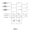
- Fig.5 is a timing chart for illustrating the operation of the solid-state image pickup device shown in Fig.2.
- the solid-state image pickup device includes a lens 1 for converging the image pickup light incident thereon, and a first birefringence plate 2, as a first electro-optical effect plate.
- An electrical field, applied across the birefringence plate 2 is turned on and off at a one-field interval, in such a manner that, when the voltage is turned off, the image pickup light radiated via lens 1 is directly radiated as an ordinary light without changing its optical path and, when the voltage is turned on, the image pickup light radiated via lens 1 is radiated as an ordinary light and an extraordinary light having an optical path shifted vertically upwards at a pitch equal to one-half pixel with respect to the optical path of the ordinary light.
- the image pickup device also includes a half wave plate or ⁇ /2 plate 3 for transforming the ordinary light radiated thereto when the voltage across the first birefringence plate 2 is turned off into an extraordinary light, and for radiating the resulting extraordinary light, while transforming the ordinary light and the extraordinary light radiated thereto when the voltage across the first birefringence plate 2 is turned on into the extraordinary light and the ordinary light, respectively, and for radiating the resulting extraordinary light and the ordinary light.
- the solid-state image pickup device also includes a second birefringence plate 4, as a second electro-optical effect plate.
- the electrical voltage applied across the birefringence plate 4 is turned on and off at a one-field interval at the same timing as that for the first birefringence plate 2, in such a manner that, when the voltage is turned off, the extraordinary light radiated via the first birefringence plate 2 and the ⁇ /2 plate 3 is directly transmitted without changing its optical path and, when the voltage is turned on, the optical path of the extraordinary light radiated via the first birefringence plate 2 and the ⁇ /2 plate 3 is shifted up to the optical path of the ordinary light, with the extraordinary light and the ordinary light being summed and transmitted.
- the solid-state image pickup device also includes a voltage-dependent transforming type color filter 5 which is driven with three different voltages for red (R), green (G) and blue (B), applied via a voltage terminal 8 as later described, and which is adapted for transforming the ordinary light and the extraordinary light, radiated via the second birefringence plate 4, into R, G or B image-pickup light rays, depending on the applied voltage values.
- the image pickup device includes a CCD image sensor 6, as a solid-state image pickup device, for receiving the color image-pickup light rays radiated thereto via color filter 5 to effect photoelectric transfer to generate and output the color image-pickup signals.
- the CCD image sensor may be a so-called interlaced scanning type device for reading out electrical charges from odd line pixels and even line pixels for an odd field and an even field, respectively.
- the CCD image sensor 6 is of the non-interlaced scanning type, that is, it is designed for reading electrical charges from the pixels of all of the lines of both the odd and even lines.
- each frame is completed by one field, in distinction from the device in which each frame is completed by an odd field and an even field. That is, there is no difference between the odd and even fields. Conversely, the odd and even fields simply mean two contiguous fields.
- the color filter 5 is constituted by a liquid crystal plate and, if a voltage V1 is applied thereto, it transmits only the image pickup light for red (R) of the radiated image pickup light. On the other hand, if a voltage V2 or V3 is applied thereto, it transmits only the radiated image pickup light for green (G) or the radiated image pick-up light for blue (B).
- the voltages V1, V2 and V3 are a.c. voltages which are increased sequentially in magnitude in this order, as shown in Fig.4. These a.c. voltages V1, V2 and V3 are changed over at a one-field interval, with the thus changed over a.c. voltages being applied across the color filter 5. Consequently, the three image-pickup light rays of R, G and B are radiated in this order at the one-field interval from the color filter 5.
- the ⁇ /2 plate 3 may for example be formed by a quartz plate.
- the plate 3 is formed by a twisted nematic phase liquid crystal plate. If the ⁇ /2 plate 3 is formed by a liquid crystal plate, it may be of an extremely small thickness as compared to the ⁇ /2 plate 3 formed by the quartz plate. Consequently, the first birefringence plate 2, ⁇ /2 plate 3, second birefringence plate 4 and the color filter 5 may be bonded to one another and easily affixed to the light receiving surface of the CCD image sensor 6.
- the solid-state image pickup device of the present invention is formed as a chip including various components excepting the lens 1, that is the first birefringence plate 2, ⁇ /2 plate 3, second birefringence plate 4, color filter 5 and the CCD image sensor 6.
- the image pickup light is converged by lens 1 and radiated to the first birefringence plate 2.
- the voltage applied across the first birefringence plate 2 is turned off and on, as shown at b in Fig.5, during an odd-field period corresponding to the time period between t1 and t4 and during an even-field period corresponding to the time period between t4 and t7, in timed relation to a field discrimination signal which goes low during the odd field period between time t1 and t4 and which goes high during the even field period between time t4 and t7, as shown at a in Fig.5.
- the first birefringence plate 2 radiates the image pickup light incident thereon as an ordinary light without changing its optical path.
- the first birefringence plate splits the image pickup light incident thereon into the above-mentioned ordinary light and an extraordinary light which has its optical path shifted vertically upwards by e.g. a pitch equal to one-half pixel with respect to the optical path of the ordinary light.
- the direction and magnitude of the shift of the optical path of the image pickup light by the first birefringence plate 2 and a second birefringence plate 4 as later explained may be adjusted in dependence upon the shape and/or the properties of the first and second birefringence plates 2, 4 and/or the direction of voltage application.
- the ordinary light and the extraordinary light, radiated from the first birefringence plate 2, are subsequently radiated on the ⁇ /2 plate 3.
- the ⁇ /2 plate 3 When irradiated with the ordinary light, the ⁇ /2 plate 3 radiates an extraordinary light transformed from the ordinary light with the optical path remaining unchanged. On the other hand, when irradiated with the extraordinary light, the ⁇ /2 plate 3 radiates an ordinary light converted from the extraordinary light with the optical path remaining unchanged.
- the ⁇ /2 plate 3 radiates the ordinary light as the extraordinary light during the odd field period.
- the ⁇ /2 plate 3 radiates the extraordinary light transformed from the ordinary light and the ordinary light transformed from the extraordinary light.
- An electrical voltage is applied across the second birefringence plate 4 at the same timing as that for the first birefringence plate 2, as shown at c in Fig.5. That is, the electrical voltage applied across the second birefringence plate 4 is turned off during the odd field period corresponding to a time interval between t1 and t4 and is turned on during the even field period corresponding to a time interval between t4 and t7, respectively.
- the second birefringence plate 4 directly radiates the extraordinary light without changing its optical path.
- the second birefringence plate 4 directly radiates the ordinary light without changing its optical path and, if irradiated with the extraordinary light during the voltage turn-on period, the second birefringence plate 4 shifts the optical path of the extraordinary light vertically upwards by a pitch equal to one-half pixel and radiates the thus shifted extraordinary light.
- the non-shifted image pickup light as the extraordinary light, which is radiated from the second birefringence plate 4 when the voltage applied thereto is turned off, may be made equal to the shifted image pickup light, which is the light equal to the sum of the extraordinary light and the ordinary light and which is radiated from the second birefringence plate 4 when the voltage supplied thereto is turned on.
- the ordinary light and the extraordinary light are summed together and radiated, instead of splitting the image pickup light radiated via lens 1 into the ordinary light and the extraordinary light and radiating a selected one of the ordinary light and the extraordinary light, for eliminating the loss in the light volume of the image pickup light before and after shifting.
- the ordinary light and the extraordinary light, radiated from the second birefringence plate 4, are radiated to the color filter 5.
- An electrical voltage having a voltage value of V1 is applied across the color filter 5 between time t1 and t2 during the odd field period and between time t4 and time t5 during the even field period, as shown at d in Fig.5.
- an electrical voltage having a voltage value of V2 is applied across the color filter 5 between time t2 and t3 during the odd field period and between time t5 and time t6 during the even field period, as shown at e in Fig.5
- an electrical voltage having a voltage value of V3 is applied across the color filter 5 between time t3 and t4 during the odd field period and between time t6 and time t7 during the even field period, as shown at f in Fig.5.
- the color filter 5 causes only the radiated image pickup light for red (R), for green (G) or for blue (B) to be transmitted therethrough when the voltage having the values of V1, V2 or V3 is applied thereto, respectively.
- the image pickup light which is the extraordinary light, radiated from the color filter 5 during a time interval between time t1 and t2 of the odd field period, is solely the image pickup light for red (R).
- the image pickup light, which is the extraordinary light, radiated from the color filter 5 during a time interval between time t2 and t3 of the odd field period is solely the image pickup light for green (G)
- the image pickup light, which is the extraordinary light, radiated from the color filter 5 during a time interval between time t3 and t4 of the odd field period is solely the image pickup light for blue (B).
- the image pickup light which is the ordinary light and the extraordinary light summed together, radiated during a time interval between time t4 and time t5 of the even field, is solely the image pickup light for red (R).
- the image pickup light which is the ordinary light and the extraordinary light summed together, radiated during a time interval between time t5 and time t6 of the even field, is solely the image pickup light for green (G)
- the image pickup light which is the ordinary light and the extraordinary light summed together, radiated during a time interval between time t6 and time t7 of the even field, is solely the image pickup light for blue (B).
- the CCD image sensor 6 receives the image pickup lights for various colors radiated thereto to effect photoelectric transfer to generate corresponding image pickup signals which are outputted. Since the image pickup light radiated on the CCD image sensor 6 is sequentially the image pickup light for red (R), image pickup light for green (G) and the image pickup light for blue (B), for each of the odd and even fields, as described above, the image pickup signals for red (R), for green (G) and for blue (B) are radiated from the CCD image sensor 6 in this order within each field.
- the image pickup signals from the CCD image sensor 6 are supplied via output terminals 7 to an image pickup signal processing circuit, not shown, where they are processed in predetermined manner, and subsequently transmitted to a monitor device etc. for display.
- the image pickup light for various colors, radiated on the CCD image sensor 6 via color filter 5 is also devoid of light volume losses.
- the image pickup signals for various colors having a satisfactory S/N ratio may be generated and outputted by the CD image sensor 6 to enable the dynamic range to be enlarged.
- the image pickup light radiated on the CCD image sensor 6 during the odd field period is the image pickup light, as the extraordinary light, for the various colors at the ordinary radiating positions
- the image pickup light radiated on the CCD image sensor 6 during the even field period is the image pickup light, as the ordinary light and the extraordinary light, summed together, for the various prime colors at the radiating positions shifted vertically upwardly from the usual radiating positions by a pitch equal to one-half pixel.
- the number of the horizontal scanning lines may be increased twofold thus improving the vertical resolution.
- the interlaced scanning type CCD image sensor is employed as the solid-state image pickup device, since the charge reading lines are different between the odd and the even fields, the resolution cannot be improved by radiating the image pickup light shifted for every other field vertically upwards at a one-half pixel pitch, unless a one-frame picture is formed by pictures of four or more fields. Besides, if a one-frame picture is formed by four or more fields, the resolution cannot be improved significantly if the picture to be imaged is a moving picture.
- the image pickup device includes a non-interlaced scanning type solid-state image pickup device, (the above-mentioned CCD image sensor 6) as the solid-state image pickup device.
- the non-interlaced scanning type CCD image sensor reads out signal charges from the pixels of the totality of the lines both during the scanning of the odd fields and the scanning of the even fields, similarly to the above-mentioned interlaced scanning type CCD image sensor.
- the image pickup signals for an odd field and those for an even field are outputted for the first field and for the second field, respectively, so that the image pickup signals similar to those produced by interlaced scanning may be outputted despite the fact that the non-interlaced scanning type CCD image is employed, so that a picture of a high resolution may be produced with two fields.
- the resolution may be improved even although the picture to be imaged is a moving picture.
- the essential components except the lens 1, that is the above-mentioned first birefringence plate 2, ⁇ /2 plate 3, which is a twisted nematic phase liquid crystal plate, second birefringence plate 4, color filter 5 and the CCD image sensor 6, are formed in one chip.
- the result is reduction in a mounting floor space for the solid-state image pickup device, contributing to reduction in size of the equipment such as the video camera unit in which the solid-state image pickup device is to be mounted.
- the ⁇ /2 plate 3 is fabricated from an inexpensive liquid crystal plate. Consequently, the solid-state image pickup device may be fabricated at low costs to contribute to cost reduction of the equipment, such as the video camera unit.
- the basic concept of the present invention resides in that there are provided, at a pre-stage of the CCD image sensor, a first birefringence plate directly radiating the image pickup light as the ordinary light, when the voltage is turned off, with the optical path of the image pickup light remaining unchanged, and radiating the ordinary light and an extraordinary light having its optical path shifted by a predetermined amount with respect to the optical path of the ordinary light, when the voltage is turned off, a ⁇ /2 plate for transforming the ordinary light radiated thereto into an extraordinary light and radiating the resulting extraordinary light and for radiating the extraordinary light radiated thereto as the ordinary light, and a second birefringence plate for directly radiating the extraordinary light radiated thereto when the voltage is turned off and for directly radiating the extraordinary light when the voltage is turned on, with the optical path remaining unchanged and radiating the ordinary light with a optical path shift of a predetermined amount in this sequence, and in that the voltage supplied across the first and second birefringence plates are turned on and off simultaneously to prevent light volume losses
- the present invention is not limited to the above-described particular constitution.
- color filters for R, G and B colors may be provided on the pixels of the CCD image sensor, instead of providing the color filter 5.
- the CCD image sensor may be of the monochromatic type.
- the ⁇ /2 plate 3 may be formed of a quartz plate, while the CCD image sensor of the interlaced scanning type may also be employed.
- the basic concept of the present invention also consists in fabricating the ⁇ /2 plate 3 from a liquid crystal plate and mounting it on the CCD image sensor along with the second birefringence plate for providing the solid-state image pickup device by one chip.
- the color filters for R, G and B colors may be provided on the pixels of the CCD image sensor, instead of providing the color filter 5, as mentioned above.
- the CCD image sensor may be of the monochromatic type.
- the CCD image sensor for interlaced scanning may also be used as the CCD image sensor.
Description
- This invention relates to a solid-state image pickup device in accordance with the precharacterizing part of
claim 1. Such a solid-state image pickup device is known from US-A-5 091 795. - A solid-state image pickup device, or a CCD image sensor, is extensively used in video cameras or image scanners because of its small size and low power consumption. The CCD image sensor, having a number of pixels on the order of 400 000, is usually mounted on the video camera. However, the CCD image sensor, having the number of the pixels on the order of 400 000, is inferior in resolution to an image tube. Recently, a high resolution television receiver, known as a high-definition (HD) television receiver, has become popular, and a CD image sensor having the number of the pixels increased to 2 000 000 has been developed by reducing the pixel area in order to cope with the HD television receiver. However, if the pixel area is reduced, output image pickup signals of the solid-state image pickup device is lowered in signal level to deteriorate the S/N ratio. In view of the lowering of the S/N ratio, the number of 2,000,00 pixels of the solid-state image pickup device represents a possible upper limit such that it has become difficult to increase the number of pixels to improve the resolution further. On the other hand, since the CCD image sensor having 2,000,000 pixels is insufficient in resolution if it is to be used for inputting a printed text, a demand for for a higher resolution has been raised.
- For coping with the above problem, a solid-state image pickup device has been developed, in which the relative position between the solid-state image-pickup device (CCD image sensor) and the image pickup light is shifted in an amount equal to one or more integer fractions of the pixel pitch during imaging for increasing resolution by increasing the spatial sampling area without increasing the number of pixels.
- With such solid-state image pickup device, the CCD image sensor is mounted on a piezoelectric element and oscillated in one direction from field to field at an amplitude equal to a half pixel pitch for shifting the image pickup light radiated on the CCD image sensor by a pitch equal to a half pixel by way of image shifting for increasing the spatial sampling area for achieving a picture of high resolution without increasing the number of pixels.
- There has also been known a solid-state image pickup device in which a thin glass plate is mounted on the front face of the CCD image sensor and oscillated at an extreme small angle during imaging. With such solid-state image pickup device, the image pickup light radiated on the CCC image sensor is image-shifted each time the glass plate is oscillated for increasing the spatial sampling area for achieving a picture of high resolution without increasing the number of pixels.
- However, with such solid-state image pickup devices, since the image pickup light radiated or the CCD image sensor is image-shifted by mechanical vibrations applied to the CCD image sensor itself or to the glass plate mounted ahead of the CCD image sensor, not only the mechanical structure becomes more complex but also the reliability of image shifting is rather low.
- To avoid the defect inherent in the solid-state image pickup device which carries out the image shifting by mechanical means, there has also been developed a solid-state image pickup device in which image shifting may be realized by electrical means.
- The solid-state image pickup device with electrical image shifting is arranged as shown for example in Fig.1. When the image pickup is started with the sclid-state image pickup device, the image pickup light is converged by a
lens 50 so as to be radiated on abirefringence plate 51. - When irradiated with the image pickup light from
lens 50, thebirefringence plate 51 splits the light into an ordinary light and an extraordinary light having an optical path shifted from the optical path of the ordinary light vertically upwards by a pitch equal to one-half pixel so as to cause these light rays to be radiated on a voltage-controlled opticalpath selecting plate 52. - The voltage-controlled optical
path selecting pate 52 is made up e.g. of a liquid crystal plate and a polarization plate. An electrical voltage is applied to the liquid crystal plate at a one-field interval. When the electrical voltage is not applied to the liquid crystal plate, the ordinary light and the extraordinary light, radiated to the liquid crystal plate via thebirefringence plate 51, are directly transmitted through the liquid crystal plate and only the ordinary light is transmitted through the polarization plate. When the electrical voltage is applied to the liquid crystal plate, the ordinary light and the extraordinary light, radiated to the liquid crystal plate via thebirefringence plate 51, are polarized by 90° when passed through the liquid crystal plate, with the respective optical paths remaining unchanged. Of these light rays, solely the extraordinary light is transmitted through the polarization plate. In this manner, the ordinary light or the extraordinary light is selectively radiated from the voltage-controlled opticalpath selecting plate 52, at a one-field interval, so as to be radiated on aCCD image sensor 53. - The
CCD image sensor 53 receives the ordinary light and extraordinary light to effect photoelectric transfer to generate image-pickup signals which are outputted at anoutput terminal 54. It is noted that not only the ordinary light but also the extraordinary light having an optical path shifted vertically upwards by a pitch equal to one-half pixel with respect to the optical path of the ordinary light is radiated on theCCD image sensor 53. - This leads to an increased spatial sampling area and to increased resolution.
- As compared to a solid-state image pickup device, effecting the image shifting by mechanical means, the solid-state image pickup device, effecting the electrical image shifting, avoids moving parts of a complicated mechanical system, and hence achieves improved reliability in the image shifting and a simplified structure of the device in its entirety.
- However, with the above-described solid-state image pickup device, the image pickup light is split by the
birefringence plate 51 into the ordinary light and the extraordinary light and the electrical voltage applied across theselecting plate 52 is on/off controlled for selecting one of the ordinary light and the extraordinary light from thebirefringence plate 51 for radiating the selected light to theCCD image sensor 53. Consequently, the intensity of the image pickup light radiated on theCCD image sensor 53 is reduced to substantially one-half of the original image pickup light intensity so that only a dark image may be produced. - On the other hand, the recent tendency is towards an increasingly small size of a video camera unit etc. and a demand has been raised for the electrically image-shifting type solid-state image pickup device fabricated in one chip.
- The solid-state image pickup device known from US-A-5 091 795 which corresponds to the precharacterizing part of claim has as its primary object to provide an optical-lowpass filter which can be favourably used for solid-state image sensors and which can remove the Moiré, is not low in the resolving power and be made thin in the thickness. To achieve this object the known device includes an arrangement of two lowpass filters overlapped with each other and 1/2-wave plate arranged between them to remove the Moire by shaking and obscuring the image. For that purpose a AC-driving voltage is synchronously applied to the two lowpass filters which are in the embodiment of fig. 12 of US-A-5 091 795 liquid crystal devices, respectively. The exit position of the exit light will result in oscillation with a certain amplitude by changing the amplitude of the AC-driving voltage applied to the two liquid crystal devices at a speed higher than a predetermined value, e.g. at a speed higher than twice the read-out period of a charged coupled device. The displacement or certain amplitude will vary continuously and periodically or at random when the wave shape of the voltage to be applied is varied.
- It is therefore an object of the present invention to provide a solid-state image pickup device which achieves an excellent resolution and avoids loss of light intensity to assure a lighter image and may be fabricated in one chip to contribute to reduction in size of the equipment such as a video camera unit.
- The above object is achieved by a solid-state image pickup device comprising first electro-optical effect means selectively operable in a first mode or a second mode, said first electro-optical effect means being designed for splitting an incident image pickup light into an ordinary light ray and an extraordinary light ray having its optical axis shifted vertically with respect to that of said ordinary light ray for said first mode and for transmitting said incident image pickup light as an ordinary light ray for said second mode, light transforming means for transforming said ordinary light ray from said first electro-optical effect means into an extraordinary light ray and for transforming said extraordinary light ray from said first electro-optical effect means into an ordinary light ray, second electro-optical effect means selectively operable in a first mode or a second mode, said second electro-optical effect means being designed to transmit said ordinary light ray from said light transforming means and to shift the optical axis of said extraordinary light ray vertically with respect to that of said ordinary light ray so that said extraordinary light ray and said ordinary light ray are mixed together for said first mode, said second electro-optical effect means being designed to transmit said extraordinary light ray from said light transforming means for said second mode, and image sensor means for transforming said ordinary light ray and said extraordinary light ray from said second electro-optical effect means (4) into electrical signals,
characterized in
that switching means are provided to selectively switch said first and second electro-optical effect means to select said first mode and said second mode periodical at a one-field interval, and said extraordinary light ray is shifted by a pitch equal to one-half pixel by said first and second electro-optical means for said first mode, wherein said image sensor means are operated by non-interlaced scanning. - With the solid-state image pickup device according to the present invention, the light transforming means is formed by a liquid crystal plate and is provided on the solid-state image sensor along with the first and second electro-optical effect plates to enable the entire device to be formed in one chip.
- When the image pickup operation by the solid-state image pickup operation is initiated, an electrical voltage is applied at e.g. every one-half field to the first electro-optical effect plate. When the voltage is turned off, the first electro-optical effect plate directly radiates the image pickup light radiated thereto as an ordinary light without changing its optical path.
- Conversely, when the voltage is turned on, the first electro-optical plate radiates the image pickup light in the form of an ordinary light and an extraordinary light having its optical axis shifted a predetermined amount with respect to the optical axis of the ordinary light. The ordinary light and the extraordinary light are radiated on the light transforming means.
- The second electro-optical effect plate has an electrical voltage applied thereto turned on and off at the same timing as the first electro-optical effect plate, so that, when the voltage is turned off, it directly radiates the extraordinary light radiated thereto via the first electro-optical effect plate and the light transforming means without changing its optical path. When the voltage is turned off, the second electro-optical effect plate shifts the optical path of the extraordinary light radiated thereto via the first electro-optical effect plate and the light transforming means up to the optical path of the ordinary light. The extraordinary light is summed to the ordinary light and the combined light is radiated from the second electro-optical effect plate.
- Consequently, if the voltage applied across the first and second electro-optical effect plates is turned off, the image pickup light is not split into the ordinary light and the extraordinary light, so that the image pickup light is radiated on the solid-state image pickup device as the extraordinary light without its optical path being changed. If the voltage applied across the first and second electro-optical effect plates is turned on, the image pickup light is split by the first electro-optical effect plate into the ordinary light and the shifted extraordinary light which is transformed by light transforming means into the ordinary light which is radiated on the second electro-optical effect plate. The ordinary light is transformed by the light transforming means into an extraordinary light which is radiated on the second electro-optical effect plate. When the electrical voltage is applied across the electro-optical effect plates, the extraordinary light has its optical path shifted as described above, and is combined with the ordinary light transformed by the light transforming means into the extraordinary light so as to be radiated on the image pickup device.
- The result is image shifting devoid of light volume losses. Besides, the solid-state image pickup device according to the present invention may be formed in one chip by fabricating the light transforming means by a liquid crystal plate and by mounting the liquid crystal plate on the solid-state image pickup device along with the first and second electro-optical effect plates.
- The result is the reduced mounting area for the solid-state image pickup device.
- Other objects and advantages of the present invention will become more apparent from the following description of the preferred embodiments and the claims.
- Fig.1 is a block diagram showing a conventional image pickup device.
- Fig.2 is a block diagram showing an embodiment of a solid-state image pickup device according to the present invention.
- Fig.3 is a graph showing the relation between the a.c. voltage applied across a color filter provided in the solid-state image pickup device shown in Fig.2 and light components transmitted through the color filter.
- Fig.4 is a graph for illustrating the a.c. voltage applied across the color filter.
- Fig.5 is a timing chart for illustrating the operation of the solid-state image pickup device shown in Fig.2.
- Referring to Fig.2, the solid-state image pickup device according to the present invention includes a
lens 1 for converging the image pickup light incident thereon, and afirst birefringence plate 2, as a first electro-optical effect plate. An electrical field, applied across thebirefringence plate 2, is turned on and off at a one-field interval, in such a manner that, when the voltage is turned off, the image pickup light radiated vialens 1 is directly radiated as an ordinary light without changing its optical path and, when the voltage is turned on, the image pickup light radiated vialens 1 is radiated as an ordinary light and an extraordinary light having an optical path shifted vertically upwards at a pitch equal to one-half pixel with respect to the optical path of the ordinary light. The image pickup device also includes a half wave plate or λ/2plate 3 for transforming the ordinary light radiated thereto when the voltage across thefirst birefringence plate 2 is turned off into an extraordinary light, and for radiating the resulting extraordinary light, while transforming the ordinary light and the extraordinary light radiated thereto when the voltage across thefirst birefringence plate 2 is turned on into the extraordinary light and the ordinary light, respectively, and for radiating the resulting extraordinary light and the ordinary light. - The solid-state image pickup device also includes a
second birefringence plate 4, as a second electro-optical effect plate. The electrical voltage applied across thebirefringence plate 4 is turned on and off at a one-field interval at the same timing as that for thefirst birefringence plate 2, in such a manner that, when the voltage is turned off, the extraordinary light radiated via thefirst birefringence plate 2 and the λ/2plate 3 is directly transmitted without changing its optical path and, when the voltage is turned on, the optical path of the extraordinary light radiated via thefirst birefringence plate 2 and the λ/2plate 3 is shifted up to the optical path of the ordinary light, with the extraordinary light and the ordinary light being summed and transmitted. The solid-state image pickup device also includes a voltage-dependent transformingtype color filter 5 which is driven with three different voltages for red (R), green (G) and blue (B), applied via avoltage terminal 8 as later described, and which is adapted for transforming the ordinary light and the extraordinary light, radiated via thesecond birefringence plate 4, into R, G or B image-pickup light rays, depending on the applied voltage values. Finally, the image pickup device includes aCCD image sensor 6, as a solid-state image pickup device, for receiving the color image-pickup light rays radiated thereto viacolor filter 5 to effect photoelectric transfer to generate and output the color image-pickup signals. - The CCD image sensor may be a so-called interlaced scanning type device for reading out electrical charges from odd line pixels and even line pixels for an odd field and an even field, respectively. However, with the present embodiment, the
CCD image sensor 6 is of the non-interlaced scanning type, that is, it is designed for reading electrical charges from the pixels of all of the lines of both the odd and even lines. - With the non-interlaced scanning type device, each frame is completed by one field, in distinction from the device in which each frame is completed by an odd field and an even field. That is, there is no difference between the odd and even fields. Conversely, the odd and even fields simply mean two contiguous fields.
- The
color filter 5 is constituted by a liquid crystal plate and, if a voltage V1 is applied thereto, it transmits only the image pickup light for red (R) of the radiated image pickup light. On the other hand, if a voltage V2 or V3 is applied thereto, it transmits only the radiated image pickup light for green (G) or the radiated image pick-up light for blue (B). The voltages V1, V2 and V3 are a.c. voltages which are increased sequentially in magnitude in this order, as shown in Fig.4. These a.c. voltages V1, V2 and V3 are changed over at a one-field interval, with the thus changed over a.c. voltages being applied across thecolor filter 5. Consequently, the three image-pickup light rays of R, G and B are radiated in this order at the one-field interval from thecolor filter 5. - The λ/2
plate 3 may for example be formed by a quartz plate. In the present case, theplate 3 is formed by a twisted nematic phase liquid crystal plate. If the λ/2plate 3 is formed by a liquid crystal plate, it may be of an extremely small thickness as compared to the λ/2plate 3 formed by the quartz plate. Consequently, thefirst birefringence plate 2, λ/2plate 3,second birefringence plate 4 and thecolor filter 5 may be bonded to one another and easily affixed to the light receiving surface of theCCD image sensor 6. Thus the solid-state image pickup device of the present invention is formed as a chip including various components excepting thelens 1, that is thefirst birefringence plate 2, λ/2plate 3,second birefringence plate 4,color filter 5 and theCCD image sensor 6. - The operation of the above-described solid-state image pickup device according to the present invention is hereinafter explained.
- Referring to Fig.2, when the image pickup operation of the solid-state image pickup device according to the present invention is initiated, the image pickup light is converged by
lens 1 and radiated to thefirst birefringence plate 2. - The voltage applied across the
first birefringence plate 2 is turned off and on, as shown at b in Fig.5, during an odd-field period corresponding to the time period between t1 and t4 and during an even-field period corresponding to the time period between t4 and t7, in timed relation to a field discrimination signal which goes low during the odd field period between time t1 and t4 and which goes high during the even field period between time t4 and t7, as shown at a in Fig.5. - When the voltage is turned off, the
first birefringence plate 2 radiates the image pickup light incident thereon as an ordinary light without changing its optical path. However, when the voltage is turned on, the first birefringence plate splits the image pickup light incident thereon into the above-mentioned ordinary light and an extraordinary light which has its optical path shifted vertically upwards by e.g. a pitch equal to one-half pixel with respect to the optical path of the ordinary light. - Consequently, only the ordinary light is radiated from the
first birefringence plate 2 during the odd field period, whereas the ordinary light and the extraordinary light, split from the image pickup light and radiated from thefirst birefringence plate 2 during the even field period. - Meanwhile, the direction and magnitude of the shift of the optical path of the image pickup light by the
first birefringence plate 2 and asecond birefringence plate 4 as later explained may be adjusted in dependence upon the shape and/or the properties of the first andsecond birefringence plates - The ordinary light and the extraordinary light, radiated from the
first birefringence plate 2, are subsequently radiated on the λ/2plate 3. - When irradiated with the ordinary light, the λ/2
plate 3 radiates an extraordinary light transformed from the ordinary light with the optical path remaining unchanged. On the other hand, when irradiated with the extraordinary light, the λ/2plate 3 radiates an ordinary light converted from the extraordinary light with the optical path remaining unchanged. - Thus the λ/2
plate 3 radiates the ordinary light as the extraordinary light during the odd field period. During the even field period, on the other hand, the λ/2plate 3 radiates the extraordinary light transformed from the ordinary light and the ordinary light transformed from the extraordinary light. - The ordinary light and the extraordinary light, radiated from the λ/2
plate 3, are radiated on thesecond birefringence plate 4. - An electrical voltage is applied across the
second birefringence plate 4 at the same timing as that for thefirst birefringence plate 2, as shown at c in Fig.5. That is, the electrical voltage applied across thesecond birefringence plate 4 is turned off during the odd field period corresponding to a time interval between t1 and t4 and is turned on during the even field period corresponding to a time interval between t4 and t7, respectively. - If irradiated with the extraordinary light during the voltage turn-off period, the
second birefringence plate 4 directly radiates the extraordinary light without changing its optical path. On the other hand, if irradiated with the ordinary light during the voltage turn-on period, thesecond birefringence plate 4 directly radiates the ordinary light without changing its optical path and, if irradiated with the extraordinary light during the voltage turn-on period, thesecond birefringence plate 4 shifts the optical path of the extraordinary light vertically upwards by a pitch equal to one-half pixel and radiates the thus shifted extraordinary light. - Consequently, during the odd field period, when the voltage is turned off, the extraordinary light from the λ/2
plate 3 is directly radiated from thesecond birefringence plate 4, without its optical path being changed. On the other hand, during the even field period, when the voltage is turned on, the extraordinary light incident on the λ/2plate 3 is directly radiated, without its optical path being changed, while the ordinary light incident on the λ/2plate 3 has its optical path shifted vertically upwards by a pitch equal to one-half pixel. And the thus shifted ordinary light is radiated. Consequently, when the voltage across thesecond birefringence plate 4 is turned on, the ordinary light and the extraordinary light are summed together and outputted from theplate 4. The non-shifted image pickup light, as the extraordinary light, which is radiated from thesecond birefringence plate 4 when the voltage applied thereto is turned off, may be made equal to the shifted image pickup light, which is the light equal to the sum of the extraordinary light and the ordinary light and which is radiated from thesecond birefringence plate 4 when the voltage supplied thereto is turned on. - Besides, while the image pickup light irradiated via
lens 1 is split into the ordinary light and the extraordinary light for optical axis shifting, the ordinary light and the extraordinary light are summed together and radiated, instead of splitting the image pickup light radiated vialens 1 into the ordinary light and the extraordinary light and radiating a selected one of the ordinary light and the extraordinary light, for eliminating the loss in the light volume of the image pickup light before and after shifting. - The ordinary light and the extraordinary light, radiated from the
second birefringence plate 4, are radiated to thecolor filter 5. - An electrical voltage having a voltage value of V1 is applied across the
color filter 5 between time t1 and t2 during the odd field period and between time t4 and time t5 during the even field period, as shown at d in Fig.5. Similarly, an electrical voltage having a voltage value of V2 is applied across thecolor filter 5 between time t2 and t3 during the odd field period and between time t5 and time t6 during the even field period, as shown at e in Fig.5, and an electrical voltage having a voltage value of V3 is applied across thecolor filter 5 between time t3 and t4 during the odd field period and between time t6 and time t7 during the even field period, as shown at f in Fig.5. - The
color filter 5 causes only the radiated image pickup light for red (R), for green (G) or for blue (B) to be transmitted therethrough when the voltage having the values of V1, V2 or V3 is applied thereto, respectively. - Consequently, the image pickup light, which is the extraordinary light, radiated from the
color filter 5 during a time interval between time t1 and t2 of the odd field period, is solely the image pickup light for red (R). Similarly, the image pickup light, which is the extraordinary light, radiated from thecolor filter 5 during a time interval between time t2 and t3 of the odd field period, is solely the image pickup light for green (G), whereas the image pickup light, which is the extraordinary light, radiated from thecolor filter 5 during a time interval between time t3 and t4 of the odd field period, is solely the image pickup light for blue (B). - On the other hand, the image pickup light, which is the ordinary light and the extraordinary light summed together, radiated during a time interval between time t4 and time t5 of the even field, is solely the image pickup light for red (R). Similarly, the image pickup light, which is the ordinary light and the extraordinary light summed together, radiated during a time interval between time t5 and time t6 of the even field, is solely the image pickup light for green (G), whereas the image pickup light, which is the ordinary light and the extraordinary light summed together, radiated during a time interval between time t6 and time t7 of the even field, is solely the image pickup light for blue (B).
- The image pickup light rays for various colors, radiated from the
color filter 5, are radiated to theCCD image sensor 6. - The
CCD image sensor 6 receives the image pickup lights for various colors radiated thereto to effect photoelectric transfer to generate corresponding image pickup signals which are outputted. Since the image pickup light radiated on theCCD image sensor 6 is sequentially the image pickup light for red (R), image pickup light for green (G) and the image pickup light for blue (B), for each of the odd and even fields, as described above, the image pickup signals for red (R), for green (G) and for blue (B) are radiated from theCCD image sensor 6 in this order within each field. - The result is that, by using a one-chip CCD image sensor, it becomes possible to output RGB component signals as in the case of a solid-state image pickup device employing separate CCD image sensors for red (R), green (G) and blue (B), that is a so-called three CCD type solid-state image pickup device.
- The image pickup signals from the
CCD image sensor 6 are supplied viaoutput terminals 7 to an image pickup signal processing circuit, not shown, where they are processed in predetermined manner, and subsequently transmitted to a monitor device etc. for display. - Since the non-shifted image pickup light free of light volume losses and the shifted image pickup light are radiated to the
color filter 5, the image pickup light for various colors, radiated on theCCD image sensor 6 viacolor filter 5, is also devoid of light volume losses. - Consequently, the image pickup signals for various colors having a satisfactory S/N ratio may be generated and outputted by the
CD image sensor 6 to enable the dynamic range to be enlarged. - Besides, the image pickup light radiated on the
CCD image sensor 6 during the odd field period is the image pickup light, as the extraordinary light, for the various colors at the ordinary radiating positions, whereas the image pickup light radiated on theCCD image sensor 6 during the even field period is the image pickup light, as the ordinary light and the extraordinary light, summed together, for the various prime colors at the radiating positions shifted vertically upwardly from the usual radiating positions by a pitch equal to one-half pixel. In this manner, the number of the horizontal scanning lines may be increased twofold thus improving the vertical resolution. - It is noted that, if the interlaced scanning type CCD image sensor is employed as the solid-state image pickup device, since the charge reading lines are different between the odd and the even fields, the resolution cannot be improved by radiating the image pickup light shifted for every other field vertically upwards at a one-half pixel pitch, unless a one-frame picture is formed by pictures of four or more fields. Besides, if a one-frame picture is formed by four or more fields, the resolution cannot be improved significantly if the picture to be imaged is a moving picture.
- However, the image pickup device according to the present invention includes a non-interlaced scanning type solid-state image pickup device, (the above-mentioned CCD image sensor 6) as the solid-state image pickup device. The non-interlaced scanning type CCD image sensor reads out signal charges from the pixels of the totality of the lines both during the scanning of the odd fields and the scanning of the even fields, similarly to the above-mentioned interlaced scanning type CCD image sensor. Consequently, when the above-mentioned image pickup light, which is vertically upwardly shifted at a pitch equal to one-half pixel for every other field, is radiated on the CCD image sensor, the image pickup signals for an odd field and those for an even field are outputted for the first field and for the second field, respectively, so that the image pickup signals similar to those produced by interlaced scanning may be outputted despite the fact that the non-interlaced scanning type CCD image is employed, so that a picture of a high resolution may be produced with two fields.
- Besides, since the picture of high resolution may be produced with two fields, the resolution may be improved even although the picture to be imaged is a moving picture.
- In addition, with the solid-state image pickup device according to the present invention, the essential components except the
lens 1, that is the above-mentionedfirst birefringence plate 2, λ/2plate 3, which is a twisted nematic phase liquid crystal plate,second birefringence plate 4,color filter 5 and theCCD image sensor 6, are formed in one chip. - The result is reduction in a mounting floor space for the solid-state image pickup device, contributing to reduction in size of the equipment such as the video camera unit in which the solid-state image pickup device is to be mounted.
- On the other hand, the λ/2
plate 3 is fabricated from an inexpensive liquid crystal plate. Consequently, the solid-state image pickup device may be fabricated at low costs to contribute to cost reduction of the equipment, such as the video camera unit. - Finally, the basic concept of the present invention resides in that there are provided, at a pre-stage of the CCD image sensor, a first birefringence plate directly radiating the image pickup light as the ordinary light, when the voltage is turned off, with the optical path of the image pickup light remaining unchanged, and radiating the ordinary light and an extraordinary light having its optical path shifted by a predetermined amount with respect to the optical path of the ordinary light, when the voltage is turned off, a λ/2 plate for transforming the ordinary light radiated thereto into an extraordinary light and radiating the resulting extraordinary light and for radiating the extraordinary light radiated thereto as the ordinary light, and a second birefringence plate for directly radiating the extraordinary light radiated thereto when the voltage is turned off and for directly radiating the extraordinary light when the voltage is turned on, with the optical path remaining unchanged and radiating the ordinary light with a optical path shift of a predetermined amount in this sequence, and in that the voltage supplied across the first and second birefringence plates are turned on and off simultaneously to prevent light volume losses of the non-shifted image pickup light and the shifted image pickup light which are to be radiated on the CCD image sensor. Consequently, the present invention is not limited to the above-described particular constitution. For example, color filters for R, G and B colors may be provided on the pixels of the CCD image sensor, instead of providing the
color filter 5. The CCD image sensor may be of the monochromatic type. Besides, the λ/2plate 3 may be formed of a quartz plate, while the CCD image sensor of the interlaced scanning type may also be employed. - The basic concept of the present invention also consists in fabricating the λ/2
plate 3 from a liquid crystal plate and mounting it on the CCD image sensor along with the second birefringence plate for providing the solid-state image pickup device by one chip. In such case, It is difficult to fabricate the λ/2plate 3 from a quartz plate to provide the one-chip device. However, the color filters for R, G and B colors may be provided on the pixels of the CCD image sensor, instead of providing thecolor filter 5, as mentioned above. alternatively, the CCD image sensor may be of the monochromatic type. Besides, the CCD image sensor for interlaced scanning may also be used as the CCD image sensor.
Claims (6)
- A solid-state image pickup device comprising first electro-optical effect means (2) selectively operable in a first mode or a second mode, said first electro-optical effect means (2) being designed for splitting an incident image pickup light into an ordinary light ray and an extraordinary light ray having its optical axis shifted vertically with respect to that of said ordinary light ray for said first mode and for transmitting said incident image pickup light as an ordinary light ray for said second mode, light transforming means (3) for transforming said ordinary light ray from said first electro-optical effect means (2) into an extraordinary light ray and for transforming said extraordinary light ray from said first electro-optical effect means (2) into an ordinary light ray, second electro-optical effect means (4) selectively operable in a first mode or a second mode, said second electro-optical effect means being designed to transmit said ordinary light ray from said light transforming means (3) and to shift the optical axis of said extraordinary light ray vertically with respect to that of said ordinary light ray so that said extraordinary light ray and said ordinary light ray are mixed together for said first mode, said second electro-optical effect means (4) being designed to transmit said extraordinary light ray from said light transforming means (3) for said second mode, and image sensor means (6) for transforming said ordinary light ray and said extraordinary light ray from said second electro-optical effect means (4) into electrical signals,
characterized in
that switching means are provided to selectively switch said first and second electro-optical effect means (2, 4) to select said first mode and said second mode periodical at a one-field interval, and said extraordinary light ray is shifted by a pitch equal to one-half pixel by said first and second electro-optical means for said first mode, wherein said image sensor means (6) are operated by non-interlaced scanning. - The image pickup device as claimed in claim 1 wherein said first electro-optical effect means is controlled by an electric signal for selecting one of said first and second modes.
- The image pickup device as claimed in claim 1 wherein said first electro-optical effect means is a low-pass filter.
- The image pickup device as claimed in claim 1 wherein said light transforming means is a half wave plate.
- The image pickup device as claimed in claim 1 wherein said image sensor means is a charge-coupled device.
- The image pickup device as claimed in claim 1 wherein said first electro-optical means, light converging means and the second electro-optical means are formed on said image sensor means.
Applications Claiming Priority (2)
| Application Number | Priority Date | Filing Date | Title |
|---|---|---|---|
| JP152130/92 | 1992-06-11 | ||
| JP15213092A JP3380913B2 (en) | 1992-06-11 | 1992-06-11 | Solid-state imaging device |
Publications (2)
| Publication Number | Publication Date |
|---|---|
| EP0573997A1 EP0573997A1 (en) | 1993-12-15 |
| EP0573997B1 true EP0573997B1 (en) | 1997-10-01 |
Family
ID=15533716
Family Applications (1)
| Application Number | Title | Priority Date | Filing Date |
|---|---|---|---|
| EP93109316A Expired - Lifetime EP0573997B1 (en) | 1992-06-11 | 1993-06-09 | Solid-state image pick-up device with optical path shifting |
Country Status (4)
| Country | Link |
|---|---|
| US (1) | US5369266A (en) |
| EP (1) | EP0573997B1 (en) |
| JP (1) | JP3380913B2 (en) |
| DE (1) | DE69314230T2 (en) |
Families Citing this family (50)
| Publication number | Priority date | Publication date | Assignee | Title |
|---|---|---|---|---|
| US5659411A (en) * | 1993-06-18 | 1997-08-19 | Sony Corporation | Optical device having an optically transparent birefringent medium that selectively shifts the optical axis |
| JPH0794691A (en) * | 1993-09-21 | 1995-04-07 | Nikon Corp | Image sensor |
| US6243055B1 (en) | 1994-10-25 | 2001-06-05 | James L. Fergason | Optical display system and method with optical shifting of pixel position including conversion of pixel layout to form delta to stripe pattern by time base multiplexing |
| US5572341A (en) * | 1994-10-25 | 1996-11-05 | Fergason; James L. | Electro-optical dithering system using birefringence for optical displays and method |
| US5715029A (en) * | 1994-10-25 | 1998-02-03 | Fergason; James L. | Optical dithering system using birefringence for optical displays and method |
| US5537256A (en) * | 1994-10-25 | 1996-07-16 | Fergason; James L. | Electronic dithering system using birefrigence for optical displays and method |
| US6184969B1 (en) * | 1994-10-25 | 2001-02-06 | James L. Fergason | Optical display system and method, active and passive dithering using birefringence, color image superpositioning and display enhancement |
| US6061103A (en) * | 1995-01-20 | 2000-05-09 | Olympus Optical Co., Ltd. | Image display apparatus |
| US5585622A (en) * | 1995-03-23 | 1996-12-17 | Northrop Grumman Corporation | Optical sensor with mirror toggling |
| US6005682A (en) * | 1995-06-07 | 1999-12-21 | Xerox Corporation | Resolution enhancement by multiple scanning with a low-resolution, two-dimensional sensor array |
| US5834761A (en) * | 1996-03-22 | 1998-11-10 | Sharp Kabushiki Kaisah | Image input apparatus having a spatial filter controller |
| JP3617887B2 (en) * | 1996-10-14 | 2005-02-09 | シャープ株式会社 | Imaging device |
| US6567189B1 (en) | 1998-01-23 | 2003-05-20 | Canon Kabushiki Kaisha | Image reading apparatus |
| US6560382B1 (en) * | 1999-02-18 | 2003-05-06 | The United States Of America As Represented By The Secretary Of The Navy | System for alternately directing optical energy through multiple optical modulation channels |
| US6505037B1 (en) * | 1999-06-29 | 2003-01-07 | Sharp Laboratories Of America, Inc. | Data unit detection including antenna diversity |
| US7116370B1 (en) | 2000-03-31 | 2006-10-03 | Sharp Laboratories Of Ameria, Inc. | Image processing system optical shifting mechanism |
| JP2002268014A (en) * | 2001-03-13 | 2002-09-18 | Olympus Optical Co Ltd | Image display device |
| US6750438B2 (en) * | 2001-03-14 | 2004-06-15 | The United States Of America As Represented By The Administrator Of The National Aeronautics And Space Administration | Single-element electron-transfer optical detector system |
| US7064740B2 (en) | 2001-11-09 | 2006-06-20 | Sharp Laboratories Of America, Inc. | Backlit display with improved dynamic range |
| US7304705B2 (en) | 2002-03-26 | 2007-12-04 | Ricoh Company, Ltd. | Imaging unit, optical write unit, optical read unit and image forming apparatus |
| US8243004B2 (en) | 2003-03-10 | 2012-08-14 | Fergason Patent Properties, Llc | Apparatus and method for preparing, storing, transmitting and displaying images |
| US7083283B2 (en) * | 2003-07-22 | 2006-08-01 | Seiko Epson Corporation | Projector |
| US7021766B2 (en) * | 2003-07-22 | 2006-04-04 | Seiko Epson Corporation | Projector |
| WO2005052673A2 (en) | 2003-11-21 | 2005-06-09 | Sharp Laboratories Of America, Inc. | Liquid crystal display with adaptive color |
| US7164284B2 (en) | 2003-12-18 | 2007-01-16 | Sharp Laboratories Of America, Inc. | Dynamic gamma for a liquid crystal display |
| US7440009B2 (en) * | 2004-02-13 | 2008-10-21 | Matsushita Electric Industrial Co., Ltd. | High definition imaging method and imaging apparatus having electro-optical polarization element between two birefrigent elements forming alternately on sensor single and overlapping images |
| US7872631B2 (en) | 2004-05-04 | 2011-01-18 | Sharp Laboratories Of America, Inc. | Liquid crystal display with temporal black point |
| US8395577B2 (en) | 2004-05-04 | 2013-03-12 | Sharp Laboratories Of America, Inc. | Liquid crystal display with illumination control |
| US7612757B2 (en) | 2004-05-04 | 2009-11-03 | Sharp Laboratories Of America, Inc. | Liquid crystal display with modulated black point |
| US7777714B2 (en) | 2004-05-04 | 2010-08-17 | Sharp Laboratories Of America, Inc. | Liquid crystal display with adaptive width |
| US7505018B2 (en) | 2004-05-04 | 2009-03-17 | Sharp Laboratories Of America, Inc. | Liquid crystal display with reduced black level insertion |
| US7532192B2 (en) | 2004-05-04 | 2009-05-12 | Sharp Laboratories Of America, Inc. | Liquid crystal display with filtered black point |
| US7023451B2 (en) | 2004-06-14 | 2006-04-04 | Sharp Laboratories Of America, Inc. | System for reducing crosstalk |
| US7556836B2 (en) | 2004-09-03 | 2009-07-07 | Solae, Llc | High protein snack product |
| US7898519B2 (en) | 2005-02-17 | 2011-03-01 | Sharp Laboratories Of America, Inc. | Method for overdriving a backlit display |
| US8050511B2 (en) | 2004-11-16 | 2011-11-01 | Sharp Laboratories Of America, Inc. | High dynamic range images from low dynamic range images |
| US7525528B2 (en) | 2004-11-16 | 2009-04-28 | Sharp Laboratories Of America, Inc. | Technique that preserves specular highlights |
| US8050512B2 (en) | 2004-11-16 | 2011-11-01 | Sharp Laboratories Of America, Inc. | High dynamic range images from low dynamic range images |
| CN101297558B (en) * | 2005-11-09 | 2010-09-29 | 深圳Tcl新技术有限公司 | Digit weight regulation of display equipment |
| US9143657B2 (en) | 2006-01-24 | 2015-09-22 | Sharp Laboratories Of America, Inc. | Color enhancement technique using skin color detection |
| US8121401B2 (en) | 2006-01-24 | 2012-02-21 | Sharp Labortories of America, Inc. | Method for reducing enhancement of artifacts and noise in image color enhancement |
| US8941580B2 (en) | 2006-11-30 | 2015-01-27 | Sharp Laboratories Of America, Inc. | Liquid crystal display with area adaptive backlight |
| EP2102947B1 (en) | 2006-12-13 | 2011-10-26 | Panduit Corp. | Communication jack having layered plug interface contacts |
| JP2007199726A (en) * | 2007-01-29 | 2007-08-09 | Olympus Corp | Image display device |
| DE102007000988B4 (en) * | 2007-11-15 | 2014-06-12 | Leibniz-Institut für Analytische Wissenschaften-ISAS-e.V. | Method for measuring time-modulated spectra |
| JP2009130818A (en) * | 2007-11-27 | 2009-06-11 | Canon Inc | Image processing device, control method of image processing device, program, and computer memory medium |
| JP6107007B2 (en) * | 2012-09-06 | 2017-04-05 | セイコーエプソン株式会社 | projector |
| EP3264741A1 (en) * | 2016-06-30 | 2018-01-03 | Thomson Licensing | Plenoptic sub aperture view shuffling with improved resolution |
| US11624913B2 (en) * | 2017-06-22 | 2023-04-11 | University Of Central Florida Research Foundation, Inc. | Optical display system with enhanced resolution, methods, and applications |
| US10115327B1 (en) | 2017-06-22 | 2018-10-30 | University Of Central Florida Research Foundation, Inc. | Optical display system with enhanced resolution, methods, and applications |
Family Cites Families (12)
| Publication number | Priority date | Publication date | Assignee | Title |
|---|---|---|---|---|
| US3631253A (en) * | 1969-05-28 | 1971-12-28 | Itek Corp | Logic comparator using birefrigent medium |
| US4097128A (en) * | 1975-04-24 | 1978-06-27 | Tokyo Shibaura Electric Co., Ltd. | Liquid crystal color display devices |
| US4410238A (en) * | 1981-09-03 | 1983-10-18 | Hewlett-Packard Company | Optical switch attenuator |
| US4603356A (en) * | 1984-03-19 | 1986-07-29 | Energy Conversion Devices, Inc. | Imaging system with light valve and photodetector |
| JP2556831B2 (en) * | 1985-05-11 | 1996-11-27 | オリンパス光学工業株式会社 | Optical low pass filter and image pickup apparatus using the same |
| JPS6261488A (en) * | 1985-09-11 | 1987-03-18 | Seiko Epson Corp | Rgb liquid crystal laminated plate and solid-state image pickup element filter |
| JPS62157482A (en) * | 1985-12-27 | 1987-07-13 | Canon Inc | Image pickup device |
| JPS62289065A (en) * | 1986-06-09 | 1987-12-15 | Mitsubishi Electric Corp | Image pickup device |
| US4913529A (en) * | 1988-12-27 | 1990-04-03 | North American Philips Corp. | Illumination system for an LCD display system |
| JPH03107130A (en) * | 1989-09-20 | 1991-05-07 | Matsushita Electric Ind Co Ltd | Image pickup device |
| US5051832A (en) * | 1990-02-12 | 1991-09-24 | Eastman Kodak Company | Selective operation in interlaced and non-interlaced modes of interline transfer CCD image sensing device |
| US5111321A (en) * | 1990-10-16 | 1992-05-05 | Bell Communications Research, Inc. | Dual-polarization liquid-crystal etalon filter |
-
1992
- 1992-06-11 JP JP15213092A patent/JP3380913B2/en not_active Expired - Fee Related
-
1993
- 1993-06-09 EP EP93109316A patent/EP0573997B1/en not_active Expired - Lifetime
- 1993-06-09 DE DE69314230T patent/DE69314230T2/en not_active Expired - Lifetime
- 1993-06-10 US US08/074,426 patent/US5369266A/en not_active Expired - Lifetime
Also Published As
| Publication number | Publication date |
|---|---|
| EP0573997A1 (en) | 1993-12-15 |
| JP3380913B2 (en) | 2003-02-24 |
| DE69314230D1 (en) | 1997-11-06 |
| JPH05344431A (en) | 1993-12-24 |
| DE69314230T2 (en) | 1998-05-14 |
| US5369266A (en) | 1994-11-29 |
Similar Documents
| Publication | Publication Date | Title |
|---|---|---|
| EP0573997B1 (en) | Solid-state image pick-up device with optical path shifting | |
| US4998164A (en) | Swing-driven solid-state color image sensor | |
| US5978023A (en) | Color video camera system and method for generating color video signals at increased line and/or frame rates | |
| JPH09247689A (en) | Color image pickup device | |
| JPS59174074A (en) | Reproducing circuit for output signal of solid state image pickup device | |
| JPH05292478A (en) | Moving picture input device | |
| JPH06339146A (en) | Television camera | |
| JPS6259473A (en) | Solid-state image pickup device | |
| JP2959823B2 (en) | Image processing device | |
| US5534922A (en) | Image pickup device | |
| JP2713295B2 (en) | Driving method of solid-state imaging device and imaging device | |
| JPH05276452A (en) | Image pickup device | |
| JPH0715732A (en) | Color image pickup device | |
| JPH08251604A (en) | Solid state color image pickup device | |
| JPH05508287A (en) | Dual standard camera using common CCD sensor | |
| JP3364951B2 (en) | Solid-state imaging device | |
| JPH05344432A (en) | Solid-state image pickup device | |
| KR100205227B1 (en) | Solid-state image sensor with positive and mirror image and driving method thereof | |
| KR100431258B1 (en) | N-SPEED HDTV HIGH SPEED CAMERA WITH PLURAL STORAGE AREAS AND HORIZONTAL CCDs | |
| JPH0698267A (en) | Image pickup device | |
| JPH08107517A (en) | Solid-state image pickup device | |
| JPS62206987A (en) | High definition solid-state color image pickup device | |
| JPH05344430A (en) | Solid-state image pickup device | |
| JPH02295366A (en) | Image pickup/reproducing system | |
| JPH01212180A (en) | Solid-state image pickup device |
Legal Events
| Date | Code | Title | Description |
|---|---|---|---|
| PUAI | Public reference made under article 153(3) epc to a published international application that has entered the european phase |
Free format text: ORIGINAL CODE: 0009012 |
|
| AK | Designated contracting states |
Kind code of ref document: A1 Designated state(s): DE FR GB |
|
| 17P | Request for examination filed |
Effective date: 19940511 |
|
| 17Q | First examination report despatched |
Effective date: 19960304 |
|
| GRAG | Despatch of communication of intention to grant |
Free format text: ORIGINAL CODE: EPIDOS AGRA |
|
| GRAH | Despatch of communication of intention to grant a patent |
Free format text: ORIGINAL CODE: EPIDOS IGRA |
|
| GRAH | Despatch of communication of intention to grant a patent |
Free format text: ORIGINAL CODE: EPIDOS IGRA |
|
| GRAA | (expected) grant |
Free format text: ORIGINAL CODE: 0009210 |
|
| AK | Designated contracting states |
Kind code of ref document: B1 Designated state(s): DE FR GB |
|
| REF | Corresponds to: |
Ref document number: 69314230 Country of ref document: DE Date of ref document: 19971106 |
|
| ET | Fr: translation filed | ||
| PLBE | No opposition filed within time limit |
Free format text: ORIGINAL CODE: 0009261 |
|
| STAA | Information on the status of an ep patent application or granted ep patent |
Free format text: STATUS: NO OPPOSITION FILED WITHIN TIME LIMIT |
|
| 26N | No opposition filed | ||
| REG | Reference to a national code |
Ref country code: GB Ref legal event code: IF02 |
|
| REG | Reference to a national code |
Ref country code: GB Ref legal event code: 746 Effective date: 20091124 |
|
| PGFP | Annual fee paid to national office [announced via postgrant information from national office to epo] |
Ref country code: FR Payment date: 20110630 Year of fee payment: 19 |
|
| PGFP | Annual fee paid to national office [announced via postgrant information from national office to epo] |
Ref country code: GB Payment date: 20110620 Year of fee payment: 19 |
|
| PGFP | Annual fee paid to national office [announced via postgrant information from national office to epo] |
Ref country code: DE Payment date: 20110622 Year of fee payment: 19 |
|
| GBPC | Gb: european patent ceased through non-payment of renewal fee |
Effective date: 20120609 |
|
| REG | Reference to a national code |
Ref country code: FR Ref legal event code: ST Effective date: 20130228 |
|
| REG | Reference to a national code |
Ref country code: DE Ref legal event code: R119 Ref document number: 69314230 Country of ref document: DE Effective date: 20130101 |
|
| PG25 | Lapsed in a contracting state [announced via postgrant information from national office to epo] |
Ref country code: FR Free format text: LAPSE BECAUSE OF NON-PAYMENT OF DUE FEES Effective date: 20120702 Ref country code: GB Free format text: LAPSE BECAUSE OF NON-PAYMENT OF DUE FEES Effective date: 20120609 Ref country code: DE Free format text: LAPSE BECAUSE OF NON-PAYMENT OF DUE FEES Effective date: 20130101 |