EP0572376B1 - Spectrally efficient digital fm modulation system - Google Patents
Spectrally efficient digital fm modulation system Download PDFInfo
- Publication number
- EP0572376B1 EP0572376B1 EP90911006A EP90911006A EP0572376B1 EP 0572376 B1 EP0572376 B1 EP 0572376B1 EP 90911006 A EP90911006 A EP 90911006A EP 90911006 A EP90911006 A EP 90911006A EP 0572376 B1 EP0572376 B1 EP 0572376B1
- Authority
- EP
- European Patent Office
- Prior art keywords
- pulse
- optimized
- optimized electric
- sequence
- electric pulse
- Prior art date
- Legal status (The legal status is an assumption and is not a legal conclusion. Google has not performed a legal analysis and makes no representation as to the accuracy of the status listed.)
- Expired - Lifetime
Links
- 238000000034 method Methods 0.000 claims abstract description 35
- 238000001514 detection method Methods 0.000 claims abstract description 26
- 230000001747 exhibiting effect Effects 0.000 claims abstract description 4
- 230000006870 function Effects 0.000 claims description 42
- 238000001228 spectrum Methods 0.000 claims description 28
- 230000005540 biological transmission Effects 0.000 claims description 19
- 238000004891 communication Methods 0.000 claims description 13
- 238000012546 transfer Methods 0.000 claims description 11
- 238000001914 filtration Methods 0.000 claims description 6
- 238000012545 processing Methods 0.000 claims description 4
- 230000004044 response Effects 0.000 claims description 2
- 238000007493 shaping process Methods 0.000 claims description 2
- 238000010586 diagram Methods 0.000 description 4
- 238000006243 chemical reaction Methods 0.000 description 2
- 238000009795 derivation Methods 0.000 description 2
- 238000011084 recovery Methods 0.000 description 2
- 238000005070 sampling Methods 0.000 description 2
- 230000011664 signaling Effects 0.000 description 2
- 238000013461 design Methods 0.000 description 1
- 230000000694 effects Effects 0.000 description 1
- 230000035945 sensitivity Effects 0.000 description 1
Images


Classifications
-
- H—ELECTRICITY
- H04—ELECTRIC COMMUNICATION TECHNIQUE
- H04L—TRANSMISSION OF DIGITAL INFORMATION, e.g. TELEGRAPHIC COMMUNICATION
- H04L25/00—Baseband systems
- H04L25/02—Details ; arrangements for supplying electrical power along data transmission lines
- H04L25/03—Shaping networks in transmitter or receiver, e.g. adaptive shaping networks
- H04L25/03828—Arrangements for spectral shaping; Arrangements for providing signals with specified spectral properties
- H04L25/03834—Arrangements for spectral shaping; Arrangements for providing signals with specified spectral properties using pulse shaping
Definitions
- This invention relates generally to the field of communications systems, and more particularly to a communication system providing a spectrally efficient digital FM modulation system for use with a conventional frequency modulated (FM) receiver.
- FM frequency modulated
- One such problem relates to splatter and adjacent channel interference created when rectangular pulses, such as found in strings of digital information, is transmitted. It is well known that this splatter is reduced by low pass filtering the baseband modulating signal.
- Many waveshaping functions are known which minimize the spectrum occupied by the baseband modulating signal.
- minimal occupied baseband spectrum does not imply minimal occupied radio frequency (RF) spectrum.
- RF radio frequency
- Many of the well known waveshaping functions produce high modulation overshoots which result in excessive splatter, even though the baseband frequency spectrum is well contained.
- a means of reliably minimizing the splatter of the transmitted RF signal, considering both baseband spectrum and modulation overshoots is required.
- a second problem occurring in digital FM modulated transmission systems is the generation of intersymbol interference in the received signal.
- this is caused by the waveshaping which is required to reduce splatter.
- waveshaping When waveshaping is employed, each transmitted bit becomes spread out in time over several adjacent bits resulting in interference during the detection of these bits.
- Intersymbol interference results in a sensitivity loss in the receiver.
- Only certain classes of shaped signals are known to exhibit no intersymbol interference. However, most of these shaped signals are extremely complex in structure. A means of adapting one or more of these shaped signals is required if intersymbol interference is to be minimized.
- US Patent No. 4,737,969 discloses a method for generating a uniquely shaped prototype digital pulse which is transmitted with minimal frequency spectrum consumption and yet a relatively high bit rate. Such uniquely shaped digital pulse is stored in a memory included in a transmitter until transmission is desired, at which time a positive of the pulse is transmitted to correspond to a first logic level or the negative of the pulse is transmitted to correspond to a second logic level.
- FM frequency modulated
- a method for generating an optimized electric pulse which is used in the transmission of information to a frequency modulated (FM) receiver for minimizing intersymbol interference as recited in claim 1.
- FM frequency modulated
- a transmitter for transmitting digital information to a communication receiver employing a post detection low pass filter having a predetermined filter transfer function using an optimized electric pulse as recited in claim 9.
- a method for transmitting digital data with minimum splatter and for recovering the same with a conventional frequency modulated (FM) receiver to obtain data having minimum intersymbol interference.
- the method utilizes a optimized prototype pulse which has been pre-distorted to match the inverse characteristics of the post detection low pass filter in a conventional FM receiver.
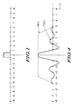
- FIG. 1 is a representation of a rectangular digital prototype pulse or signaling waveform which results in consumption of relatively large amounts of frequency spectrum when modulated on a radio frequency carrier signal.
- FIG. 2A is a graphic representation of a reference pulse exhibiting minimum intersymbol interference.
- FIG. 2B is a representation of a window function applied to the reference pulse to minimize energy outside the window.
- FIG. 2C is a representation of the voltage spectrum derived by taking the Fourier transform of the windowed reference pulse.
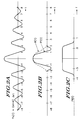
- FIG. 3A is a representation of the voltage spectrum of the reciprocal of the transfer function of a receiver post detection filter.
- FIG. 3B is a representation of the voltage spectrum derived by applying transformed pulse of FIG. 2C to the response derived in FIG. 3A.
- FIG. 3C is a representation of a pre-distorted pulse matching the characteristics of the receiver post detection filter, derived by taking the inverse Fourier transform of the waveform of FIG. 3B.
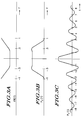
- Figure 4 is a presentation of the final prototype pulse of the present invention derived by windowing the pre-distorted pulse of FIG 3C.
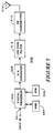
- FIG. 5 is an electrical block diagram of the transmitting apparatus of the present invention.
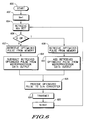
- FIG. 6 is a flow chart of the software program which is stored in memory in the transmitting apparatus of FIG. 5 to govern the operation of such transmitting apparatus.
- FIG. 7 is an electrical block diagram of a conventional FM receiver employed to receive transmissions from the transmitting apparatus of FIG. 5.
- FIG. 8 is a flowchart of the method of the invention.
- the prototype pulse should be compatible with data transmissions over a broad range of data bit rates, such as the 600 bit per second data rate of the POCSAG signaling format, to data bit rates of 4800 and 9600 bits per second, and higher.
- the prototype pulse should be readily detected using conventional FM receivers with simple post detection filtering. The derivation of one embodiment of the prototype pulse of the present invention is shown in FIGS. 2A-2C and 3A-3B.
- FIG. 2A is a graphic representation of the reference pulse P 0 (t) used as the starting point.
- the reference pulse used is the well known sync function (sin ⁇ t)/ ⁇ t which exhibits the desirable characteristic of providing no intersymbol interference.
- the reference pulse represented by the sync function is too complex to use directly, and would also result in the generation of considerable splatter and adjacent channel interference.
- a window function K(t) is applied to the reference pulse P 0 (t) truncating the pulse to a length of from ⁇ 1 second to ⁇ 3.5 seconds.
- the optimum value selected depends on the frequency deviation used in the system. Too short a window increases the spectrum occupied by the baseband signal, resulting in excess splatter in the transmitted signal. Too long a window results in high modulation overshoots, also resulting in excess splatter in the transmitted signal.
- the preferred window function K(t) is a Kaiser window which truncates the reference pulse P 0 (t) to a length of ⁇ 2 seconds. A description of the Kaiser window function may be found in a textbook by Childers and Durling, entitled “Digital Filtering and Signal Processing", published 1975 by West Publishing Company of St. Paul, Minnesota on pages 437 to 440.
- the resultant window reference pulse P 1 (t) is obtained by multiplying the reference pulse P 0 (t) by the window function K(t).
- the voltage spectrum P 1 (f) is determined by taking the Fourier transform of the windowed reference pulse P 1 (t).
- a graphic representation of the voltage spectrum P 1 (f) derived is shown in FIG. 2C.
- the post detection low pass filter used in the receiver is preferably a second order Butterworth filter with a .6 Hz cutoff frequency.
- FIG. 3A A graphic representation of the voltage spectrum of the reciprocal filter function FR(f) is shown in FIG. 3A.
- the voltage spectrum P 2 (f) of the desired prototype pulse P 2 (t) can be determined by mulziplying the voltage spectrum of the filter function FR(f) by the voltage spectrum P 1 (f) of the windowed reference pulse.
- a graphic representation of the voltage spectrum P 2 (f) of the desired prototype pulse is shown in FIG. 3B.
- the desired prototype pulse P 2 (t) in next determined by taking the inverse Fourier transform of the voltage spectrum P 2 (f) of the desired prototype pulse P 2 (t) obtained in FIG 3B.
- a graphic representation of the desired prototype pulse P 2 (t) is shown in FIG. 3C.
- the desired prototype pulse P 2 (t) has been distorted from an ideal (sin ⁇ t)/ ⁇ t function by the process described, resulting in zero crossings to occur at intervals along the time axis which are other then at integer increments, as with the (sin ⁇ t)/ ⁇ t function. Since the distortion imposed was using the reciprocal of the transfer function of the post detection low pass filter, a similar but opposite distortion effect will occur in the receiver, restoring the zero crossings to integer increments in the receiver.
- the desired prototype pulse P 2 (t) as shown in FIG. 3C is too complex for utilization.
- the final step in deriving a final prototype pulse providing the original goals of low splatter and adjacent channel interference, and minimum intersymbol distortion, is shown by the graphic representation illustrated in FIG. 4.
- the final prototype pulse P 3 (t) is determined by applying a second predetermined window function W(t) to truncate the time span of the desired prototype pulse P 2 (t) to a finite length while preserving virtually all of the energy of the pulse.
- the preferred method is to apply a window equal to unity in the region from ⁇ 4 seconds, having cosine squared shaping, which is well known to one of ordinary skill in the art, in the regions -5 to -4 and +4 to +5 seconds, and thereafter being zero outside of ⁇ 5 seconds.
- a graphic representation of the final prototype pulse P 3 (t) is shown in FIG. 4, and was obtained by multiplying the desired prototype pulse P 2 (t) by the second window function W(t).
- the final prototype pulse P 3 (t) has the characteristics of providing low splatter and adjacent channel interference during transmission, and minimum intersymbol distortion when being detected in the receiver.
- the derivation obtained was for a pulse normalized for 1 symbol/second. It will be appreciated that the result obtained may be scaled for a wide range of data bit rates.
- the time indicated scales down and frequency scales up as the data bit rate is increased.
- FIG. 5 is an electrical block diagram of the transmitting apparatus of the present invention.
- the heart of the transmitting apparatus is a digital processor 502, such as a DSP 56000 digital signal processor integrated circuit manufactured by Motorola, Inc. Coupled to the digital processor 502, is a random access memory (RAM) 504 and a read only memory (ROM) 506.
- RAM 504 provides temporary storage for digital processor 502.
- Numerical values of the final prototype pulse P 3 (t), previously described, are stored in ROM 506.
- the final prototype pulse P 3 (t) is sampled from ROM 506 at a rate consistent with the rate at which data is input at digital processor input 501.
- the data input is a stream of binary information corresponding to the receiver addresses and messages desired to be transmitted.
- the sampled values of the prototype pulse are multiplied by a constant which depends on the data to be transmitted and each in turn is added to the output stream.
- the constants are, for example, +1 to send a logic one, and -1 to send a logic zero. This would result in transmitting the prototype pulse to represent a logic one, and the negative of the prototype pulse to represent a logic zero.
- the method is easily extended to multilevel transmission. For example, constants of -1, -.333, +.333, and +1 could be used for four-level transmission.
- the stream of prototype pulse data is converted to analog form by digital to analog (D/A) converter 508, such as an MC145040 D/A converter manufactured by Motorola, Inc.
- D/A converter 508 is then filtered by low pass filter 510 to eliminate the spurious signals which arise in the digital to analog conversion process.
- the design of low pass filters to eliminate the spurious signals arising in the digital to analog conversion process are well known in the art.
- the resulting baseband modulating signal at the output of the low pass filter 510 is used as the modulating signal for a conventional FM transmitter 512.
- FIG. 6 is a flowchart of the software program which is employed to govern the operation of'digital processor 502 in accordance with the present invention.
- Such software program is stored in ROM 506.
- the operational routine begins at block 600 at which the system is initialized.
- N is defined to be an index number which corresponds to each of the bits of data which are to be transmitted by transmitter 512. For example, for the first bit of data at data input 501 which is to be transmitted, N is defined to be equal to one. For the second bit of such data, N equals 2 and so forth.
- Flow continues to block 602 at which N, the number of the data input bit, is set to equal 1.
- the samples of the optimized pulse are then provided the D/A converter 508, at block 616 at which such samples are converted into an analog reproduction of the optimized pulse.
- the reconstructed optimized pulse is then transmitted by transmitter 512, as per block 618, after being suitably filtered by low pass filter 510.
- FIG. 7 is an electrical block diagram of the conventional receiver employed to receive the transmissions from the transmitting apparatus of FIG. 5.
- the transmitted stream of optimized prototype pulse signals is intercepted by antenna 702 and received by FM receiver 704.
- FM receiver 704 is a conventional FM receiver which is well known in the art, and utilizes any of a number of well known demodulator circuits, such as pulse count discriminators and peak and valley detectors, for the detection of the received FM signals.
- the output from FM receiver 704 is a waveform stream characteristic of the transmitted optimized prototype pulse signals generated to represent the binary information pattern desired to be transmitted. As previously described, these optimized prototype pulse signals have been pre-distorted from an ideal (sin ⁇ t) ⁇ t function waveform, by the processing that occurred at the transmitting apparatus 500.
- the output of FM receiver 704 is coupled to post detection low pass filter 706 which is preferably a second order Butterworth filter with a .6 Hz cutoff frequency for data normalized to 1 symbol/second.
- Post detection low pass filter 706 filters out the excess discriminator noise, and distorts the recovered waveform so that zero crossings of each transmitted pulse occur at integer intervals of time, restoring the characteristic of having no intersymbol interference in the recovered signals.
- the output of post detection low pass filter 706 is coupled to a clock recovery circuit 708 which is used to obtain bit synchronization from the recovered data signal in a manner well known to one of ordinary skill in the art.
- the clock recovery circuit 708 controls sampling the output of the post detection low pass filter 706. The sampling function is indicated by switch 710.
- Bit decisions are based on the amplitude of each sampled bit.
- a logical one is generated at the output of comparator 712.
- a logical zero is generated at the output of comparator 712.
- the method of generating an optimized prototype pulse is summarized in the flowchart of FIG. 8.
- the selected function is windowed at bloc 804, by a predetermined window function to obtain a pulse P 1 (t) having minimum energy outside the window.
- the voltage spectrum P 1 (f) of the pulse P 1 (t) derived at step 804, is determined by taking the Fourier transform at step 806.
- the reciprocal transfer function FR(f) of the receiver post detection low pass filter is determined at step 808.
- the reciprocal transfer function FR(f) is multiplied by the voltage spectrum P 1 (f) to determine the voltage spectrum P 2 (f) at block 810.
- the desired prototype pulse is determined, at step 812, by taking the inverse Fourier transform of the voltage spectrum P 2 (f).
- the optimized prototype pulse is finally determined by windowing the desired prototype pulse with a second predetermined window function, at step 814.
- Data defining the optimized prototype pulse is stored in a ROM, to be used in the transmission of binary information.
- the optimized prototype pulse minimizes splatter and adjacent channel interference.
- the transmitted optimized prototype pulses can be recovered by a conventional FM receiver, with no generation of intersymbol interference in the process.
Landscapes
- Engineering & Computer Science (AREA)
- Physics & Mathematics (AREA)
- Spectroscopy & Molecular Physics (AREA)
- Power Engineering (AREA)
- Computer Networks & Wireless Communication (AREA)
- Signal Processing (AREA)
- Digital Transmission Methods That Use Modulated Carrier Waves (AREA)
- Stereo-Broadcasting Methods (AREA)
- Transmitters (AREA)
- Dc Digital Transmission (AREA)
Abstract
Description
- This invention relates generally to the field of communications systems, and more particularly to a communication system providing a spectrally efficient digital FM modulation system for use with a conventional frequency modulated (FM) receiver.
- A number of problems exist with digital frequency modulated (FM) transmission systems. One such problem relates to splatter and adjacent channel interference created when rectangular pulses, such as found in strings of digital information, is transmitted. It is well known that this splatter is reduced by low pass filtering the baseband modulating signal. Many waveshaping functions are known which minimize the spectrum occupied by the baseband modulating signal. Unfortunately, in an FM system, minimal occupied baseband spectrum does not imply minimal occupied radio frequency (RF) spectrum. Many of the well known waveshaping functions produce high modulation overshoots which result in excessive splatter, even though the baseband frequency spectrum is well contained. A means of reliably minimizing the splatter of the transmitted RF signal, considering both baseband spectrum and modulation overshoots is required.
- A second problem occurring in digital FM modulated transmission systems is the generation of intersymbol interference in the received signal. In general, this is caused by the waveshaping which is required to reduce splatter. When waveshaping is employed, each transmitted bit becomes spread out in time over several adjacent bits resulting in interference during the detection of these bits. Intersymbol interference results in a sensitivity loss in the receiver. Only certain classes of shaped signals are known to exhibit no intersymbol interference. However, most of these shaped signals are extremely complex in structure. A means of adapting one or more of these shaped signals is required if intersymbol interference is to be minimized.
- When such complex shaped signals are used, very complicated analog filters are required in the receiver to obtain the low intersymbol interference inherent in the signal. A means is required to adapt these complex shaped signals for use in receivers using conventional post detection filtering commonly found in the FM receivers, such as pagers, which are in wide use today.
- Many FM modulation systems also place constraints on the bit rate at which digital data can be transmitted. Any method which reduces splatter while minimizing intersymbol interference should not unduly restrict the maximum bit rate which can be transmitted in a given RF channel.
- US Patent No. 4,737,969 discloses a method for generating a uniquely shaped prototype digital pulse which is transmitted with minimal frequency spectrum consumption and yet a relatively high bit rate. Such uniquely shaped digital pulse is stored in a memory included in a transmitter until transmission is desired, at which time a positive of the pulse is transmitted to correspond to a first logic level or the negative of the pulse is transmitted to correspond to a second logic level.
- It is an object of the present invention to provide a communication system providing spectrally efficient data transmission over a broad range of data transmission rates.
- It is a further object of the present invention to provide a communication system which minimizes adjacent channel splatter over the broad range of data transmission rates.
- It is a further object of the present invention to provide a communication which minimizes received intersymbol interference over the broad range of data transmission rates.
- It is a further object of the present invention to provide a communication system which utilizes a conventional frequency modulated (FM) receiver for the reception of the broad range of data transmission rates.
- In accordance with a first aspect of the present invention there is provided a method for generating an optimized electric pulse which is used in the transmission of information to a frequency modulated (FM) receiver for minimizing intersymbol interference as recited in
claim 1. - In accordance with a second aspect of the present invention there is provided a method for transmitting digital information to a communication receiver employing a post detection low pass filter having a predetermined filter transfer function using an optimized electric pulse as recited in
claim 4. - In accordance with a third aspect of the present invention there is provided a transmitter for transmitting digital information to a communication receiver employing a post detection low pass filter having a predetermined filter transfer function using an optimized electric pulse as recited in
claim 9. - A method is described for transmitting digital data with minimum splatter and for recovering the same with a conventional frequency modulated (FM) receiver to obtain data having minimum intersymbol interference. The method utilizes a optimized prototype pulse which has been pre-distorted to match the inverse characteristics of the post detection low pass filter in a conventional FM receiver.
- The features of the invention are set forth with particularity in the appended claims. The invention itself, together with its further objects and advantages thereof, may be best understood by reference to the following description when taken in conjunction with the accompanying drawings, in the several figures of which like reference numerals identify identical elements, in which, and wherein:
- FIG. 1 is a representation of a rectangular digital prototype pulse or signaling waveform which results in consumption of relatively large amounts of frequency spectrum when modulated on a radio frequency carrier signal.
- FIG. 2A is a graphic representation of a reference pulse exhibiting minimum intersymbol interference.
- FIG. 2B is a representation of a window function applied to the reference pulse to minimize energy outside the window.
- FIG. 2C is a representation of the voltage spectrum derived by taking the Fourier transform of the windowed reference pulse.
- FIG. 3A is a representation of the voltage spectrum of the reciprocal of the transfer function of a receiver post detection filter.
- FIG. 3B is a representation of the voltage spectrum derived by applying transformed pulse of FIG. 2C to the response derived in FIG. 3A.
- FIG. 3C is a representation of a pre-distorted pulse matching the characteristics of the receiver post detection filter, derived by taking the inverse Fourier transform of the waveform of FIG. 3B.
- Figure 4 is a presentation of the final prototype pulse of the present invention derived by windowing the pre-distorted pulse of FIG 3C.
- FIG. 5 is an electrical block diagram of the transmitting apparatus of the present invention.
- FIG. 6 is a flow chart of the software program which is stored in memory in the transmitting apparatus of FIG. 5 to govern the operation of such transmitting apparatus.
- FIG. 7 is an electrical block diagram of a conventional FM receiver employed to receive transmissions from the transmitting apparatus of FIG. 5.
- FIG. 8 is a flowchart of the method of the invention.
- To facilitate an understanding of the present invention, a discussion of the method of generating a digital pulse which is optimized both in terms of the time domain (bit rate, pulse duration) and frequency domain (frequency consumed) ensues. For purposes of this example, it is assumed that digital pulses normalized to 1 bit/sec such as the pulse illustrated in FIG. 1, are desired to be transmitted. If a series of such nearly square wave or rectangular pulses were modulated on an electromagnetic carrier wave, the sharp transistions in such pulses would result in the consumption of an unduly large amount of frequency spectrum. This is not acceptable given the bandwidth constraints which are imposed by modern communication systems.
- It is desirable to produce a prototype pulse which, when transmitted, minimizes the splatter and adjacent channel interference. The prototype pulse should be compatible with data transmissions over a broad range of data bit rates, such as the 600 bit per second data rate of the POCSAG signaling format, to data bit rates of 4800 and 9600 bits per second, and higher. The prototype pulse should be readily detected using conventional FM receivers with simple post detection filtering. The derivation of one embodiment of the prototype pulse of the present invention is shown in FIGS. 2A-2C and 3A-3B.
- FIG. 2A is a graphic representation of the reference pulse P0(t) used as the starting point. The reference pulse used is the well known sync function (sin πt)/πt which exhibits the desirable characteristic of providing no intersymbol interference. The reference pulse represented by the sync function is too complex to use directly, and would also result in the generation of considerable splatter and adjacent channel interference.
- As shown in FIG. 2B, a window function K(t) is applied to the reference pulse P0(t) truncating the pulse to a length of from ±1 second to ± 3.5 seconds. The optimum value selected depends on the frequency deviation used in the system. Too short a window increases the spectrum occupied by the baseband signal, resulting in excess splatter in the transmitted signal. Too long a window results in high modulation overshoots, also resulting in excess splatter in the transmitted signal. The preferred window function K(t) is a Kaiser window which truncates the reference pulse P0(t) to a length of ± 2 seconds. A description of the Kaiser window function may be found in a textbook by Childers and Durling, entitled "Digital Filtering and Signal Processing", published 1975 by West Publishing Company of St. Paul, Minnesota on pages 437 to 440.
- The resultant window reference pulse P1(t) is obtained by multiplying the reference pulse P0(t) by the window function K(t).
- Once the windowed reference pulse has been determined, as described, the voltage spectrum P1(f) is determined by taking the Fourier transform of the windowed reference pulse P1(t). A graphic representation of the voltage spectrum P1(f) derived is shown in FIG. 2C.
- The next step in determining the final prototype pulse is to determine the filter function FR(f) which is the reciprocal of the transfer function of the post detection low pass filter utilized in the receiver of the preferred embodiment of the present invention. That is, FR(f) = 1/H(f) for all values of f, where H(f) is the transfer function of the receiver post detection filter. For optimum detection characteristics in the receiver, the post detection low pass filter used in the receiver is preferably a second order Butterworth filter with a .6 Hz cutoff frequency. A graphic representation of the voltage spectrum of the reciprocal filter function FR(f) is shown in FIG. 3A. From the reciprocal filter function FR(f), the voltage spectrum P2(f) of the desired prototype pulse P2(t) can be determined by mulziplying the voltage spectrum of the filter function FR(f) by the voltage spectrum P1(f) of the windowed reference pulse. A graphic representation of the voltage spectrum P2(f) of the desired prototype pulse is shown in FIG. 3B. The desired prototype pulse P2(t) in next determined by taking the inverse Fourier transform of the voltage spectrum P2(f) of the desired prototype pulse P2(t) obtained in FIG 3B. A graphic representation of the desired prototype pulse P2(t) is shown in FIG. 3C. It should be noted that the desired prototype pulse P2(t) has been distorted from an ideal (sin πt)/πt function by the process described, resulting in zero crossings to occur at intervals along the time axis which are other then at integer increments, as with the (sin πt)/πt function. Since the distortion imposed was using the reciprocal of the transfer function of the post detection low pass filter, a similar but opposite distortion effect will occur in the receiver, restoring the zero crossings to integer increments in the receiver.
- The desired prototype pulse P2(t) as shown in FIG. 3C is too complex for utilization. The final step in deriving a final prototype pulse providing the original goals of low splatter and adjacent channel interference, and minimum intersymbol distortion, is shown by the graphic representation illustrated in FIG. 4. The final prototype pulse P3(t) is determined by applying a second predetermined window function W(t) to truncate the time span of the desired prototype pulse P2(t) to a finite length while preserving virtually all of the energy of the pulse. The preferred method is to apply a window equal to unity in the region from ±4 seconds, having cosine squared shaping, which is well known to one of ordinary skill in the art, in the regions -5 to -4 and +4 to +5 seconds, and thereafter being zero outside of ±5 seconds. A graphic representation of the final prototype pulse P3(t) is shown in FIG. 4, and was obtained by multiplying the desired prototype pulse P2(t) by the second window function W(t).
- To summarize, a method of mathematically deriving a final prototype pulse P3(t) has been illustrated in FIGS. 2A-2C, 3A-3C, and 4. The final prototype pulse P3(t) has the characteristics of providing low splatter and adjacent channel interference during transmission, and minimum intersymbol distortion when being detected in the receiver. As previously described, the derivation obtained was for a pulse normalized for 1 symbol/second. It will be appreciated that the result obtained may be scaled for a wide range of data bit rates. When scaling the final prototype pulse to other data bit rates, it will be appreciated that the time indicated scales down and frequency scales up as the data bit rate is increased.
- Figure 5 is an electrical block diagram of the transmitting apparatus of the present invention. The heart of the transmitting apparatus is a
digital processor 502, such as a DSP 56000 digital signal processor integrated circuit manufactured by Motorola, Inc. Coupled to thedigital processor 502, is a random access memory (RAM) 504 and a read only memory (ROM) 506.RAM 504 provides temporary storage fordigital processor 502. Numerical values of the final prototype pulse P3(t), previously described, are stored inROM 506. The final prototype pulse P3(t) is sampled fromROM 506 at a rate consistent with the rate at which data is input atdigital processor input 501. The data input is a stream of binary information corresponding to the receiver addresses and messages desired to be transmitted. For each transmitted symbol, the sampled values of the prototype pulse, in sequence, are multiplied by a constant which depends on the data to be transmitted and each in turn is added to the output stream. The constants are, for example, +1 to send a logic one, and -1 to send a logic zero. This would result in transmitting the prototype pulse to represent a logic one, and the negative of the prototype pulse to represent a logic zero. The method is easily extended to multilevel transmission. For example, constants of -1, -.333, +.333, and +1 could be used for four-level transmission. - The stream of prototype pulse data is converted to analog form by digital to analog (D/A)
converter 508, such as an MC145040 D/A converter manufactured by Motorola, Inc. The output of D/A converter 508 is then filtered bylow pass filter 510 to eliminate the spurious signals which arise in the digital to analog conversion process. The design of low pass filters to eliminate the spurious signals arising in the digital to analog conversion process are well known in the art. The resulting baseband modulating signal at the output of thelow pass filter 510 is used as the modulating signal for aconventional FM transmitter 512. - FIG. 6 is a flowchart of the software program which is employed to govern the
operation of'digital processor 502 in accordance with the present invention. Such software program is stored inROM 506. As seen in FIG. 6, the operational routine begins atblock 600 at which the system is initialized. N is defined to be an index number which corresponds to each of the bits of data which are to be transmitted bytransmitter 512. For example, for the first bit of data atdata input 501 which is to be transmitted, N is defined to be equal to one. For the second bit of such data, N equals 2 and so forth. Flow continues to block 602 at which N, the number of the data input bit, is set to equal 1. Atblock 604,digital processor 502 reads the first bit (N=1) of data fromdata input 501.Digital processor 502 then determines whether such first bit is a logical 0 or 1 atdecision block 606. If the first bit (N=l) is determined to be a logical 1, thendigital processor 502 retrieves the samples of the optimized pulse stored inROM 506, atblock 608, and adds such samples, atblock 610, to the output ofdigital processor 502. If, however, the first bit (N=1) is determined to be a logical 0, thedigital processor 502 retrieves the samples of the optimized pulse stored inROM 506, atblock 612, and subtracts such samples from the output ofdigital processor 502, atblock 614. In either case, the samples of the optimized pulse (whether the positive or the negative thereof) are then provided the D/A converter 508, atblock 616 at which such samples are converted into an analog reproduction of the optimized pulse. The reconstructed optimized pulse is then transmitted bytransmitter 512, as perblock 618, after being suitably filtered bylow pass filter 510.Digital processor 502, atblock 620, then advances the N counter to the next bit of input data (N=2) such that thedigital processor 502 reads the second bit atblock 604 and processes such second bit as described above. Process flow continues in a substantially similar manner for the subsequent bits N=3,4.... - Figure 7 is an electrical block diagram of the conventional receiver employed to receive the transmissions from the transmitting apparatus of FIG. 5. The transmitted stream of optimized prototype pulse signals is intercepted by
antenna 702 and received byFM receiver 704.FM receiver 704 is a conventional FM receiver which is well known in the art, and utilizes any of a number of well known demodulator circuits, such as pulse count discriminators and peak and valley detectors, for the detection of the received FM signals. The output fromFM receiver 704 is a waveform stream characteristic of the transmitted optimized prototype pulse signals generated to represent the binary information pattern desired to be transmitted. As previously described, these optimized prototype pulse signals have been pre-distorted from an ideal (sin πt)πt function waveform, by the processing that occurred at the transmittingapparatus 500. The output ofFM receiver 704 is coupled to post detectionlow pass filter 706 which is preferably a second order Butterworth filter with a .6 Hz cutoff frequency for data normalized to 1 symbol/second. Post detectionlow pass filter 706 filters out the excess discriminator noise, and distorts the recovered waveform so that zero crossings of each transmitted pulse occur at integer intervals of time, restoring the characteristic of having no intersymbol interference in the recovered signals. The output of post detectionlow pass filter 706 is coupled to aclock recovery circuit 708 which is used to obtain bit synchronization from the recovered data signal in a manner well known to one of ordinary skill in the art. Theclock recovery circuit 708 controls sampling the output of the post detectionlow pass filter 706. The sampling function is indicated byswitch 710. Bit decisions are based on the amplitude of each sampled bit. When the recovered signal is positive, indicating the transmission of the optimized prototype pulse signal, a logical one is generated at the output ofcomparator 712. When the recovered signal is negative, indicating the transmission of the inverse of the optimized prototype pulse signal, a logical zero is generated at the output ofcomparator 712. There is no intersymbol distortion in this decision process, except that which is unavoidable due to the IF filtering and that caused by multipath signal reception. - The method of generating an optimized prototype pulse is summarized in the flowchart of FIG. 8. The method starts with a function P0(t) = (sin πt)/πt at
block 802. The selected function is windowed atbloc 804, by a predetermined window function to obtain a pulse P1(t) having minimum energy outside the window. The voltage spectrum P1(f) of the pulse P1(t) derived atstep 804, is determined by taking the Fourier transform atstep 806. The reciprocal transfer function FR(f) of the receiver post detection low pass filter is determined atstep 808. The reciprocal transfer function FR(f) is multiplied by the voltage spectrum P1(f) to determine the voltage spectrum P2(f) atblock 810. The desired prototype pulse is determined, atstep 812, by taking the inverse Fourier transform of the voltage spectrum P2(f). The optimized prototype pulse is finally determined by windowing the desired prototype pulse with a second predetermined window function, atstep 814. Data defining the optimized prototype pulse is stored in a ROM, to be used in the transmission of binary information. When transmitted, the optimized prototype pulse minimizes splatter and adjacent channel interference. The transmitted optimized prototype pulses can be recovered by a conventional FM receiver, with no generation of intersymbol interference in the process.
Claims (10)
- A method for generating an optimized electric pulse for use in the transmission of information to a frequency modulated (FM) receiver (700) for minimizing intersymbol interference, said method comprising the steps of:selecting a first pulse Po(t) = (sin πt)/πt which exhibits the property of low intersymbol interference (FIG. 2A);multiplying the first pulse Po(t) with a first predetermined window function K(t) to obtain a second pulse P1(t) minimizing the energy density outside the window (FIG. 2B); anddetermining the spectrum P1(f) by taking the Fourier transform of the second pulse P1(t) (FIG. 2C);said method being CHARACTERIZED BY THE STEPS OF:determining a filter function FR(f) which is the reciprocal of the transfer function of the receiver post detection low pass filter (FIG. 3A);multiplying the spectrum P1(f) with the reciprocal filter function FR(f) to obtain a spectrum P2(f) (FIG. 3B);determining a third pulse P2(t) by taking the inverse Fourier transform of the spectrum P2(f) (FIG. 3C); andmultiplying the third pulse P2(t) by a second predetermined window function W(t) to truncate the time span of pulse P2(t) to a finite length which substantially preserves the energy of the pulse P2(t) to obtain the optimized electric pulse P3(t) (FIG. 4).
- The method for generating an optimized electric pulse, according to claim 1 wherein the first predetermined window function K(t) is a Kaiser window function.
- The method for generating an optimized electric pulse, according to claim 1 or 2 wherein the second predetermined window function (W(t) is a unity window function having cosine squared shaping.
- A method for transmitting digital information to a communication receiver (700) employing a post detection low pass filter (706) having predetermined filter transfer function using an optimized, electric pulse, said method for transmitting comprising the steps of:storing the optimized electric pulse which is derived by processing an electric pulse obtained via the method of Claims 1, 2, or 3, the optimized electric pulse when received and processed by the post detection low pass filter (706) of the communication receiver (700) providing a pulse shape exhibiting minimal intersymbol interference;recovering the stored, optimized electric pulse in response to the digital information to be transmitted, for generating a sequence of the optimized electric pulses corresponding thereto; andtransmitting the sequence of optimized electric pulses.
- The method according to claim 4, wherein said step of storing comprises the step of storing a sequence of numerical values depicting the optimized electric pulse.
- The method according to claim 5, wherein the digital information is represented by at least two transmitted symbols, and wherein said step of generating comprises the steps of:selecting the sequence of numerical values depicting the optimized electric pulse corresponding to the first transmitted symbol; andselecting the inverse of the sequence of numerical values depicting the optimized electric pulse corresponding to the second transmitted symbol.
- The method according to claim 6, wherein said step of generating further comprises the steps of:converting the sequences of numerical values depicting the optimized electric pulses and the inverses into an analog sequence of optimized electric pulses and the inverses corresponding to the digital information to be transmitted; andfiltering the analog sequence of optimized electric pulses and the inverses.
- The method according to claim 7, wherein said step of transmitting further comprises the step of transmitting the filtered analog sequence of optimized electric pulses and the inverses.
- A transmitter for transmitting digital information to a communication receiver employing a post detection low pass filter having a predetermined filter transfer function using an optimized electric pulse, said transmitter comprising:means for storing (506) a sequence of numerical values depicting the optimized electric pulse, the sequence of numerical values being derived by processing an electric pulse obtained via the method of Claims 1, 2, or 3, the optimized electric pulse when received and processed by the post-detection low pass filter (706) of the communication receiver (700) providing a pulse shape exhibiting minimal intersymbol interference;means for receiving (501) the digital information depicting a message;means, responsive to the digital information received, for recovering (502) the sequence of numerical values depicting the optimized electric pulse from said storing means (506), and therefrom generating a sequence of optimized electric pulses depicting the digital message; andmeans for transmitting (512) the sequence of optimized electric pulses.
- The transmitter according to claim 9, wherein said means for storing (506) comprises a read only memory.
Applications Claiming Priority (3)
| Application Number | Priority Date | Filing Date | Title |
|---|---|---|---|
| US390317 | 1989-08-07 | ||
| US07/390,317 US5068874A (en) | 1989-08-07 | 1989-08-07 | Spectrally efficient digital fm modulation system |
| PCT/US1990/003790 WO1991002403A1 (en) | 1989-08-07 | 1990-07-09 | Spectrally efficient digital fm modulation system |
Publications (3)
| Publication Number | Publication Date |
|---|---|
| EP0572376A4 EP0572376A4 (en) | 1992-10-03 |
| EP0572376A1 EP0572376A1 (en) | 1993-12-08 |
| EP0572376B1 true EP0572376B1 (en) | 1997-03-12 |
Family
ID=23542009
Family Applications (1)
| Application Number | Title | Priority Date | Filing Date |
|---|---|---|---|
| EP90911006A Expired - Lifetime EP0572376B1 (en) | 1989-08-07 | 1990-07-09 | Spectrally efficient digital fm modulation system |
Country Status (6)
| Country | Link |
|---|---|
| US (1) | US5068874A (en) |
| EP (1) | EP0572376B1 (en) |
| JP (1) | JP2564992B2 (en) |
| AT (1) | ATE150233T1 (en) |
| DE (1) | DE69030198T2 (en) |
| WO (1) | WO1991002403A1 (en) |
Families Citing this family (21)
| Publication number | Priority date | Publication date | Assignee | Title |
|---|---|---|---|---|
| SE468616B (en) * | 1991-06-12 | 1993-02-15 | Ericsson Telefon Ab L M | PROCEDURE FOR COMPENSATION OF THE TRANSMITTER USE SIGNAL'S DEPENDENCE OF THE TRANSFER FUNCTION FOR A COMBINER FILTER |
| US5412691A (en) * | 1991-06-28 | 1995-05-02 | Digital Equipment Corporation | Method and apparatus for equalization for transmission over a band-limited channel |
| US5177768A (en) * | 1991-11-22 | 1993-01-05 | Bell Communications Research, Inc. | Spread-time code division multiple access technique with arbitrary spectral shaping |
| US5173923A (en) * | 1991-11-22 | 1992-12-22 | Bell Communications Research, Inc. | Spread-time code division multiple access technique with arbitrary spectral shaping |
| US5175743A (en) * | 1991-11-22 | 1992-12-29 | Bell Communications Research, Inc. | Spread-time code division multiple access technique with arbitrary spectral shaping |
| US5175744A (en) * | 1991-11-22 | 1992-12-29 | Bell Communications Research, Inc. | Spread-time code division multiple access technique with arbitrary spectral shaping |
| US5287387A (en) * | 1992-03-06 | 1994-02-15 | Motorola, Inc. | Low splatter peak-to-average signal reduction |
| CH684860A5 (en) * | 1992-04-23 | 1995-01-13 | Haeni Prolectron Ag | Method and circuit for the transmission of binary data sequences. |
| US5657353A (en) * | 1992-12-31 | 1997-08-12 | Stellar One Corporation | Pulse shaping filter for received digital transmissions using phase lock loop for adjusting shift register |
| US5638404A (en) * | 1994-09-22 | 1997-06-10 | Her Majesty The Queen In Right Of Canada, As Represented By The Minister Of Communications | Pre-compensated frequency modulation (PFM) |
| US5579342A (en) * | 1994-09-22 | 1996-11-26 | Her Majesty The Queen In Right Of Canada As Represented By The Minister Of Communications | Pre-compensated frequency modulation (PFM) |
| US5633893A (en) * | 1994-09-29 | 1997-05-27 | Ericsson Inc. | Digital modulation method with controlled envelope variation |
| TW318297B (en) * | 1995-05-22 | 1997-10-21 | Motorola Inc | |
| WO1997035210A1 (en) * | 1996-03-20 | 1997-09-25 | Radian International L.L.C. | Digitally-controlled pulse shaper for pulsed radar systems and radar wind profilers |
| US6137831A (en) * | 1997-06-20 | 2000-10-24 | Johnson; Neldon P. | Method and apparatus for reducing receiver imposed distortion |
| WO1999062207A1 (en) * | 1998-05-26 | 1999-12-02 | Jean Armstrong | Data transmission and reception in multicarrier modulation systems |
| US6405147B1 (en) * | 1999-09-10 | 2002-06-11 | Condor Systems, Inc. | Signal transfer device measurement system and method |
| US6876697B2 (en) * | 2000-12-12 | 2005-04-05 | Sierra Wireless, Inc. | Apparatus and method for power ramp up of wireless modem transmitter |
| US7349489B2 (en) | 2001-08-13 | 2008-03-25 | Nokia Siemens Networks Gmbh & Co. Kg | Pulse shaping filter with minimal intersymbol interference |
| US20030108110A1 (en) * | 2001-12-10 | 2003-06-12 | The Boeing Company | Systems and methods for reducing electromagnetic emissions in communications |
| US10915353B2 (en) | 2019-04-01 | 2021-02-09 | International Business Machines Corporation | Intelligent processor for user-provided routines in a transaction processing system |
Family Cites Families (8)
| Publication number | Priority date | Publication date | Assignee | Title |
|---|---|---|---|---|
| US4123755A (en) * | 1975-10-10 | 1978-10-31 | William Fishbein | Radar interference reduction |
| US4135057A (en) * | 1976-09-07 | 1979-01-16 | Arthur A. Collins, Inc. | High density digital transmission system |
| JPS5717027A (en) * | 1980-07-03 | 1982-01-28 | Hitachi Ltd | Vibration reducing device of electric machinery |
| US4412337A (en) * | 1981-11-04 | 1983-10-25 | Motorola Inc. | Power amplifier and envelope correction circuitry |
| US4507794A (en) * | 1983-05-04 | 1985-03-26 | Jones Stephen K | Filtered Manchester Coded PSK transmission system |
| US4718093A (en) * | 1984-03-27 | 1988-01-05 | Exxon Research And Engineering Company | Speech recognition method including biased principal components |
| US4694468A (en) * | 1986-04-25 | 1987-09-15 | Eastman Kodak Company | Apparatus useful in channel equalization adjustment |
| US4737969A (en) * | 1987-01-28 | 1988-04-12 | Motorola, Inc. | Spectrally efficient digital modulation method and apparatus |
-
1989
- 1989-08-07 US US07/390,317 patent/US5068874A/en not_active Expired - Lifetime
-
1990
- 1990-07-09 JP JP2510392A patent/JP2564992B2/en not_active Expired - Lifetime
- 1990-07-09 WO PCT/US1990/003790 patent/WO1991002403A1/en not_active Ceased
- 1990-07-09 DE DE69030198T patent/DE69030198T2/en not_active Expired - Fee Related
- 1990-07-09 EP EP90911006A patent/EP0572376B1/en not_active Expired - Lifetime
- 1990-07-09 AT AT90911006T patent/ATE150233T1/en not_active IP Right Cessation
Also Published As
| Publication number | Publication date |
|---|---|
| DE69030198D1 (en) | 1997-04-17 |
| EP0572376A4 (en) | 1992-10-03 |
| US5068874A (en) | 1991-11-26 |
| DE69030198T2 (en) | 1997-10-02 |
| JP2564992B2 (en) | 1996-12-18 |
| JPH05501179A (en) | 1993-03-04 |
| EP0572376A1 (en) | 1993-12-08 |
| ATE150233T1 (en) | 1997-03-15 |
| WO1991002403A1 (en) | 1991-02-21 |
Similar Documents
| Publication | Publication Date | Title |
|---|---|---|
| EP0572376B1 (en) | Spectrally efficient digital fm modulation system | |
| EP0345282B1 (en) | Spectrally efficient digital modulation method and apparatus | |
| DE69429779T2 (en) | DIGITAL COMMUNICATION DEVICE USING A FOUR-POINT DIFFERENTIAL FREQUENCY REVERSE | |
| EP1617613B1 (en) | OFDM communication devices using pseudo random modulated reference symbols | |
| EP0702475B1 (en) | Multi-threshold detection for 0.3-GMSK | |
| Aisbett | Automatic modulation recognition using time domain parameters | |
| US5386495A (en) | Method and apparatus for determining the signal quality of a digital signal | |
| US5202900A (en) | Spectrally efficient digital FM modulated transmitter | |
| WO1984004860A1 (en) | Data detector using probabilistic information in received signals | |
| US5274672A (en) | Optimized clock recovery for an MSK system | |
| CN1123586A (en) | A demodulator for frequency shift keyed signals | |
| US20030157905A1 (en) | Transmitter and associated method for reducing the adjacent channel power during wireless communications | |
| US7142613B2 (en) | Methods, systems and devices for generating pulse shapes | |
| US4825452A (en) | Digital FSK demodulator | |
| EP1228614A1 (en) | Method and apparatus for communication using pulse decoding | |
| US7653144B2 (en) | Gaussian FSK modulation with more than two modulation states | |
| US4577335A (en) | Coherent data communications technique | |
| CA1162620A (en) | Method and apparatus for converting binary information into a single-sideband 3-level correlative signal | |
| WO1996037977A1 (en) | Method and apparatus in a communication system for receiving a distorted signal | |
| KR19990082417A (en) | Coherent modulation of the CPM signal | |
| Webber et al. | Implementing a/4 shift D-QPSK baseband modem using the TMS320C50 | |
| US5729575A (en) | Transmitter and receiver system and method utilizing a pilot carrier notch data encoded signal | |
| Salz | Performance of multilevel narrow-band FM digital communication systems | |
| Udawant et al. | Digital image processing by using GMSK | |
| Cox | Error performance bounds for M-ary digital FM with predetection sampling |
Legal Events
| Date | Code | Title | Description |
|---|---|---|---|
| PUAI | Public reference made under article 153(3) epc to a published international application that has entered the european phase |
Free format text: ORIGINAL CODE: 0009012 |
|
| 17P | Request for examination filed |
Effective date: 19920302 |
|
| AK | Designated contracting states |
Kind code of ref document: A1 Designated state(s): AT BE CH DE DK ES FR GB IT LI LU NL SE |
|
| 17Q | First examination report despatched |
Effective date: 19941109 |
|
| GRAG | Despatch of communication of intention to grant |
Free format text: ORIGINAL CODE: EPIDOS AGRA |
|
| GRAH | Despatch of communication of intention to grant a patent |
Free format text: ORIGINAL CODE: EPIDOS IGRA |
|
| GRAH | Despatch of communication of intention to grant a patent |
Free format text: ORIGINAL CODE: EPIDOS IGRA |
|
| GRAA | (expected) grant |
Free format text: ORIGINAL CODE: 0009210 |
|
| ITF | It: translation for a ep patent filed | ||
| AK | Designated contracting states |
Kind code of ref document: B1 Designated state(s): AT BE CH DE DK ES FR GB IT LI LU NL SE |
|
| PG25 | Lapsed in a contracting state [announced via postgrant information from national office to epo] |
Ref country code: NL Free format text: LAPSE BECAUSE OF FAILURE TO SUBMIT A TRANSLATION OF THE DESCRIPTION OR TO PAY THE FEE WITHIN THE PRESCRIBED TIME-LIMIT Effective date: 19970312 Ref country code: LI Effective date: 19970312 Ref country code: ES Free format text: THE PATENT HAS BEEN ANNULLED BY A DECISION OF A NATIONAL AUTHORITY Effective date: 19970312 Ref country code: DK Effective date: 19970312 Ref country code: CH Effective date: 19970312 Ref country code: BE Effective date: 19970312 Ref country code: AT Effective date: 19970312 |
|
| REF | Corresponds to: |
Ref document number: 150233 Country of ref document: AT Date of ref document: 19970315 Kind code of ref document: T |
|
| REG | Reference to a national code |
Ref country code: CH Ref legal event code: EP |
|
| ET | Fr: translation filed | ||
| REF | Corresponds to: |
Ref document number: 69030198 Country of ref document: DE Date of ref document: 19970417 |
|
| PG25 | Lapsed in a contracting state [announced via postgrant information from national office to epo] |
Ref country code: SE Effective date: 19970612 |
|
| PG25 | Lapsed in a contracting state [announced via postgrant information from national office to epo] |
Ref country code: LU Free format text: LAPSE BECAUSE OF NON-PAYMENT OF DUE FEES Effective date: 19970709 |
|
| NLV1 | Nl: lapsed or annulled due to failure to fulfill the requirements of art. 29p and 29m of the patents act | ||
| REG | Reference to a national code |
Ref country code: CH Ref legal event code: PL |
|
| PLBE | No opposition filed within time limit |
Free format text: ORIGINAL CODE: 0009261 |
|
| STAA | Information on the status of an ep patent application or granted ep patent |
Free format text: STATUS: NO OPPOSITION FILED WITHIN TIME LIMIT |
|
| 26N | No opposition filed | ||
| PGFP | Annual fee paid to national office [announced via postgrant information from national office to epo] |
Ref country code: GB Payment date: 20000614 Year of fee payment: 11 |
|
| PGFP | Annual fee paid to national office [announced via postgrant information from national office to epo] |
Ref country code: FR Payment date: 20000707 Year of fee payment: 11 |
|
| PGFP | Annual fee paid to national office [announced via postgrant information from national office to epo] |
Ref country code: DE Payment date: 20000720 Year of fee payment: 11 |
|
| PG25 | Lapsed in a contracting state [announced via postgrant information from national office to epo] |
Ref country code: GB Free format text: LAPSE BECAUSE OF NON-PAYMENT OF DUE FEES Effective date: 20010709 |
|
| GBPC | Gb: european patent ceased through non-payment of renewal fee |
Effective date: 20010709 |
|
| PG25 | Lapsed in a contracting state [announced via postgrant information from national office to epo] |
Ref country code: FR Free format text: LAPSE BECAUSE OF NON-PAYMENT OF DUE FEES Effective date: 20020329 |
|
| PG25 | Lapsed in a contracting state [announced via postgrant information from national office to epo] |
Ref country code: DE Free format text: LAPSE BECAUSE OF NON-PAYMENT OF DUE FEES Effective date: 20020501 |
|
| REG | Reference to a national code |
Ref country code: FR Ref legal event code: ST |
|
| PG25 | Lapsed in a contracting state [announced via postgrant information from national office to epo] |
Ref country code: IT Free format text: LAPSE BECAUSE OF NON-PAYMENT OF DUE FEES;WARNING: LAPSES OF ITALIAN PATENTS WITH EFFECTIVE DATE BEFORE 2007 MAY HAVE OCCURRED AT ANY TIME BEFORE 2007. THE CORRECT EFFECTIVE DATE MAY BE DIFFERENT FROM THE ONE RECORDED. Effective date: 20050709 |
|
| P01 | Opt-out of the competence of the unified patent court (upc) registered |
Effective date: 20230522 |