EP0572298A1 - Hall effect sensor - Google Patents
Hall effect sensorInfo
- Publication number
- EP0572298A1 EP0572298A1 EP93401267A EP93401267A EP0572298A1 EP 0572298 A1 EP0572298 A1 EP 0572298A1 EP 93401267 A EP93401267 A EP 93401267A EP 93401267 A EP93401267 A EP 93401267A EP 0572298 A1 EP0572298 A1 EP 0572298A1
- Authority
- EP
- European Patent Office
- Prior art keywords
- layer
- sensor according
- composition
- called
- iii
- Prior art date
- Legal status (The legal status is an assumption and is not a legal conclusion. Google has not performed a legal analysis and makes no representation as to the accuracy of the status listed.)
- Granted
Links
- 230000005355 Hall effect Effects 0.000 title claims abstract description 25
- 239000000758 substrate Substances 0.000 claims abstract description 19
- 239000000463 material Substances 0.000 claims description 39
- 239000004065 semiconductor Substances 0.000 claims description 33
- 229910001218 Gallium arsenide Inorganic materials 0.000 claims description 25
- 239000000203 mixture Substances 0.000 claims description 23
- 239000000969 carrier Substances 0.000 claims description 19
- 238000009933 burial Methods 0.000 claims description 16
- 239000002019 doping agent Substances 0.000 claims description 10
- 239000000945 filler Substances 0.000 claims description 8
- 229910045601 alloy Inorganic materials 0.000 claims description 4
- 239000000956 alloy Substances 0.000 claims description 4
- 239000012535 impurity Substances 0.000 claims description 4
- 230000000737 periodic effect Effects 0.000 claims description 4
- 230000005533 two-dimensional electron gas Effects 0.000 abstract description 7
- 230000035945 sensitivity Effects 0.000 description 10
- 238000000034 method Methods 0.000 description 6
- 238000005259 measurement Methods 0.000 description 5
- 229910052710 silicon Inorganic materials 0.000 description 5
- XUIMIQQOPSSXEZ-UHFFFAOYSA-N Silicon Chemical compound [Si] XUIMIQQOPSSXEZ-UHFFFAOYSA-N 0.000 description 4
- 238000000151 deposition Methods 0.000 description 4
- 230000008021 deposition Effects 0.000 description 4
- 238000001451 molecular beam epitaxy Methods 0.000 description 4
- 239000010703 silicon Substances 0.000 description 4
- 229910000530 Gallium indium arsenide Inorganic materials 0.000 description 3
- 238000010586 diagram Methods 0.000 description 3
- 229910000980 Aluminium gallium arsenide Inorganic materials 0.000 description 2
- VYPSYNLAJGMNEJ-UHFFFAOYSA-N Silicium dioxide Chemical compound O=[Si]=O VYPSYNLAJGMNEJ-UHFFFAOYSA-N 0.000 description 2
- 239000002800 charge carrier Substances 0.000 description 2
- 238000000407 epitaxy Methods 0.000 description 2
- 238000004519 manufacturing process Methods 0.000 description 2
- WNEODWDFDXWOLU-QHCPKHFHSA-N 3-[3-(hydroxymethyl)-4-[1-methyl-5-[[5-[(2s)-2-methyl-4-(oxetan-3-yl)piperazin-1-yl]pyridin-2-yl]amino]-6-oxopyridin-3-yl]pyridin-2-yl]-7,7-dimethyl-1,2,6,8-tetrahydrocyclopenta[3,4]pyrrolo[3,5-b]pyrazin-4-one Chemical compound C([C@@H](N(CC1)C=2C=NC(NC=3C(N(C)C=C(C=3)C=3C(=C(N4C(C5=CC=6CC(C)(C)CC=6N5CC4)=O)N=CC=3)CO)=O)=CC=2)C)N1C1COC1 WNEODWDFDXWOLU-QHCPKHFHSA-N 0.000 description 1
- 229910052581 Si3N4 Inorganic materials 0.000 description 1
- 230000006978 adaptation Effects 0.000 description 1
- 230000015572 biosynthetic process Effects 0.000 description 1
- 238000005229 chemical vapour deposition Methods 0.000 description 1
- 229910052681 coesite Inorganic materials 0.000 description 1
- 238000004891 communication Methods 0.000 description 1
- 238000012937 correction Methods 0.000 description 1
- 229910052906 cristobalite Inorganic materials 0.000 description 1
- 239000013078 crystal Substances 0.000 description 1
- 230000007423 decrease Effects 0.000 description 1
- 230000007547 defect Effects 0.000 description 1
- 238000001312 dry etching Methods 0.000 description 1
- 230000000694 effects Effects 0.000 description 1
- 230000005684 electric field Effects 0.000 description 1
- 230000001747 exhibiting effect Effects 0.000 description 1
- 230000005283 ground state Effects 0.000 description 1
- 238000002513 implantation Methods 0.000 description 1
- 238000002488 metal-organic chemical vapour deposition Methods 0.000 description 1
- 238000001465 metallisation Methods 0.000 description 1
- 238000012545 processing Methods 0.000 description 1
- 239000000377 silicon dioxide Substances 0.000 description 1
- 235000012239 silicon dioxide Nutrition 0.000 description 1
- 229910052682 stishovite Inorganic materials 0.000 description 1
- 239000000126 substance Substances 0.000 description 1
- 229910052714 tellurium Inorganic materials 0.000 description 1
- 230000007704 transition Effects 0.000 description 1
- 229910052905 tridymite Inorganic materials 0.000 description 1
- 238000001039 wet etching Methods 0.000 description 1
Images


Classifications
-
- H—ELECTRICITY
- H10—SEMICONDUCTOR DEVICES; ELECTRIC SOLID-STATE DEVICES NOT OTHERWISE PROVIDED FOR
- H10N—ELECTRIC SOLID-STATE DEVICES NOT OTHERWISE PROVIDED FOR
- H10N52/00—Hall-effect devices
- H10N52/101—Semiconductor Hall-effect devices
Definitions
- the present invention relates to a Hall effect sensor. It applies in particular to the fields of measurement of electric currents and metering of electric energy and more particularly to electric meters.
- a Hall effect sensor traversed by a supply current (or equivalent subject to a voltage) and subjected to a magnetic field perpendicular to the direction of flow of the current delivers at its terminals a so-called Hall voltage in a third direction of space perpendicular to the directions of the magnetic field and current flow.
- the Hall voltage V H is proportional to the product of the intensity I a of the supply current (or in an equivalent manner of the amplitude of the supply voltage V a ) and the amplitude of the magnetic field B.
- V H K i .I at .B (1+ f / ⁇ B) where the parameter f, small in front of 1, takes into account the deviations from the ideal situation. To obtain good sensitivity, a low surface density of carriers is necessary.
- This layer may for example be an n-type doped silicon layer on a substrate P type, or an n type doped GaAs layer on a semi-insulating GaAs substrate.
- This can also be done using a semiconductor heterostructure comprising at least two superimposed layers of semiconductor materials having a different band gap, and selectively doped in the widest band material.
- the carriers are confined in a very thin zone (of thickness which can range from 10 to 100 angstroms) situated at the interface of the two materials, on the side of the material having the smallest forbidden band.
- the sensor according to the invention is of this second type.
- This heterostructure as a Hall effect sensor has a high sensitivity. It does not saturate, even under the effect of a strong electric field and provides a strong output signal even in this case. On the other hand, this heterostructure is sensitive to temperature variations which influence the output signal. This Hall effect sensor must be connected to a sophisticated and expensive electronic device to compensate for the drift of the output signal when the temperature varies.
- AlGaAs GaAs heterojunction Hall device
- T. Taguchi and published in Electronics and Communication in Japan, Part 2, Vol. 71, No. 3, 1988 p. 110-115 describes a simple AlGaAs / GaAs heterojunction used as a magnetic field sensor.
- this structure if it has an increased sensitivity does not have good thermal characteristics. Manufactured to operate at room temperature, it requires an electronic compensation device if the temperature varies. As an indication, the temperature sensitivity coefficient announced in this article is 6800 ppm / ° C.
- the object of the present invention is to propose a Hall effect sensor having a low temperature sensitivity (temperature sensitivity coefficient of less than 150 ppm / ° C) over a wide temperature range (ranging from at least -50 ° C at + 120 ° C).
- the present invention also aims to provide a Hall effect structure of high sensitivity and low electrical consumption.
- Another object of the invention is to propose a Hall effect structure having an offset voltage ("offset" in Anglo-Saxon terminology) which is small, or in any case less important, with a given geometry than for a sensor according to the prior art .
- the invention provides a structure which minimizes, significantly compared to the prior art, the corrections or other processing to be made to the measurement for the counting of an electrical energy or the measurement of an electric current.
- the present invention relates to a Hall effect semiconductor sensor comprising: A quantum well structure comprising a first layer of III-V semiconductor material, a second layer of III-V semiconductor material, and a third layer of III-V semiconductor material, produced by epitaxy on a semiconductor substrate, and such that the material of the second layer has a narrower band gap than that of the materials of the first and third layers, further comprising, superimposed on the third layer, a fourth layer of III-V semiconductor material, called carrier supply layer, doped with impurities, of donor type n, of thickness less than 250 angstroms and possibly zero , and whose surface density of donors integrated over the entire carrier filler layer is less than 5 1012cm ⁇ 2, and also comprising, superimposed on this carrier filler layer a fifth layer of III-V semiconductor material of a thickness greater than 200 angstroems, called burial layer, undoped or doped with impurities of the acceptor type, so that at all points the energy of the conduction band of this layer is greater, by example of at least
- a layer Between the substrate and the set of layers forming the quantum well is a layer, called a buffer layer, of total thickness of the order of a few thousand angstroems, and whose role is to ensure good flatness and a good crystalline quality of the epitaxial layers subsequently.
- This layer can be in known manner either a homogeneous undoped layer of III-V material, or be itself formed by a stack such as, for example, an AlAs / GaAs superlattice, or any combination of homogeneous layers and superlattices.
- the quantum well structure has an asymmetric well:
- the first layer is made of binary or ternary III-V semiconductor material.
- the second layer is made of ternary III-V semiconductor material with a smaller band gap than the first layer, and the third layer is of ternary material with a larger band gap than the second layer.
- the so-called carrier supply layer being a layer of doped ternary material, and the burial layer a layer of ternary material with a large band gap or a layer of ternary material with a composition gradient.
- the quantum well structure is symmetrical, and comprises on either side of the second layer made of a material with a smaller band gap, first and third substantially identical layers made of a material with more large bandwidth prohibited.
- another carrier supply layer may be provided between the buffer layer and the quantum well structure.
- a Hall effect sensor according to the invention comprises a stack of layers deposited on a substrate by any known technique such as molecular beam epitaxy (Molecular Beam Epitaxy in English terminology) or epitaxy by deposition of metalloorganic chemical vapor (Metallorganic Chemical Vapor Deposition in English terminology).
- the senor comprises a substrate 10 of semiconductor material on which a buffer layer 11 rests, on which there is a quantum well structure 12.
- the buffer layer 11 has a sufficient thickness (at least equal to 1000 angstroms) to obtain good crystalline quality and good surface flatness.
- the structure 12 is composed of a first so-called confinement layer 14 made of a III-V semiconductor material and deposited on the substrate, of a second intermediate layer 16 of a III-V semiconductor material deposited on the first confinement layer, of a third layer 18 of a III-V semiconductor material which is a second confinement layer deposited on the layer intermediate.
- a two-dimensional electron gas is formed in the quantum well.
- the confinement layers 14, 18 have a strong discontinuity in the conduction band with the intermediate semiconductor layer 16 so as to constitute a quantum well as deep as possible at the level of the layer 16 of greatest electron affinity.
- a layer 20 called carrier supply in semiconductor material doped with an n-type dopant allowing the formation of two-dimensional electron gas in the quantum well is deposited on the quantum well structure 12.
- the second confinement layer 18 removes the carriers forming the two-dimensional gas from the doped zone, which increases the mobility of the carriers.
- the increase in the mobility of the carriers decreases the offset voltage ("offset" in English terminology) on the Hall voltage measured on the device for a given bias current I has .
- the thickness of the carrier filler layer 20 is less than a few hundred angstroms. It can be nominally zero, the dopant being deposited in the thickness of an atomic plane of an adjacent layer according to the technique known as delta doping.
- the doping rate and the thickness are chosen so that the surface density of donors integrated over the entire thickness of the carrier supply layer is in a range from 1011cm ⁇ 2 to 5.1012cm ⁇ 2.
- the number of carriers in the quantum well depends in a known manner on the surface density of donors integrated over the entire thickness of the carrier supply layer as well as the thicknesses and compositions of the different layers.
- This surface density of donors is for example chosen so as to obtain a surface density of carriers in the quantum well limited to a few 1011cm ⁇ 2.
- the Hall coefficient (equation (I)) is inversely proportional to the surface density of carriers. By limiting this surface density, the sensitivity is increased, which makes it possible to lower the power of the power source necessary for the operation of the sensor, for the same Hall voltage delivered.
- a so-called landfill layer 22 is deposited on the carrier supply layer 20; this last layer 22 of material with a large prohibited bandwidth forms a space charge zone depopulated with carriers and therefore electrically insulating.
- the thickness of this layer is chosen from a range from around 200 angstroms to a few micrometers.
- the thermal drift of the carrier density (and therefore of the signal delivered by the sensor) is all the smaller the greater the thickness of such a burial layer.
- the thickness of the layer is only limited by the appearance of dislocations or other defects.
- the energy of the conduction band of the burial layer 22 is at all points at least 150 meV greater than the energy of the conduction band in the quantum well.
- the number of carriers present in the burial layer 22 is negligible compared to the number of carriers in the quantum well 16, and therefore does not disturb the Hall effect measurement.
- a Hall pattern is produced having at least 4 contacts.
- the Hall pattern can be produced by dry or wet etching of all of the layers 11 to 22; conductive contacts are then formed on the pattern. It is also possible to delimit conductive zones using an implantation technique, so as to make all of the layers outside the Hall pattern non-conductive.
- the ohmic contacts are then produced by metallization to supply the device and measure the Hall voltage.
- the device can be passivated by deposition of an appropriate dielectric layer such as for example SiO2 or Si3N4.
- FIG. 2 schematically represents an energy diagram of the conduction band of a Hall effect sensor according to the first embodiment.
- the quantum well structure 12 with high band discontinuity, as it is produced by the layers 14, 16, 18 makes it possible to obtain a deep well in which the two-dimensional electron gas is well confined.
- the doping atoms of the carrier supply layer 20 have energy states which are not represented, resonant or located in the forbidden band, in the vicinity of the conduction band of the layer.
- these localized states have an energy at least 300 meV higher than that of the electrons of the two-dimensional electron gas.
- the so-called carrier gel phenomenon which corresponds to non-ionization of the doping atoms is avoided.
- the proportion of carriers frozen on these localized states varies according to the temperature. Preventing the appearance of this phenomenon therefore makes it possible to avoid a source of drift of the Hall signal with temperature.
- FIGS. 1 and 2 The first embodiment relating to FIGS. 1 and 2 will be described in more detail in the following examples, which are given for information only and are not limiting.
- the substrate 10 is made of GaAs; the buffer layer 11 can then be chosen from a GaAs layer, a layer formed by an AlAs / GaAs superlattice or even a layer formed by the superposition of GaAs deposited on the substrate and a layer formed by an AlAs / GaAs superlattice .
- the first confinement layer 14 may be a layer of undoped GaAs. As a variant, this layer may possibly be merged with the buffer layer 11 which then fulfills the two functions of buffer and confinement. Its thickness is between 0 and a few thousand angstroems.
- the intermediate semiconductor layer 16 is made of In x Ga 1-x As undoped, with a composition x comprised in a range going from 0 to 1, preferentially going from 0 to 0.4 and for example equal to 0.15. Its thickness is in a range from 10 angstroems to 500 angstroems, for example 130 A.
- the third so-called confinement layer 18 is made of undoped Al y Ga 1-y As of composition including in a range from 0 to 0.4; y can for example be equal to 0.32.
- the thickness of layer 18 is less than 200 angstroms. It can for example be 40 ⁇ .
- this confinement layer can be omitted, its thickness being zero.
- the carrier supply layer 20 then rests directly on the intermediate semiconductor layer 16.
- the carrier filler layer 20 is made of Al u Ga 1-u As doped with an n-type dopant chosen from the elements in columns IV (for example Si, Ge, Sn) or VI (for example S, Se, Te ) from the periodic table.
- an n-type dopant chosen from the elements in columns IV (for example Si, Ge, Sn) or VI (for example S, Se, Te ) from the periodic table.
- silicon is chosen as the dopant.
- the doping rate is chosen so that the surface density of doping atoms integrated over the entire thickness of the carrier supply layer is between 1011cm ⁇ 2 and 1012cm ⁇ 2.
- the surface density of donors can be for example 1012cm ⁇ 2.
- composition u is in a range from 0 to 0.4; it can for example be 0.32.
- the thickness of the carrier filler layer is less than a few hundred angstroms; it can for example be 40 ⁇ .
- the layer 20 is of nominally zero thickness; the dopant, forming only the layer, is shown in dotted lines.
- the dopant is deposited in the thickness of an atomic plane of the second confinement layer 18 according to the technique known as "delta doping".
- the carrier supply layer 20 is produced by a short-lived AlAs / GaAs superlattice forming a pseudo-alloy (the superlattice can be of the n / 2n type with n representing the number of atomic layers and n being between 1 and 10).
- the burial layer 22 is made of Al q Ga 1-q As undoped with composition q included in a range from 0 to 0.4 and for example equal to 0.32.
- the thickness of the burial layer 22 is in a range from 200 angstroms to 2 microns; it can be for example 3000 ⁇ .
- the burial layer 22 is formed by a first layer 22a of Al p Ga 1-p As having a composition p in a range from 0 to 0.4 and for example equal to 0.32.
- this first layer 22a is in a range from 200 angstroms to a few thousand angstroms; it can for example be 500 ⁇ .
- the thickness of the layer 22b is in a range from 0 to 2 micrometers and is for example equal to 2500 angstroms.
- the burial layer 22 can also be formed by a short AlAs / GaAs superlattice (of the same type as the above-mentioned superlattices) forming a pseudo alloy.
- the substrate is made of silicon.
- the first confinement layer 14 acting as a buffer is for example an AlAs / GaAs supernetwork which provides relaxation of the stresses due to the difference in lattice parameters of the Si crystals on the one hand and GaAs or AlAs on the other go.
- the superlattice can be of the Al z Ga 1-z As / GaAs type with the composition z in a range from 0 to 1. The rest of the structure can be identical to what has been described for EXAMPLE 1.
- the substrate is made of InP.
- the buffer layer 11 is for example an InP layer. Its thickness can take the same values as the buffer layer 11 of EXAMPLE 1.
- the buffer layer 11 is made of InGaAs.
- the buffer layer 11 can also be a super-network of the InGaAs / lnAlAs type or else be composed of an InP layer covered by a super-network of the InGaAs / lnAlAs type.
- the first confinement layer 14 is an undoped INP layer.
- the intermediate semiconductor layer 16 is made of In x Ga1 -x As adapted as a lattice parameter with InP, that is to say with a composition x comprised in a range going from 0.5 to 0.56 and for example close to 0, 53.
- the second confinement layer 18 is a layer of In y Al 1-y As also adapted as a mesh parameter with InP, that is to say with a composition y included in a range going from 0.5 to 0.56 and for example close to 0.52.
- the carrier supply layer 20 and the burial layer 22 are made of In i Al 1-i As with a composition i in a range from 0.5 to 0.56, for example 0.52.
- the thicknesses of each of these layers are of the same order as those of EXAMPLE 1; thus, in a variant, the carrier supply layer 20 can be of nominally zero thickness by "delta doping".
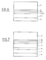
- FIGS. 6 and 7 schematically representing respectively a section of a Hall effect sensor according to this embodiment and the energy states of the corresponding conduction band.
- the references identical to those of the preceding figures designate the same type of layer.
- the layers are deposited on a substrate 10 made of a material chosen from GaAs, InP, Si in a similar manner to the previous examples.
- the buffer layer 11 the quantum well structure formed by the layers 14, 16, 18, the carrier supply layer 20 and the burial layer 22 produced in a similar manner to the previous examples.
- the Hall effect sensor has a symmetrical structure.
- the buffer layer 11 makes it possible to obtain a good surface condition and the adaptation of the mesh parameters between the materials of layer 10 (substrate) and the next layer 26 which is a layer d contribution of carriers identical to layer 20.
- a Hall effect sensor has a low temperature sensitivity (less than 150 ppm / ° C) over a wide temperature range from at least -50 ° C to + 120 ° C .
- the mobility ⁇ of the carriers in the quantum well is very high ( ⁇ is greater than 7000 cm2 / Vs), which for a given sensor geometry, greatly reduces the offset voltage ("offset" in English terminology) ( we can compare with a silicon device according to the prior art for which ⁇ ⁇ 1400 cm2 / VS). It is therefore understood that for an application to the metering of electrical energy or to the measurement of electrical currents, a sensor according to the invention does not require a compensation circuit, which facilitates the production of the meter and reduces its cost.
Landscapes
- Hall/Mr Elements (AREA)
- Measuring Fluid Pressure (AREA)
- Investigating Or Analyzing Materials By The Use Of Electric Means (AREA)
- Window Of Vehicle (AREA)
- Push-Button Switches (AREA)
Abstract
Description
La présente invention a pour objet un capteur à effet Hall. Elle s'applique notamment aux domaines de la mesure des courants électriques et du comptage de l'énergie électrique et plus particulièrement aux compteurs électriques.The present invention relates to a Hall effect sensor. It applies in particular to the fields of measurement of electric currents and metering of electric energy and more particularly to electric meters.
On sait qu'un capteur à effet Hall traversé par un courant (ou de manière équivalente soumis à une tension) d'alimentation et soumis à un champ magnétique perpendiculaire à la direction d'écoulement du courant délivre à ses bornes une tension dite de Hall selon une troisième direction de l'espace perpendiculaire aux directions du champ magnétique et d'écoulement du courant.It is known that a Hall effect sensor traversed by a supply current (or equivalent subject to a voltage) and subjected to a magnetic field perpendicular to the direction of flow of the current delivers at its terminals a so-called Hall voltage in a third direction of space perpendicular to the directions of the magnetic field and current flow.
La tension de Hall VH est proportionnelle au produit de l'intensité Ia du courant d'alimentation (ou de manière équivalente de l'amplitude de la tension d'alimentation Va) et de l'amplitude du champ magnétique B. Dans un capteur idéal, elle peut donc s'écrire :![]()
avec Ki = 1/(e.ns) où e est la charge de l'électron et ns est la densité surfacique de porteurs de charge et Kv = (W/L) µ où W et L sont respectivement la largeur et la longueur du capteur et µ est la mobilité des porteurs de charge. Dans un capteur à effet Hall réel présentant des inhomogénéités ou un désalignement des électrodes inhérents au procédé de fabrication, la tension de Hall s'écrit:![]()
où le paramètre f, petit devant 1, prend en compte les écarts à la situation idéale.
Pour obtenir une bonne sensibilité, une faible densité surfacique de porteurs est nécessaire.The Hall voltage V H is proportional to the product of the intensity I a of the supply current (or in an equivalent manner of the amplitude of the supply voltage V a ) and the amplitude of the magnetic field B. In an ideal sensor, it can therefore be written: ![]()
with K i = 1 / (in s ) where e is the charge of the electron and n s is the surface density of charge carriers and K v = (W / L) µ where W and L are respectively the width and the length of the sensor and µ is the mobility of the charge carriers. In a real Hall effect sensor exhibiting inhomogeneities or misalignment of the electrodes inherent in the manufacturing process, the Hall voltage is written: ![]()
where the parameter f, small in front of 1, takes into account the deviations from the ideal situation.
To obtain good sensitivity, a low surface density of carriers is necessary.
Ceci peut se faire par exemple en utilisant une structure semiconductrice comportant une couche conductrice homogène, d'épaisseur faible (de l'ordre du micromètre). Cette couche peut-être par exemple une couche de silicium dopée de type n sur un substrat de type P, ou bien une couche de GaAs dopée de type n sur un substrat de GaAs semi-isolant.
Ceci peut également se faire en utilisant une hétérostructure semiconductrice comportant au moins deux couches superposées de matériaux semi-conducteurs ayant une largeur de bande interdite différente, et sélectivement dopée dans le matériau de bande interdite la plus large.
Dans ce cas, les porteurs sont confinés dans une zone très fine (d'épaisseur pouvant aller de 10 à 100 angstroems) située à l'interface des deux matériaux, du côté du matériau présentant la bande interdite la moins grande.
Le capteur selon l'invention est de ce second type.This can be done for example by using a semiconductor structure comprising a homogeneous conductive layer, of small thickness (of the order of a micrometer). This layer may for example be an n-type doped silicon layer on a substrate P type, or an n type doped GaAs layer on a semi-insulating GaAs substrate.
This can also be done using a semiconductor heterostructure comprising at least two superimposed layers of semiconductor materials having a different band gap, and selectively doped in the widest band material.
In this case, the carriers are confined in a very thin zone (of thickness which can range from 10 to 100 angstroms) situated at the interface of the two materials, on the side of the material having the smallest forbidden band.
The sensor according to the invention is of this second type.
Le document US 4,912,451 décrit une hétérostructure comportant au moins deux puits quantiques : un premier puits quantique formé à l'interface entre deux couches semi-conductrices des largeurs de bande interdite différentes, et dans lequel se trouve le gaz d'électrons bidimensionnel et un second puits quantique dont la "sous-bande" dans son état fondamental présente un niveau d'énergie plus élevé que celui du gaz d'électrons bidimensionnel.Document US Pat. No. 4,912,451 describes a heterostructure comprising at least two quantum wells: a first quantum well formed at the interface between two semiconductor layers of different band gap widths, and in which the two-dimensional electron gas is found and a second quantum well whose "sub-band" in its ground state has a higher energy level than that of the two-dimensional electron gas.
Cette hétérostructure en tant que capteur à effet Hall possède une sensibilité élevée. Elle ne se sature pas, même sous l'effet d'un fort champ électrique et fournit un fort signal de sortie même dans ce cas. Par contre, cette hétérostructure est sensible aux variations de température qui influent sur le signal de sortie. Ce capteur à effet Hall doit être connecté à un dispositif électronique sophistiqué et coûteux pour permettre de compenser la dérive du signal de sortie lorsque la température varie.This heterostructure as a Hall effect sensor has a high sensitivity. It does not saturate, even under the effect of a strong electric field and provides a strong output signal even in this case. On the other hand, this heterostructure is sensitive to temperature variations which influence the output signal. This Hall effect sensor must be connected to a sophisticated and expensive electronic device to compensate for the drift of the output signal when the temperature varies.
L'article intitulé "AlGaAs:GaAs heterojunction Hall device" de T. Taguchi et publié dans Electronics and Communication in Japan, Part 2, Vol. 71, N° 3, 1988 p. 110-115 décrit une hétérojonction simple AlGaAs/GaAs utilisée comme capteur de champ magnétique. Comme précédemment, cette structure, si elle possède une sensibilité accrue ne présente pas de bonnes caractéristiques thermiques. Fabriquée pour fonctionner à température ambiante, elle nécessite un dispositif électronique de compensation si la température présente des variations. A titre indicatif, le coefficient de sensibilité à la température annoncé dans cet article est de 6800 ppm/°C.The article entitled "AlGaAs: GaAs heterojunction Hall device" by T. Taguchi and published in Electronics and Communication in Japan, Part 2, Vol. 71, No. 3, 1988 p. 110-115 describes a simple AlGaAs / GaAs heterojunction used as a magnetic field sensor. As before, this structure, if it has an increased sensitivity does not have good thermal characteristics. Manufactured to operate at room temperature, it requires an electronic compensation device if the temperature varies. As an indication, the temperature sensitivity coefficient announced in this article is 6800 ppm / ° C.
Un autre article intitulé "Highly sensitive 2DEG Hall device made of pseudomorphic InO,52AlO,48As/lnO,8GaO,2As heterostructure" rédigé par Sugiyanama et al. et publié dans "International Conférence on Solid-State Sensors and Actuators", Transducers '91, San Francisco, Digest of Technical Papers, IEEE Publications Office décrit une hétérostructure pseudomorphique InO,52AlO,48As/lnO,8GaO,2As déposée sur un substrat en InP. Bien que les performances en fonction de la température soient améliorées par rapport à celles des deux documents précédents, elles restent insuffisantes pour une application à un compteur électrique pour laquelle les spécifications exigées sont très sévères. A titre indicatif, le coefficient de sensibilité à la température d'une telle structure est de 350 ppm/°C sur un intervalle de température n'excédant pas 55°C.Another article entitled "Highly sensitive 2DEG Hall device made of pseudomorphic In O, 52 Al O, 48 As / ln O, 8 Ga O, 2 As heterostructure" written by Sugiyanama et al. and published in "International Conférence on Solid-State Sensors and Actuators", Transducers '91, San Francisco, Digest of Technical Papers, IEEE Publications Office describes a pseudomorphic heterostructure In O, 52 Al O, 48 As / ln O, 8 Ga O , 2 As deposited on an InP substrate. Although the performance as a function of temperature is improved compared to that of the two previous documents, it remains insufficient for an application to an electric meter for which the specifications required are very strict. As an indication, the temperature sensitivity coefficient of such a structure is 350 ppm / ° C over a temperature range not exceeding 55 ° C.
La présente invention a pour but de proposer un capteur à effet Hall présentant une faible sensibilité à la température (coefficient de sensibilité à la température inférieur à 150 ppm/°C) sur une gamme étendue de température (allant au moins de -50°C à + 120°C).The object of the present invention is to propose a Hall effect sensor having a low temperature sensitivity (temperature sensitivity coefficient of less than 150 ppm / ° C) over a wide temperature range (ranging from at least -50 ° C at + 120 ° C).
D'autre part, la présente invention a aussi pour but de proposer une structure à effet Hall de forte sensibilité et de faible consommation électrique.On the other hand, the present invention also aims to provide a Hall effect structure of high sensitivity and low electrical consumption.
Un autre but de l'invention est de proposer une structure à effet Hall présentant une tension de décalage ("offset" en terminologie anglosaxonne) peu importante, ou en tout cas moins important, à géométrie donnée que pour un capteur selon l'art antérieur.Another object of the invention is to propose a Hall effect structure having an offset voltage ("offset" in Anglo-Saxon terminology) which is small, or in any case less important, with a given geometry than for a sensor according to the prior art .
D'une manière générale, l'invention propose une structure minimisant, de manière notable par rapport à l'art antérieur, les corrections ou autres traitements à apporter à la mesure pour le comptage d'une énergie électrique ou la mesure d'un courant électrique.In general, the invention provides a structure which minimizes, significantly compared to the prior art, the corrections or other processing to be made to the measurement for the counting of an electrical energy or the measurement of an electric current.
De manière plus précise, la présente invention concerne un capteur semi-conducteur à effet Hall comprenant:
Une structure à puits quantique comportant une première couche d'un matériau semi-conducteur III-V, une seconde couche d'un matériau semi-conducteur III-V, et une troisième couche d'un matériau semiconducteur III-V, réalisées par épitaxie sur un substrat semiconducteur, et telle que le matériau de la seconde couche possède une bande interdite plus étroite que celle des matériaux de la première et de la troisième couche,
comportant de plus, superposée à la troisième couche, une quatrième couche de matériau semi-conducteur III-V, dite couche d'apport de porteurs, dopée par des impuretés, de type donneur n, d'épaisseur inférieure à 250 angstroems et éventuellement nulle, et dont la densité surfacique de donneurs intégrée sur toute la couche d'apport de porteurs est inférieure à 5 10¹²cm⁻², et comportant également, superposée à cette couche d'apport de porteurs une cinquième couche de matériau semi-conducteur III-V d'une épaisseur supérieure à 200 angstroems, dite couche d'enfouissement, non-dopée ou dopée par des impuretés de type accepteur, de telle sorte qu'en tout point l'énergie de la bande de conduction de cette couche soit supérieure, par exemple d'au moins 150 meV, à l'énergie de la bande de conduction dans le puits quantique.More specifically, the present invention relates to a Hall effect semiconductor sensor comprising:
A quantum well structure comprising a first layer of III-V semiconductor material, a second layer of III-V semiconductor material, and a third layer of III-V semiconductor material, produced by epitaxy on a semiconductor substrate, and such that the material of the second layer has a narrower band gap than that of the materials of the first and third layers,
further comprising, superimposed on the third layer, a fourth layer of III-V semiconductor material, called carrier supply layer, doped with impurities, of donor type n, of thickness less than 250 angstroms and possibly zero , and whose surface density of donors integrated over the entire carrier filler layer is less than 5 10¹²cm⁻², and also comprising, superimposed on this carrier filler layer a fifth layer of III-V semiconductor material of a thickness greater than 200 angstroems, called burial layer, undoped or doped with impurities of the acceptor type, so that at all points the energy of the conduction band of this layer is greater, by example of at least 150 meV, at the energy of the conduction band in the quantum well.
Entre le substrat et l'ensemble de couches formant le puits quantique se trouve une couche, dite couche tampon, d'épaisseur totale de l'ordre de quelques milliers d'angstroems, et dont le rôle est d'assurer une bonne planéité et une bonne qualité cristalline des couches épitaxiées ultérieurement.Between the substrate and the set of layers forming the quantum well is a layer, called a buffer layer, of total thickness of the order of a few thousand angstroems, and whose role is to ensure good flatness and a good crystalline quality of the epitaxial layers subsequently.
Cette couche peut être de façon connue soit une couche homogène non-dopée de matériau III-V, soit être elle-même formée par un empilement tel que par exemple un superréseau AlAs/GaAs, soit une combinaison quelconque de couches homogènes et de superréseaux.This layer can be in known manner either a homogeneous undoped layer of III-V material, or be itself formed by a stack such as, for example, an AlAs / GaAs superlattice, or any combination of homogeneous layers and superlattices.
Selon un premier mode de réalisation, la structure à puits quantique présente un puits asymétrique: La première couche est en matériau semi-conducteur III-V binaire ou ternaire. La deuxième couche est en matériau semi-conducteur III-V ternaire à plus faible largeur de bande interdite que la première couche, et la troisième couche est en matériau ternaire à plus forte largeur de bande interdite que la deuxième couche. La couche dite d'apport de porteurs étant une couche de matériau ternaire dopé, et la couche d'enfouissement une couche de matériau ternaire à grande largeur de bande interdite ou une couche de matériau ternaire à gradient de composition.According to a first embodiment, the quantum well structure has an asymmetric well: The first layer is made of binary or ternary III-V semiconductor material. The second layer is made of ternary III-V semiconductor material with a smaller band gap than the first layer, and the third layer is of ternary material with a larger band gap than the second layer. The so-called carrier supply layer being a layer of doped ternary material, and the burial layer a layer of ternary material with a large band gap or a layer of ternary material with a composition gradient.
Selon un autre mode de réalisation, la structure à puits quantique est symétrique, et comporte de part et d'autre de la deuxième couche en un matériau à plus faible largeur de bande interdite, des première et troisième couches sensiblement identiques en un matériau à plus grande largeur de bande interdite.According to another embodiment, the quantum well structure is symmetrical, and comprises on either side of the second layer made of a material with a smaller band gap, first and third substantially identical layers made of a material with more large bandwidth prohibited.
Dans ce cas, en plus des couches déjà mentionnées, une autre couche d'apport de porteurs peut être prévue entre la couche-tampon et la structure à puits quantique.In this case, in addition to the layers already mentioned, another carrier supply layer may be provided between the buffer layer and the quantum well structure.
L'invention sera mieux comprise à la lecture de la description qui suit, donnée à titre explicatif et non limitatif en référence aux dessins annexés sur lesquels:
- la figure 1 représente schématiquement une coupe d'un capteur à effet Hall selon l'invention;
- la figure 2 représente schématiquement un diagramme d'énergie de la bande de conduction d'un capteur à effet Hall conforme à l'invention;
- la figure 3 représente schématiquement une coupe d'une variante de réalisation d'un capteur à effet Hall selon l'invention;
- la figure 4 représente schématiquement une coupe d'une autre variante de réalisation d'un capteur à effet Hall selon l'invention;
- la figure 5 représente schématiquement une coupe d'une autre variante de réalisation d'un capteur à effet Hall selon l'invention;
- la figure 6 représente schématiquement une coupe d'une autre variante de réalisation d'un capteur selon l'invention.
- la figure 7 représente schématiquement une coupe d'un second mode de réalisation d'un capteur à effet Hall conforme à l'invention;
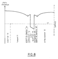
- la figure 8 représente schématiquement un diagramme de la bande de conduction d'un capteur conforme au second mode de réalisation.
- Figure 1 schematically shows a section of a Hall effect sensor according to the invention;
- FIG. 2 schematically represents an energy diagram of the conduction band of a Hall effect sensor according to the invention;
- FIG. 3 schematically represents a section of an alternative embodiment of a Hall effect sensor according to the invention;
- FIG. 4 schematically represents a section of another alternative embodiment of a Hall effect sensor according to the invention;
- FIG. 5 schematically represents a section of another alternative embodiment of a Hall effect sensor according to the invention;
- FIG. 6 schematically represents a section of another alternative embodiment of a sensor according to the invention.
- FIG. 7 schematically represents a section of a second embodiment of a Hall effect sensor according to the invention;
- FIG. 8 schematically represents a diagram of the conduction band of a sensor according to the second embodiment.
Un capteur à effet Hall conforme à l'invention comprend un empilement de couches déposées sur un substrat par toute technique connue telle l'épitaxie par jets moléculaires (Molecular Beam Epitaxy en terminologie anglosaxonne) ou l'épitaxie par déposition de vapeur chimique métalloorganique (Metallorganic Chemical Vapor Deposition en terminologie anglosaxonne).A Hall effect sensor according to the invention comprises a stack of layers deposited on a substrate by any known technique such as molecular beam epitaxy (Molecular Beam Epitaxy in English terminology) or epitaxy by deposition of metalloorganic chemical vapor (Metallorganic Chemical Vapor Deposition in English terminology).
L'homogénéité des couches ainsi que l'uniformité des dopages obtenues par ces techniques sont excellentes, cela permet de diminuer l'offset du capteur à effet Hall lié à ces paramètres.The homogeneity of the layers as well as the uniformity of the dopings obtained by these techniques are excellent, this makes it possible to reduce the offset of the Hall effect sensor linked to these parameters.
De cette manière, les opérations de calibration sont simplifiées et le coût des circuits électroniques de compensation sont réduits.In this way, the calibration operations are simplified and the cost of the electronic compensation circuits are reduced.
Selon un premier mode de réalisation, représenté schématiquement en coupe sur la figure 1, le capteur comprend un substrat 10 en matériau semi-conducteur sur lequel repose une couche tampon 11, sur laquelle se trouve une structure à puits quantique 12.
La couche tampon 11 possède une épaisseur suffisante (au moins égale à 1000 angstroems) pour obtenir une bonne qualité cristalline et une bonne planéité de surface.
La structure 12 est composée d'une première couche dite de confinement 14 en un matériau semiconducteur III-V et déposée sur le substrat, d'une deuxième couche intermédiaire 16 en un matériau semi-conducteur III-V déposée sur la première couche de confinement, d'une troisième couche 18 en un matériau semiconducteur III-V qui est une seconde couche de confinement déposée sur la couche intermédiaire. Un gaz d'électrons bidimensionnel se forme dans le puits quantique.According to a first embodiment, shown diagrammatically in section in FIG. 1, the sensor comprises a
The
The
Les couches de confinement 14, 18 présentent une forte discontinuité de bande de conduction avec la couche semi-conductrice intermédiaire 16 de manière à constituer un puits quantique le plus profond possible au niveau de la couche 16 d'affinité électronique la plus importante.The
Une couche 20 dite d'apport de porteurs en matériau semi-conducteur dopé avec un dopant de type n permettant la formation du gaz d'électrons bidimensionnel dans le puits quantique est déposée sur la structure à puits quantique 12. La seconde couche de confinement 18 permet d'éloigner les porteurs formant le gaz bidimensionnel de la zone dopée, ce qui augmente la mobilité des porteurs.
L'augmentation de la mobilité des porteurs diminue la tension de décalage ("offset" en terminologie anglosaxonne) sur la tension de Hall mesurée sur le dispositif pour un courant de polarisation Ia donné.A
The increase in the mobility of the carriers decreases the offset voltage ("offset" in English terminology) on the Hall voltage measured on the device for a given bias current I has .
L'épaisseur de la couche d'apport de porteurs 20 est inférieure à quelques centaines d'angstroems. Elle peut être nominalement nulle, le dopant étant déposé dans l'épaisseur d'un plan atomique d'une couche adjacente selon la technique connue sous le nom de dopage delta.The thickness of the
Le taux de dopage et l'épaisseur sont choisis de telle sorte que la densité surfacique de donneurs intégrée sur toute l'épaisseur de la couche d'apport de porteurs soit comprise dans une gamme allant de 10¹¹cm⁻² à 5.10¹²cm⁻².The doping rate and the thickness are chosen so that the surface density of donors integrated over the entire thickness of the carrier supply layer is in a range from 10¹¹cm⁻² to 5.10¹²cm⁻².
Le nombre de porteurs dans le puits quantique dépend d'une manière connue de la densité surfacique de donneurs intégrée sur toute l'épaisseur de la couche d'apport de porteurs ainsi que des épaisseurs et compositions des différentes couches. Cette densité surfacique de donneurs est par exemple choisie de manière à obtenir une densité surfacique de porteurs dans le puits quantique limitée à quelques 10¹¹cm⁻².
Le coefficient de Hall (équation (I)) est inversement proportionnel à la densité surfacique de porteurs. En limitant cette densité surfacique, on augmente la sensibilité, ce qui permet d'abaisser la puissance de la source d'alimentation nécessaire au fonctionnement du capteur, pour une même tension de Hall délivrée.The number of carriers in the quantum well depends in a known manner on the surface density of donors integrated over the entire thickness of the carrier supply layer as well as the thicknesses and compositions of the different layers. This surface density of donors is for example chosen so as to obtain a surface density of carriers in the quantum well limited to a few 10¹¹cm⁻².
The Hall coefficient (equation (I)) is inversely proportional to the surface density of carriers. By limiting this surface density, the sensitivity is increased, which makes it possible to lower the power of the power source necessary for the operation of the sensor, for the same Hall voltage delivered.
Une couche 22 dite d'enfouissement est déposée sur la couche d'apport de porteurs 20; cette dernière couche 22 en matériau à grande largeur de bande interdite forme une zone de charge d'espace dépeuplée de porteurs et donc électriquement isolante. De plus, I'épaisseur de cette couche est choisie dans une gamme allant d'environ 200 angstroems à quelques micromètres.A so-called
Or, toute chose étant égale par ailleurs, la dérive thermique de la densité de porteurs (et donc du signal délivré par le capteur) est d'autant plus faible que l'épaisseur d'une telle couche d'enfouissement est importante. L'épaisseur de la couche n'est limitée que par l'apparition de dislocations ou autres défauts.However, all other things being equal, the thermal drift of the carrier density (and therefore of the signal delivered by the sensor) is all the smaller the greater the thickness of such a burial layer. The thickness of the layer is only limited by the appearance of dislocations or other defects.
Avantageusement, I'énergie de la bande de conduction de la couche d'enfouissement 22 est en tout point supérieure d'au moins 150 meV à l'énergie de la bande de conduction dans le puits quantique. De cette manière, le nombre de porteurs présents dans la couche d'enfouissement 22 est négligeable devant le nombre de porteurs dans le puits quantique 16, et ne perturbe donc pas la mesure d'effet Hall.Advantageously, the energy of the conduction band of the
Après l'achèvement du dépôt des différentes couches décrites ci-dessus, on fabrique un motif de Hall possédant au moins 4 contacts. Le motif de Hall peut être réalisé par gravure sèche ou humide de l'ensemble des couches 11 à 22; des contacts conducteurs sont ensuite formés sur le motif.
On peut également délimiter des zones conductrices en utilisant une technique d'implantation, de manière à rendre non-conducteurs l'ensemble des couches en dehors du motif de Hall. Les contacts ohmiques sont alors réalisés par métallisation pour l'alimentation du dispositif et la mesure de la tension de Hall.
Le dispositif peut être passivé par dépôt d'une couche diélectrique appropriée telle que par exemple SiO₂ ou Si₃N₄.After the completion of the deposition of the various layers described above, a Hall pattern is produced having at least 4 contacts. The Hall pattern can be produced by dry or wet etching of all of the
It is also possible to delimit conductive zones using an implantation technique, so as to make all of the layers outside the Hall pattern non-conductive. The ohmic contacts are then produced by metallization to supply the device and measure the Hall voltage.
The device can be passivated by deposition of an appropriate dielectric layer such as for example SiO₂ or Si₃N₄.
La figure 2 représente schématiquement un diagramme d'énergie de la bande de conduction d'un capteur à effet Hall selon le premier mode de réalisation.FIG. 2 schematically represents an energy diagram of the conduction band of a Hall effect sensor according to the first embodiment.
La structure à puits quantique 12 à forte discontinuité de bande, telle qu'elle est réalisée par les couches 14, 16, 18 permet d'obtenir un puits profond dans lequel le gaz d'électrons bidimensionnel est bien confiné.The
Les atomes dopants de la couche d'apport de porteurs 20 possèdent des états d'énergie non représentés, résonants ou localisés dans la bande interdite, au voisinage de la bande de conduction de la couche. Dans la configuration de l'invention, ces états localisés présentent une énergie supérieure d'au moins 300 meV à celle des électrons du gaz d'électrons bidimensionnel. De cette manière, on évite le phénomène dit de gel des porteurs qui correspond à une non ionisation des atomes dopants. Or la proportion de porteurs gelés sur ces états localisés varie en fonction de la température. Empêcher l'apparition de ce phénomène permet donc d'éviter une source de dérive du signal de Hall avec la température.The doping atoms of the
Le premier mode de réalisation se rapportant aux figures 1 et 2 va être décrit avec plus de détails dans les exemples suivants cités à titre indicatif et non limitatif.The first embodiment relating to FIGS. 1 and 2 will be described in more detail in the following examples, which are given for information only and are not limiting.
Le substrat 10 est en GaAs; la couche de tampon 11 peut être alors choisie parmi une couche de GaAs, une couche formée par un superréseau AlAs/GaAs ou encore une couche formée par la superposition de GaAs déposée sur le substrat et d'une couche formée par un superréseau AlAs/GaAs.The
La première couche de confinement 14 peut être une couche de GaAs non dopé. En variante, cette couche peut être éventuellement confondue avec la couche tampon 11 qui remplit alors les deux fonctions de tampon et de confinement. Son épaisseur est comprise entre 0 et quelques milliers d'angstroems.The
La couche semi-conductrice intermédiaire 16 est en InxGa1-xAs non dopé, avec une composition x comprise dans une gamme allant de 0 à 1, préférentiellement allant de 0 à 0,4 et par exemple égale à 0,15. Son épaisseur est comprise dans une gamme allant de 10 angstroems à 500 angstroems, par exemple 130 A.The
La troisième couche 18 dite de confinement est en AlyGa1-yAs non dopé de composition y compris dans une gamme allant de 0 à 0,4; y peut être par exemple égale à 0,32. L'épaisseur de la couche 18 est inférieure à 200 angstroems. Elle peut être par exemple de 40 Ä.The third so-called
En variante, la troisième couche 18 de confinement est formée par un superréseau à courte période AlAs/GaAs, par exemple du type n/m, n représentant le nombre de couches atomiques d'AlAs et m représentant le nombre de couches atomiques de GaAs. Si n et m sont assez petits, par exemple compris entre 1 et 10, ce superréseau AlAs/GaAs n/m a des propriétés électriques très proches de celles de l'alliage désordonné AlyGa1-yAs, avec y=n/(n+m), et est appelé pseudoalliage.As a variant, the
Dans un cas extrême, représenté schématiquement en coupe sur la figure 3, cette couche de confinement peut être omise, son épaisseur étant nulle. La couche d'apport de porteurs 20 repose alors directement sur la couche semi-conductrice intermédiaire 16.In an extreme case, shown diagrammatically in section in FIG. 3, this confinement layer can be omitted, its thickness being zero. The
La couche d'apport de porteurs 20 est en AluGa1-uAs dopé avec un dopant de type n choisi parmi les éléments des colonnes IV (par exemple Si, Ge, Sn) ou VI (par exemple S, Se, Te) du tableau périodique. Avantageusement, lorsqu'on utilise la technique d'épitaxie par jets moléculaires, on choisit le silicium comme dopant.The
Le taux de dopage est choisi de sorte que la densité surfacique d'atomes dopants intégrée sur toute l'épaisseur de la couche d'apport de porteurs soit comprise entre 10¹¹cm⁻² et 10¹²cm⁻². La densité surfacique de donneurs peut être par exemple de 10¹²cm⁻².The doping rate is chosen so that the surface density of doping atoms integrated over the entire thickness of the carrier supply layer is between 10¹¹cm⁻² and 10¹²cm⁻². The surface density of donors can be for example 10¹²cm⁻².
La composition u est comprise dans une gamme allant de 0 à 0,4; elle peut être par exemple de 0,32.The composition u is in a range from 0 to 0.4; it can for example be 0.32.
L'épaisseur de la couche d'apport de porteurs est inférieure à quelques centaines d'angstroems ; elle peut être par exemple de 40 Ä.The thickness of the carrier filler layer is less than a few hundred angstroms; it can for example be 40 Ä.
Selon une variante de réalisation représentée schématiquement en coupe sur la figure 4, la couche 20 est d'épaisseur nominalement nulle ; le dopant, formant seul la couche, est représenté en pointillés. Le dépôt du dopant est effectué dans l'épaisseur d'un plan atomique de la seconde couche de confinement 18 selon la technique connue sous le nom de "dopage delta".According to an alternative embodiment shown diagrammatically in section in FIG. 4, the
L'utilisation d'une couche de porteurs d'épaisseur très faible, et plus encore l'utilisation du dopage delta, permet de minimiser le piégeage des porteurs sur les états localisés des atomes dopants, et par conséquence d'obtenir une faible dérive thermique du coefficient de Hall.The use of a very thin layer of carriers, and even more the use of delta doping, makes it possible to minimize the trapping carriers on the localized states of the doping atoms, and consequently to obtain a weak thermal drift of the Hall coefficient.
Selon une variante de réalisation, la couche d'apport de porteurs 20 est réalisée par un superréseau à courte période en AlAs/GaAs formant un pseudo-alliage (le superréseau peut être du type n/2n avec n représentant le nombre de couches atomiques et n étant compris entre 1 et 10).According to an alternative embodiment, the
La couche d'enfouissement 22 est en AlqGa1-qAs non dopé de composition q comprise dans une gamme allant de 0 à 0,4 et par exemple égale à 0,32.The
L'épaisseur de la couche d'enfouissement 22 est comprise dans une gamme allant de 200 angstroems à 2 microns; elle peut être par exemple de 3000 Ä.The thickness of the
Selon une variante de réalisation représentée schématiquement en coupe sur la figure 5, pour éviter tout dopage résiduel de type p pouvant survenir dans une couche trop épaisse, la couche d'enfouissement 22 est formée par une première couche 22a en AlpGa1-pAs ayant une composition p comprise dans une gamme allant de O à 0,4 et par exemple égale à 0,32.According to an alternative embodiment shown diagrammatically in section in FIG. 5, to avoid any p-type residual doping which may occur in a layer that is too thick, the
L'épaisseur de cette première couche 22a est comprise dans une gamme allant de 200 angströms à quelques milliers d'angstroems; elle peut être par exemple de 500 Ä.The thickness of this
Une seconde couche 22b en AlwGa1-wAs possédant un gradient de composition, c'est à dire que w varie de la composition de la couche précédente 22a à 0. De cette manière, la transition est assurée vers une couche de GaAs dont le dopage résiduel est beaucoup mieux contrôlé lors d'un dépôt par épitaxie par jets moléculaires ou par MOCVD.A
L'épaisseur de la couche 22b est comprise dans une gamme allant de 0 à 2 micromètres et est par exemple égale à 2500 angstroems.The thickness of the
La couche 22 d'enfouissement peut aussi être formée par un superréseau à courte période AlAs/GaAs (du même type que les superréseaux précédemment cités) formant un pseudo alliage.The
Dans cet exemple, le substrat est en silicium. La première couche de confinement 14 jouant le rôle de tampon est par exemple, un superréseau AlAs/GaAs qui assure la relaxation des contraintes dues à la différence de paramètres de maille des cristaux de Si d'une part et de GaAs ou AlAs d'autre part.
D'une manière générale, le superréseau peut être du type AlzGa1-zAs/GaAs avec la composition z comprise dans une gamme allant de 0 à 1.Le reste de la structure peut être identique à ce qui a été décrit pour l'EXEMPLE 1.In this example, the substrate is made of silicon. The
In general, the superlattice can be of the Al z Ga 1-z As / GaAs type with the composition z in a range from 0 to 1. The rest of the structure can be identical to what has been described for EXAMPLE 1.
Le substrat est en InP. La couche tampon 11 est par exemple une couche d' InP. Son épaisseur peut prendre les mêmes valeurs que la couche tampon 11 de l'EXEMPLE 1. La couche tampon 11 est en InGaAs.
Dans une variante de réalisation, la couche tampon 11 peut aussi être un superréseau du type InGaAs/lnAlAs ou encore être composé d'une couche InP recouverte par un superréseau du type InGaAs/lnAlAs.The substrate is made of InP. The
In an alternative embodiment, the
La première couche de confinement 14 est une couche d'lnP non dopée. La couche semiconductrice intermédiaire 16 est en InxGa1-xAs adaptée en paramètre de maille avec InP, c'est à dire avec une composition x comprise dans une gamme allant de 0,5 à 0,56 et par exemple voisine de 0,53. La seconde couche de confinement 18 est une couche d'InyAl1-yAs également adaptée en paramètre de maille avec InP, c'est à dire avec une composition y comprise dans une gamme allant de 0,5 à 0,56 et par exemple voisine de 0,52.The
La couche d'apport de porteurs 20 et la couche d'enfouissement 22 sont en IniAl1-iAs avec une composition i comprise dans une gamme allant de 0,5 à 0,56 par exemple 0,52.
Les épaisseurs de chacune de ces couches sont du même ordre que celles de l'EXEMPLE 1; ainsi, dans une variante, la couche d'apport de porteurs 20 peut être d'épaisseur nominalement nulle par "dopage delta".The
The thicknesses of each of these layers are of the same order as those of EXAMPLE 1; thus, in a variant, the
On décrit maintenant un second mode de réalisation en référence aux figures 6 et 7 représentant de manière schématique respectivement une coupe d'un capteur à effet Hall selon ce mode de réalisation et les états d'énergie de la bande de conduction correspondante.
Les références identiques à celles des figures précédentes désignent le même type de couche.
Ainsi, les couches sont déposées sur un substrat 10 en un matérieu choisi parmi GaAs, InP, Si de manière similaire aux exemples précédents. On retrouve dans ce mode de réalisation la couche tampon 11, la structure à puits quantique formée par les couches 14, 16,18, la couche d'apport de porteurs 20 et la couche d'enfouissement 22 réalisées de manière similaire aux exemples précédents.
Comme on peut le voir sur les figures 6 et 7, le capteur à effet Hall possède une structure symétrique. La couche tampon 11, de même que dans les exemples précédents, permet d'obtenir un bon état de surface et l'adaptation des paramètres de maille entre les matériaux de la couche 10 (substrat) et la couche suivante 26 qui est une couche d'apport de porteurs identique à la couche 20.A second embodiment will now be described with reference to FIGS. 6 and 7 schematically representing respectively a section of a Hall effect sensor according to this embodiment and the energy states of the corresponding conduction band.
The references identical to those of the preceding figures designate the same type of layer.
Thus, the layers are deposited on a
As can be seen in Figures 6 and 7, the Hall effect sensor has a symmetrical structure. The
Grâce à sa structure particulière, un capteur à effet Hall conforme à l'invention possède une faible sensibilité en température (inférieure à 150 ppm/°C) sur une gamme étendue de température allant au moins de -50°C à + 120°C. De plus, la mobilité µ des porteurs dans le puits quantique est très élevée (µ est supérieure à 7000 cm²/V.s), ce qui pour une géométrie de capteur donnée, diminue fortement la tension de décalage ("offset" en terminologie anglosaxonne) (on peut comparer avec un dispositif en silicium conforme à l'art antérieur pour lequel µ ≦1400 cm²/V.S). On comprend donc que pour une application au comptage de l'énergie électrique ou à la mesure de courants électriques, un capteur selon l'invention ne nécessite pas de circuit de compensation ce qui facilite la réalisation du compteur et diminue son coût.Thanks to its particular structure, a Hall effect sensor according to the invention has a low temperature sensitivity (less than 150 ppm / ° C) over a wide temperature range from at least -50 ° C to + 120 ° C . In addition, the mobility µ of the carriers in the quantum well is very high (µ is greater than 7000 cm² / Vs), which for a given sensor geometry, greatly reduces the offset voltage ("offset" in English terminology) ( we can compare with a silicon device according to the prior art for which µ ≦ 1400 cm² / VS). It is therefore understood that for an application to the metering of electrical energy or to the measurement of electrical currents, a sensor according to the invention does not require a compensation circuit, which facilitates the production of the meter and reduces its cost.
Claims (19)
une première couche (14) en matériau semiconducteur III-V, une deuxième couche (16) en matériau semiconducteur III-V ayant une bande interdite de plus faible largeur que la bande interdite de la première couche (14), une troisième couche (18) en matériau semiconducteur III-V ayant une bande interdite de plus grande largeur que la bande interdite de la première couche (14).Sensor according to claim 1, characterized in that the quantum well structure (12) comprises:
a first layer (14) of III-V semiconductor material, a second layer (16) of III-V semiconductor material having a band gap of narrower width than the band of the first layer (14), a third layer (18 ) in III-V semiconductor material having a forbidden band of greater width than the forbidden band of the first layer (14).
Applications Claiming Priority (2)
| Application Number | Priority Date | Filing Date | Title |
|---|---|---|---|
| FR929206517A FR2691839B1 (en) | 1992-05-27 | 1992-05-27 | HALL EFFECT SENSOR. |
| FR9206517 | 1992-05-27 |
Publications (2)
| Publication Number | Publication Date |
|---|---|
| EP0572298A1 true EP0572298A1 (en) | 1993-12-01 |
| EP0572298B1 EP0572298B1 (en) | 1996-09-25 |
Family
ID=9430250
Family Applications (1)
| Application Number | Title | Priority Date | Filing Date |
|---|---|---|---|
| EP93401267A Expired - Lifetime EP0572298B1 (en) | 1992-05-27 | 1993-05-18 | Hall effect sensor |
Country Status (7)
| Country | Link |
|---|---|
| US (1) | US5442221A (en) |
| EP (1) | EP0572298B1 (en) |
| AT (1) | ATE143531T1 (en) |
| CA (1) | CA2095964C (en) |
| DE (1) | DE69304995T2 (en) |
| ES (1) | ES2092247T3 (en) |
| FR (1) | FR2691839B1 (en) |
Cited By (1)
| Publication number | Priority date | Publication date | Assignee | Title |
|---|---|---|---|---|
| FR2768263A1 (en) * | 1997-09-09 | 1999-03-12 | Thomson Csf | HALL EFFECT SENSOR |
Families Citing this family (23)
| Publication number | Priority date | Publication date | Assignee | Title |
|---|---|---|---|---|
| US5883564A (en) * | 1994-04-18 | 1999-03-16 | General Motors Corporation | Magnetic field sensor having high mobility thin indium antimonide active layer on thin aluminum indium antimonide buffer layer |
| US6266623B1 (en) | 1994-11-21 | 2001-07-24 | Phatrat Technology, Inc. | Sport monitoring apparatus for determining loft time, speed, power absorbed and other factors such as height |
| US8280682B2 (en) | 2000-12-15 | 2012-10-02 | Tvipr, Llc | Device for monitoring movement of shipped goods |
| US7386401B2 (en) | 1994-11-21 | 2008-06-10 | Phatrat Technology, Llc | Helmet that reports impact information, and associated methods |
| FR2749695B1 (en) * | 1996-06-06 | 1998-07-24 | Silmag Sa | MAGNETIC WRITING AND READING HEAD WITH SEMICONDUCTOR FIELD DETECTOR |
| US5831513A (en) * | 1997-02-04 | 1998-11-03 | United Microelectronics Corp. | Magnetic field sensing device |
| US6208154B1 (en) | 1998-08-10 | 2001-03-27 | Advanced Micro Devices, Inc. | Method of determining the doping concentration across a surface of a semiconductor material |
| US6147507A (en) * | 1998-08-10 | 2000-11-14 | Advanced Micro Devices, Inc. | System and method of mapping leakage current and a defect profile of a semiconductor dielectric layer |
| US6320403B1 (en) | 1998-08-10 | 2001-11-20 | Advanced Micro Devices, Inc. | Method of determining the doping concentration and defect profile across a surface of a processed semiconductor material |
| US7171331B2 (en) | 2001-12-17 | 2007-01-30 | Phatrat Technology, Llc | Shoes employing monitoring devices, and associated methods |
| US20040061493A1 (en) * | 2001-09-25 | 2004-04-01 | Keith Fishburn | Tone wheel |
| US6642709B2 (en) | 2001-10-17 | 2003-11-04 | A.J. Rose Manufacturing Co. | Signal wheel for generating rotational position signal |
| US7847536B2 (en) * | 2006-08-31 | 2010-12-07 | Itron, Inc. | Hall sensor with temperature drift control |
| US9081041B2 (en) * | 2012-04-04 | 2015-07-14 | Allegro Microsystems, Llc | High accuracy differential current sensor for applications like ground fault interrupters |
| US8896295B2 (en) | 2012-04-04 | 2014-11-25 | Allegro Microsystems, Llc | Magnetic field sensor having multiple sensing elements and a programmable misalignment adjustment device for misalignment detection and correction in current sensing and other applications |
| US9007054B2 (en) | 2012-04-04 | 2015-04-14 | Allegro Microsystems, Llc | Angle sensor with misalignment detection and correction |
| US9640389B2 (en) | 2014-06-17 | 2017-05-02 | Brolis Semiconductors Ltd. | High-mobility semiconductor heterostructures |
| EP3629927A1 (en) | 2017-05-22 | 2020-04-08 | UAB Brolis Semiconductors | Tunable hybrid iii-v/ iv laser sensor system-on-a-chip for real-time monitoring of a blood constituent concentration level |
| DE102017217285A1 (en) * | 2017-09-28 | 2019-03-28 | Robert Bosch Gmbh | Layer composite for the electrostatic doping of a two-dimensional doping layer, Hall sensor and method and apparatus for producing such a layer composite |
| EP3747092A1 (en) | 2018-02-02 | 2020-12-09 | Brolis Sensor Technology, UAB | Wavelength determination for widely tunable lasers and laser systems thereof |
| US11605778B2 (en) | 2019-02-07 | 2023-03-14 | Lake Shore Cryotronics, Inc. | Hall effect sensor with low offset and high level of stability |
| KR20210098725A (en) * | 2020-02-03 | 2021-08-11 | 삼성전자주식회사 | Infrared detecting device and infrared detecting system including the same |
| EP3866215A1 (en) * | 2020-02-14 | 2021-08-18 | Melexis Technologies SA | Semiconductor stack for hall effect device |
Citations (1)
| Publication number | Priority date | Publication date | Assignee | Title |
|---|---|---|---|---|
| US4912451A (en) * | 1988-03-28 | 1990-03-27 | Nippon Soken, Inc. | Heterojunction magnetic field sensor |
Family Cites Families (10)
| Publication number | Priority date | Publication date | Assignee | Title |
|---|---|---|---|---|
| JPH06105802B2 (en) * | 1984-07-09 | 1994-12-21 | 旭化成工業株式会社 | Magnetoelectric conversion element |
| US4882609A (en) * | 1984-11-19 | 1989-11-21 | Max-Planck Gesellschaft Zur Forderung Der Wissenschafter E.V. | Semiconductor devices with at least one monoatomic layer of doping atoms |
| DE3676019D1 (en) * | 1985-09-03 | 1991-01-17 | Daido Steel Co Ltd | EPITACTIC GALLIUM ARSENIDE SEMICONDUCTOR DISC AND METHOD FOR THEIR PRODUCTION. |
| JPS6293989A (en) * | 1985-10-21 | 1987-04-30 | Hitachi Ltd | Hall element |
| JP2557373B2 (en) * | 1986-04-05 | 1996-11-27 | 住友電気工業株式会社 | Compound semiconductor device |
| JPS6354785A (en) * | 1986-08-25 | 1988-03-09 | Agency Of Ind Science & Technol | Hetero-junction magnetic sensor |
| EP0314836A1 (en) * | 1987-11-06 | 1989-05-10 | Max-Planck-Gesellschaft zur Förderung der Wissenschaften e.V. | Semiconductor device in particular a hot electron transistor |
| JPH01125003A (en) * | 1987-06-24 | 1989-05-17 | Yagi Antenna Co Ltd | Reflector for yagi antenna |
| JP2553731B2 (en) * | 1990-04-13 | 1996-11-13 | 三菱電機株式会社 | Semiconductor optical device |
| FR2679071B1 (en) * | 1991-07-08 | 1997-04-11 | France Telecom | FIELD EFFECT TRANSISTOR WITH THIN FILMS OF CONTROLLED ENERGY STRIP. |
-
1992
- 1992-05-27 FR FR929206517A patent/FR2691839B1/en not_active Expired - Fee Related
-
1993
- 1993-05-11 CA CA002095964A patent/CA2095964C/en not_active Expired - Fee Related
- 1993-05-18 DE DE69304995T patent/DE69304995T2/en not_active Expired - Fee Related
- 1993-05-18 AT AT93401267T patent/ATE143531T1/en not_active IP Right Cessation
- 1993-05-18 EP EP93401267A patent/EP0572298B1/en not_active Expired - Lifetime
- 1993-05-18 ES ES93401267T patent/ES2092247T3/en not_active Expired - Lifetime
- 1993-05-24 US US08/065,003 patent/US5442221A/en not_active Expired - Lifetime
Patent Citations (1)
| Publication number | Priority date | Publication date | Assignee | Title |
|---|---|---|---|---|
| US4912451A (en) * | 1988-03-28 | 1990-03-27 | Nippon Soken, Inc. | Heterojunction magnetic field sensor |
Non-Patent Citations (2)
| Title |
|---|
| PATENT ABSTRACTS OF JAPAN vol. 11, no. 294 (E-544)22 Septembre 1987 & JP-A-62 093 989 ( HITACHI LTD ) 30 Avril 1987 * |
| PATENT ABSTRACTS OF JAPAN vol. 12, no. 273 (E-639)29 Juillet 1988 & JP-A-63 054 785 ( AGENCY OF IND. SCIENCE & TECHNOL. ) 9 Mars 1988 * |
Cited By (2)
| Publication number | Priority date | Publication date | Assignee | Title |
|---|---|---|---|---|
| FR2768263A1 (en) * | 1997-09-09 | 1999-03-12 | Thomson Csf | HALL EFFECT SENSOR |
| EP0902489A1 (en) * | 1997-09-09 | 1999-03-17 | Thomson Csf | Hall effect sensor |
Also Published As
| Publication number | Publication date |
|---|---|
| DE69304995D1 (en) | 1996-10-31 |
| DE69304995T2 (en) | 1997-02-06 |
| CA2095964A1 (en) | 1993-11-28 |
| FR2691839A1 (en) | 1993-12-03 |
| ATE143531T1 (en) | 1996-10-15 |
| FR2691839B1 (en) | 1994-08-05 |
| EP0572298B1 (en) | 1996-09-25 |
| CA2095964C (en) | 2003-10-14 |
| ES2092247T3 (en) | 1996-11-16 |
| US5442221A (en) | 1995-08-15 |
Similar Documents
| Publication | Publication Date | Title |
|---|---|---|
| EP0572298B1 (en) | Hall effect sensor | |
| EP0236189B1 (en) | Monolithic semiconductor structure of a heterojunction bipolar transistor and a laser | |
| WO2009156657A1 (en) | Field effect superconductor transistor and method for making such transistor | |
| EP0335793B1 (en) | Semiconductor pressure transducer | |
| EP1604220A1 (en) | Magnetoresistive sensor, comprising a ferromagnetic/antiferromagnetic sensitive element | |
| EP3203526A1 (en) | Heterojunction transistor with improved electron gas confinement | |
| EP0235029A1 (en) | Optical detector of the integrated optics type and its method of manufacture | |
| EP2786426B1 (en) | Semiconductor structure able to receive electromagnetic radiation, semiconductor component and process for fabricating such a semiconductor structure | |
| CA2421077C (en) | Hall-effect sensor | |
| FR3026892A1 (en) | FIELD EFFECT TRANSISTOR WITH OPTIMIZED MIXED DRAIN CONTACT AND METHOD OF MANUFACTURE | |
| EP0454544B1 (en) | Hydrostatic pressure transducer | |
| EP4194864A1 (en) | Test vehicle and test method for microelectronic devices | |
| JPH06314813A (en) | P-i-n photosensitive element, its manufacture and photoelectronic integrated circuit | |
| FR2604828A1 (en) | METHOD FOR MANUFACTURING A P + NN + DIODE AND A BIPOLAR TRANSISTOR HAVING THE SAME, USING THE NEUTRALIZATION EFFECT OF DONOR ATOMS BY ATOMIC HYDROGEN | |
| FR2666455A1 (en) | OPTOELECTRONIC DEVICE AND APPLICATION TO THE PRODUCTION OF A LASER AND A PHOTODETECTOR. | |
| FR3068512B1 (en) | TWO-DIMENSIONAL ELECTRON GAS FIELD EFFECT TRANSISTOR, COMPONENT AND RELATED METHODS | |
| FR3058831B1 (en) | HETEROJUNCTION ELECTRONIC COMPONENT HAVING HIGH ELECTRONIC MOBILITY | |
| EP0027761A1 (en) | High-frequency field effect semiconductor device and transistor using such a semiconductor device | |
| FR2690277A1 (en) | Integrated circuit with complementary heterojunction field effect transistors. | |
| JP7200651B2 (en) | Semiconductor wafer, infrared detector, imaging device using same, method for manufacturing semiconductor wafer, and method for manufacturing infrared detector | |
| Nathan et al. | Type II superlattice infrared detector and focal plane arrays | |
| EP2929535B1 (en) | Varistor | |
| FR2766919A1 (en) | Hydrostatic pressure and-or temperature transducer useful for oil well pressure sensor | |
| Monroy et al. | Visible-blind ultraviolet photodetectors based on A lx G a 1-x N alloys | |
| Kondrat et al. | Effect of modifying a Bi nanolayer on the charge transport in Sb-n-Si-Bi-Ge 33 As 12 Se 55-Sb heterostructures |
Legal Events
| Date | Code | Title | Description |
|---|---|---|---|
| PUAI | Public reference made under article 153(3) epc to a published international application that has entered the european phase |
Free format text: ORIGINAL CODE: 0009012 |
|
| AK | Designated contracting states |
Kind code of ref document: A1 Designated state(s): AT BE CH DE ES FR GB IE IT LI NL PT SE |
|
| 17P | Request for examination filed |
Effective date: 19940415 |
|
| 17Q | First examination report despatched |
Effective date: 19950522 |
|
| GRAG | Despatch of communication of intention to grant |
Free format text: ORIGINAL CODE: EPIDOS AGRA |
|
| GRAH | Despatch of communication of intention to grant a patent |
Free format text: ORIGINAL CODE: EPIDOS IGRA |
|
| GRAH | Despatch of communication of intention to grant a patent |
Free format text: ORIGINAL CODE: EPIDOS IGRA |
|
| GRAA | (expected) grant |
Free format text: ORIGINAL CODE: 0009210 |
|
| ITF | It: translation for a ep patent filed | ||
| AK | Designated contracting states |
Kind code of ref document: B1 Designated state(s): AT BE CH DE ES FR GB IE IT LI NL PT SE |
|
| REF | Corresponds to: |
Ref document number: 143531 Country of ref document: AT Date of ref document: 19961015 Kind code of ref document: T |
|
| REG | Reference to a national code |
Ref country code: CH Ref legal event code: NV Representative=s name: A. BRAUN, BRAUN, HERITIER, ESCHMANN AG PATENTANWAE |
|
| REF | Corresponds to: |
Ref document number: 69304995 Country of ref document: DE Date of ref document: 19961031 |
|
| GBT | Gb: translation of ep patent filed (gb section 77(6)(a)/1977) |
Effective date: 19961014 |
|
| REG | Reference to a national code |
Ref country code: IE Ref legal event code: FG4D Free format text: 70005 |
|
| REG | Reference to a national code |
Ref country code: ES Ref legal event code: FG2A Ref document number: 2092247 Country of ref document: ES Kind code of ref document: T3 |
|
| REG | Reference to a national code |
Ref country code: PT Ref legal event code: SC4A Free format text: AVAILABILITY OF NATIONAL TRANSLATION Effective date: 19961007 |
|
| PLBE | No opposition filed within time limit |
Free format text: ORIGINAL CODE: 0009261 |
|
| STAA | Information on the status of an ep patent application or granted ep patent |
Free format text: STATUS: NO OPPOSITION FILED WITHIN TIME LIMIT |
|
| 26N | No opposition filed | ||
| REG | Reference to a national code |
Ref country code: GB Ref legal event code: IF02 |
|
| REG | Reference to a national code |
Ref country code: FR Ref legal event code: GC |
|
| BECH | Be: change of holder |
Owner name: *SCHLUMBERGER ELECTRICITY INC. Effective date: 20040202 |
|
| REG | Reference to a national code |
Ref country code: CH Ref legal event code: PUE Owner name: SCHLUMBERGER INDUSTRIES S.A. Free format text: SCHLUMBERGER INDUSTRIES S.A.#50, AVENUE JEAN-JAURES#F-92120 MONTROUGE (FR) -TRANSFER TO- SCHLUMBERGER INDUSTRIES S.A.#313-B NORTH HIGHWAY 11#WEST UNION, SC 29696 (US) Ref country code: CH Ref legal event code: NV Representative=s name: DR. LUSUARDI AG |
|
| REG | Reference to a national code |
Ref country code: CH Ref legal event code: PUE Owner name: SCHLUMBERGER INDUSTRIES S.A. Free format text: SCHLUMBERGER INDUSTRIES S.A.#50, AVENUE JEAN-JAURES#F-92120 MONTROUGE (FR) -TRANSFER TO- SCHLUMBERGER INDUSTRIES S.A.#313-B NORTH HIGHWAY 11#WEST UNION, SC 29696 (US) Ref country code: CH Ref legal event code: PK Free format text: RECTIFICATION. Ref country code: CH Ref legal event code: NV Representative=s name: DR. LUSUARDI AG |
|
| NLS | Nl: assignments of ep-patents |
Owner name: SCHLUMBERGER ELECTRICITY, INC. |
|
| NLT1 | Nl: modifications of names registered in virtue of documents presented to the patent office pursuant to art. 16 a, paragraph 1 |
Owner name: SCHLUMBERGER S.A. |
|
| REG | Reference to a national code |
Ref country code: PT Ref legal event code: PD4A Free format text: SCHLUMBERGER SA FR Effective date: 20040311 Ref country code: PT Ref legal event code: PC4A Free format text: SCHLUMBERGER ELECTRICITY, INC. US Effective date: 20040311 |
|
| REG | Reference to a national code |
Ref country code: FR Ref legal event code: DG |
|
| REG | Reference to a national code |
Ref country code: FR Ref legal event code: TP |
|
| REG | Reference to a national code |
Ref country code: GB Ref legal event code: 732E |
|
| REG | Reference to a national code |
Ref country code: ES Ref legal event code: PC2A |
|
| PGFP | Annual fee paid to national office [announced via postgrant information from national office to epo] |
Ref country code: NL Payment date: 20090524 Year of fee payment: 17 Ref country code: IE Payment date: 20090527 Year of fee payment: 17 Ref country code: ES Payment date: 20090526 Year of fee payment: 17 |
|
| PGFP | Annual fee paid to national office [announced via postgrant information from national office to epo] |
Ref country code: SE Payment date: 20090528 Year of fee payment: 17 Ref country code: PT Payment date: 20090512 Year of fee payment: 17 Ref country code: IT Payment date: 20090528 Year of fee payment: 17 Ref country code: FR Payment date: 20090518 Year of fee payment: 17 Ref country code: DE Payment date: 20090528 Year of fee payment: 17 Ref country code: AT Payment date: 20090505 Year of fee payment: 17 |
|
| PGFP | Annual fee paid to national office [announced via postgrant information from national office to epo] |
Ref country code: BE Payment date: 20090624 Year of fee payment: 17 |
|
| PGFP | Annual fee paid to national office [announced via postgrant information from national office to epo] |
Ref country code: CH Payment date: 20090526 Year of fee payment: 17 |
|
| PGFP | Annual fee paid to national office [announced via postgrant information from national office to epo] |
Ref country code: GB Payment date: 20090528 Year of fee payment: 17 |
|
| REG | Reference to a national code |
Ref country code: PT Ref legal event code: MM4A Free format text: LAPSE DUE TO NON-PAYMENT OF FEES Effective date: 20101118 |
|
| BERE | Be: lapsed |
Owner name: *SCHLUMBERGER ELECTRICITY INC. Effective date: 20100531 |
|
| REG | Reference to a national code |
Ref country code: NL Ref legal event code: V1 Effective date: 20101201 |
|
| REG | Reference to a national code |
Ref country code: CH Ref legal event code: PL |
|
| GBPC | Gb: european patent ceased through non-payment of renewal fee |
Effective date: 20100518 |
|
| PG25 | Lapsed in a contracting state [announced via postgrant information from national office to epo] |
Ref country code: AT Free format text: LAPSE BECAUSE OF NON-PAYMENT OF DUE FEES Effective date: 20100518 |
|
| EUG | Se: european patent has lapsed | ||
| REG | Reference to a national code |
Ref country code: FR Ref legal event code: ST Effective date: 20110131 |
|
| PG25 | Lapsed in a contracting state [announced via postgrant information from national office to epo] |
Ref country code: PT Free format text: LAPSE BECAUSE OF NON-PAYMENT OF DUE FEES Effective date: 20101118 Ref country code: LI Free format text: LAPSE BECAUSE OF NON-PAYMENT OF DUE FEES Effective date: 20100531 Ref country code: CH Free format text: LAPSE BECAUSE OF NON-PAYMENT OF DUE FEES Effective date: 20100531 |
|
| REG | Reference to a national code |
Ref country code: IE Ref legal event code: MM4A |
|
| PG25 | Lapsed in a contracting state [announced via postgrant information from national office to epo] |
Ref country code: NL Free format text: LAPSE BECAUSE OF NON-PAYMENT OF DUE FEES Effective date: 20101201 Ref country code: BE Free format text: LAPSE BECAUSE OF NON-PAYMENT OF DUE FEES Effective date: 20100531 Ref country code: IT Free format text: LAPSE BECAUSE OF NON-PAYMENT OF DUE FEES Effective date: 20100518 Ref country code: SE Free format text: LAPSE BECAUSE OF NON-PAYMENT OF DUE FEES Effective date: 20100519 |
|
| PG25 | Lapsed in a contracting state [announced via postgrant information from national office to epo] |
Ref country code: DE Free format text: LAPSE BECAUSE OF NON-PAYMENT OF DUE FEES Effective date: 20101201 Ref country code: IE Free format text: LAPSE BECAUSE OF NON-PAYMENT OF DUE FEES Effective date: 20100518 |
|
| PG25 | Lapsed in a contracting state [announced via postgrant information from national office to epo] |
Ref country code: FR Free format text: LAPSE BECAUSE OF NON-PAYMENT OF DUE FEES Effective date: 20100531 |
|
| PG25 | Lapsed in a contracting state [announced via postgrant information from national office to epo] |
Ref country code: GB Free format text: LAPSE BECAUSE OF NON-PAYMENT OF DUE FEES Effective date: 20100518 |
|
| REG | Reference to a national code |
Ref country code: ES Ref legal event code: FD2A Effective date: 20111118 |
|
| PG25 | Lapsed in a contracting state [announced via postgrant information from national office to epo] |
Ref country code: ES Free format text: LAPSE BECAUSE OF NON-PAYMENT OF DUE FEES Effective date: 20100519 |