EP0567006A1 - Connecteur coopérant avec la bordure du circuit imprimé ou des dispositifs similaires - Google Patents
Connecteur coopérant avec la bordure du circuit imprimé ou des dispositifs similaires Download PDFInfo
- Publication number
- EP0567006A1 EP0567006A1 EP93106204A EP93106204A EP0567006A1 EP 0567006 A1 EP0567006 A1 EP 0567006A1 EP 93106204 A EP93106204 A EP 93106204A EP 93106204 A EP93106204 A EP 93106204A EP 0567006 A1 EP0567006 A1 EP 0567006A1
- Authority
- EP
- European Patent Office
- Prior art keywords
- slot
- housing
- printed circuit
- terminal
- circuit board
- Prior art date
- Legal status (The legal status is an assumption and is not a legal conclusion. Google has not performed a legal analysis and makes no representation as to the accuracy of the status listed.)
- Granted
Links
Images

Classifications
-
- H—ELECTRICITY
- H01—ELECTRIC ELEMENTS
- H01R—ELECTRICALLY-CONDUCTIVE CONNECTIONS; STRUCTURAL ASSOCIATIONS OF A PLURALITY OF MUTUALLY-INSULATED ELECTRICAL CONNECTING ELEMENTS; COUPLING DEVICES; CURRENT COLLECTORS
- H01R12/00—Structural associations of a plurality of mutually-insulated electrical connecting elements, specially adapted for printed circuits, e.g. printed circuit boards [PCB], flat or ribbon cables, or like generally planar structures, e.g. terminal strips, terminal blocks; Coupling devices specially adapted for printed circuits, flat or ribbon cables, or like generally planar structures; Terminals specially adapted for contact with, or insertion into, printed circuits, flat or ribbon cables, or like generally planar structures
- H01R12/70—Coupling devices
- H01R12/71—Coupling devices for rigid printing circuits or like structures
- H01R12/712—Coupling devices for rigid printing circuits or like structures co-operating with the surface of the printed circuit or with a coupling device exclusively provided on the surface of the printed circuit
-
- H—ELECTRICITY
- H01—ELECTRIC ELEMENTS
- H01R—ELECTRICALLY-CONDUCTIVE CONNECTIONS; STRUCTURAL ASSOCIATIONS OF A PLURALITY OF MUTUALLY-INSULATED ELECTRICAL CONNECTING ELEMENTS; COUPLING DEVICES; CURRENT COLLECTORS
- H01R12/00—Structural associations of a plurality of mutually-insulated electrical connecting elements, specially adapted for printed circuits, e.g. printed circuit boards [PCB], flat or ribbon cables, or like generally planar structures, e.g. terminal strips, terminal blocks; Coupling devices specially adapted for printed circuits, flat or ribbon cables, or like generally planar structures; Terminals specially adapted for contact with, or insertion into, printed circuits, flat or ribbon cables, or like generally planar structures
- H01R12/70—Coupling devices
- H01R12/71—Coupling devices for rigid printing circuits or like structures
- H01R12/72—Coupling devices for rigid printing circuits or like structures coupling with the edge of the rigid printed circuits or like structures
- H01R12/721—Coupling devices for rigid printing circuits or like structures coupling with the edge of the rigid printed circuits or like structures cooperating directly with the edge of the rigid printed circuits
-
- H—ELECTRICITY
- H01—ELECTRIC ELEMENTS
- H01R—ELECTRICALLY-CONDUCTIVE CONNECTIONS; STRUCTURAL ASSOCIATIONS OF A PLURALITY OF MUTUALLY-INSULATED ELECTRICAL CONNECTING ELEMENTS; COUPLING DEVICES; CURRENT COLLECTORS
- H01R12/00—Structural associations of a plurality of mutually-insulated electrical connecting elements, specially adapted for printed circuits, e.g. printed circuit boards [PCB], flat or ribbon cables, or like generally planar structures, e.g. terminal strips, terminal blocks; Coupling devices specially adapted for printed circuits, flat or ribbon cables, or like generally planar structures; Terminals specially adapted for contact with, or insertion into, printed circuits, flat or ribbon cables, or like generally planar structures
- H01R12/70—Coupling devices
- H01R12/7005—Guiding, mounting, polarizing or locking means; Extractors
-
- H—ELECTRICITY
- H01—ELECTRIC ELEMENTS
- H01R—ELECTRICALLY-CONDUCTIVE CONNECTIONS; STRUCTURAL ASSOCIATIONS OF A PLURALITY OF MUTUALLY-INSULATED ELECTRICAL CONNECTING ELEMENTS; COUPLING DEVICES; CURRENT COLLECTORS
- H01R4/00—Electrically-conductive connections between two or more conductive members in direct contact, i.e. touching one another; Means for effecting or maintaining such contact; Electrically-conductive connections having two or more spaced connecting locations for conductors and using contact members penetrating insulation
- H01R4/28—Clamped connections, spring connections
- H01R4/38—Clamped connections, spring connections utilising a clamping member acted on by screw or nut
-
- H—ELECTRICITY
- H01—ELECTRIC ELEMENTS
- H01R—ELECTRICALLY-CONDUCTIVE CONNECTIONS; STRUCTURAL ASSOCIATIONS OF A PLURALITY OF MUTUALLY-INSULATED ELECTRICAL CONNECTING ELEMENTS; COUPLING DEVICES; CURRENT COLLECTORS
- H01R12/00—Structural associations of a plurality of mutually-insulated electrical connecting elements, specially adapted for printed circuits, e.g. printed circuit boards [PCB], flat or ribbon cables, or like generally planar structures, e.g. terminal strips, terminal blocks; Coupling devices specially adapted for printed circuits, flat or ribbon cables, or like generally planar structures; Terminals specially adapted for contact with, or insertion into, printed circuits, flat or ribbon cables, or like generally planar structures
- H01R12/70—Coupling devices
- H01R12/71—Coupling devices for rigid printing circuits or like structures
- H01R12/712—Coupling devices for rigid printing circuits or like structures co-operating with the surface of the printed circuit or with a coupling device exclusively provided on the surface of the printed circuit
- H01R12/716—Coupling device provided on the PCB
Definitions
- This invention generally relates to the art of electrical connectors and, particularly, to a high density edge connector for a printed circuit board.
- a popular type of electrical connector which is used widely in the electronic industry is called an "edge card” connector.
- An edge connector is provided for receiving a printed circuit board having a mating edge and a plurality of contact pads adjacent the edge.
- Such edge connectors have an elongated housing defining an elongated receptacle or slot for receiving the mating edge of the printed circuit board.
- a plurality of terminals are spaced along one or both sides of the slot for engaging the contact pads adjacent the mating edge of the board.
- edge connectors are mounted on a second printed circuit board.
- the mating edge board or card commonly is called the “daughter” board, and the board to which the connector is mounted commonly is called the "mother” board.
- the terminals of such a connector are mounted in a housing fabricated of dielectric material such as plastic or the like. Not only are the terminals becoming ever-increasingly miniaturized, but the dimensions of the housing are becoming smaller and smaller.
- the terminals are mounted in rows along the slot of the housing, with the terminals being separated by a dielectric partition integral with the housing, and the housing includes side walls for surrounding the terminals.
- This invention is directed to solving the above problems by providing a combination of a particular terminal configuration along with its mounting orientation and support provided by surrounding portions of the housing to provide a sturdy and reliable edge connector capable of high density applications in miniaturized or compact environments.
- An object, therefore, of the invention is to provide a new and improved edge connector for a printed circuit board.
- the invention is directed to applications wherein the printed circuit board has a mating edge and a plurality of contact pads on opposite sides of the board adjacent the edge.
- the edge connector includes an elongated dielectric housing having a board-receiving slot means for receiving the mating edge of the printed circuit board.
- a plurality of terminals are mounted on the housing.
- Each terminal includes a pair of side support portions fixed to the housing generally near opposite sides of the slot means.
- a cross brace portion extends between the side support portions.
- a terminating portion projects below the cross brace portion for rigid securement to a complementary circuit component such as a mother board.
- a spring contact portion projects above the cross brace portion for engaging one of the contact pads on the printed circuit board. The spring contact portion extends from one side of the terminal, across the slot means, for engaging a contact pad on an opposite side of the printed circuit board.
- the invention contemplates that the above configuration of the terminals be employed in the connector in such a manner as to be oriented in an alternating array along the slot means of the elongated housing, whereby the contact portions of the terminals alternatingly engage contact pads on opposite sides of the printed circuit board. It is contemplated that the housing includes an area supportingly engaging the underside of the cross brace portion of each terminal to resist rotational movement of the terminal as the printed circuit board biases the spring contact portion thereof transversely of the slot means.
- each terminal comprise legs projecting below the cross brace portion of the terminals.
- the legs are fixed within holes in the housing. At least one of the legs projects at least below a bottom surface of the housing to define the terminating portion of the terminal. At least one of the legs projects above the cross brace portion, and the spring contact portion of the terminal extends from the one leg, above the cross brace portion, across the slot means.
- both legs of the terminal project above the cross brace portion for facilitating top loading of the terminal into the housing through the slot means.
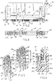
- an edge connector for use with a printed circuit board 11.
- the printed circuit board has a mating edge and a plurality of contact pads adjacent the edge.
- edge connector 10 of this invention printed circuit board 11 will have a mating edge and a plurality of contact pads 40 on both sides of the board adjacent the edge.
- This printed circuit board commonly is called the "daughter" board. In the present configuration, the contact pads on one side of the board are offset from the contact pads on the other side.
- Edge connector 10 includes an elongated dielectric housing, generally designated 12, which is fabricated of plastic material or the like.
- the housing has a plurality of depending mounting pegs 14 (Fig. 2) for insertion into appropriate mounting holes 16 in a second printed circuit board 18.
- This printed circuit board commonly is called the "mother” board, whereby edge connector 10 is effective to electrically couple circuitry of daughter board 11, through its mating edge, with circuitry of mother board 18.
- elongated housing 12 of edge connector 10 is integrally molded of the dielectric material and includes a board-receiving slot means 20 for receiving the mating edge of the daughter board.
- the slot extends, as at 20a and 20b, outwardly and upwardly into a pair of upstanding post portions 22a and 22b, respectively, of the housing.
- the connector includes an ejecting mechanism, generally designated 24, which is movable between the full-line position shown in Figure 2 to an ejecting position, shown in phantom, in order to eject the daughter board from the connector, specifically from slot 20.
- the housing has a polarizing boss 25 which is offset from a mid-point of the elongated housing for engaging in a complementary polarizing recess in the mating edge of daughter board 11 and which also is similarly offset from a mid-point of the board.
- edge connector 10 is totally omni-directional in use or application.
- a plurality of terminals are mounted on housing 12, generally within slot 20, and spaced longitudinally along the slot and housing for contacting daughter board 11 and terminating with mother board 18 in order to electrically interconnect the contact pads on the daughter board with the circuit traces on the mother board.
- each terminal 26 is edge blanked from sheet metal and includes a pair of side support portions 28a and 28b, a cross brace portion 30, a terminating portion 32 and a spring contact portion 34.
- Side support portions 28a and 28b are in the form of legs which are fixed to housing 12, within holes 36a and 36b, respectively, generally near opposite side of slot 20.
- Cross brace portion 30 extends between side support portions 28a and 28b.
- terminating portion 32 is in the form of an extension of side support portion or leg 28a to form a solder tail for insertion into an appropriate hole in mother board 18 for interconnection with a circuit trace on the mother board or in the hole thereof.
- Side support portions or legs 28a and 28b project above cross brace portion 30, as at 38a and 38b, respectively.
- leg extensions abut against side walls of housing 12 which define slot 20.
- the leg extensions are provided for facilitating top loading of the terminal into slot 20 of the housing.
- spring contact portion 34 extends from one side of the terminal (namely, from side support portion 28a), across slot 20, for engaging a contact pad 40 (Fig. 3) on an opposite side 42 of daughter board 11 adjacent mating edge 41 of the board. In the alternative, spring contact portion 34 could extend from side support portion 28b.
- housing 12 includes an area, as at 44 (Fig. 4), which supportingly engages the underside of cross brace portion 30 to resist rotational movement of the terminal as daughter board 11 biases spring contact portion 34 of the terminal transversely of slot 20. More particularly, when daughter board 11 is inserted into the connector in the direction of arrow "A" (Fig. 4), spring contact portion 34 is biased in the direction of arrow "B", resulting in an effective rotational moment of the terminal in the direction of arrow "C". Supporting area 44 of housing 12 resists this rotational moment by supportingly engaging the underside of cross brace portion 30. In addition, the interaction of the lower portion of side support 28b beneath cross brace 30 located within hole 36b further resists rotation of the terminal.
- terminals 26 be oriented along slot 20 in an alternating array along the elongated housing. Therefore, it can be seen that the contact portions of the terminals, as alternatingly arrayed in Figure 4, will be effective to alternatingly engage contact pads on opposite sides of daughter board 11. Consequently, the directions of the stresses between an individual terminal and the surrounding areas of the housing will alternate in opposite directions back-and-forth along the length of the housing, within the slot, as daughter board 11 biases the spring contact portions 34 of the terminals outwardly in alternating opposite directions.
Landscapes
- Coupling Device And Connection With Printed Circuit (AREA)
- Connector Housings Or Holding Contact Members (AREA)
Applications Claiming Priority (2)
| Application Number | Priority Date | Filing Date | Title |
|---|---|---|---|
| JP4125528A JPH05299144A (ja) | 1992-04-18 | 1992-04-18 | 電気コネクタ |
| JP125528/92 | 1992-04-18 |
Publications (2)
| Publication Number | Publication Date |
|---|---|
| EP0567006A1 true EP0567006A1 (fr) | 1993-10-27 |
| EP0567006B1 EP0567006B1 (fr) | 1997-02-26 |
Family
ID=14912413
Family Applications (1)
| Application Number | Title | Priority Date | Filing Date |
|---|---|---|---|
| EP93106204A Expired - Lifetime EP0567006B1 (fr) | 1992-04-18 | 1993-04-16 | Connecteur coopérant avec la bordure du circuit imprimé ou des dispositifs similaires |
Country Status (7)
| Country | Link |
|---|---|
| US (1) | US5259795A (fr) |
| EP (1) | EP0567006B1 (fr) |
| JP (1) | JPH05299144A (fr) |
| KR (1) | KR0122783Y1 (fr) |
| DE (1) | DE69308225T2 (fr) |
| MY (1) | MY134490A (fr) |
| SG (1) | SG44593A1 (fr) |
Cited By (4)
| Publication number | Priority date | Publication date | Assignee | Title |
|---|---|---|---|---|
| GB2270803B (en) * | 1992-09-16 | 1997-03-05 | Sumitomo Wiring Systems | Method for making a ribbon cable connector assembly |
| FR2749446A1 (fr) * | 1996-05-29 | 1997-12-05 | Cinch Connecteurs Sa | Ensemble de connexions electriques |
| CN1091309C (zh) * | 1998-03-13 | 2002-09-18 | 鸿海精密工业股份有限公司 | 电连接器组合体 |
| SG93177A1 (en) * | 1996-06-25 | 2002-12-17 | Thomas & Betts Corp | Single-sided, straddle mount printed circuit board connector (improvement) |
Families Citing this family (17)
| Publication number | Priority date | Publication date | Assignee | Title |
|---|---|---|---|---|
| US5503564A (en) * | 1992-10-30 | 1996-04-02 | The Whitaker Corporation | Assembly of an electrical connector and ejector unit for connecting IC cards to printed circuit boards |
| US5827075A (en) * | 1993-09-08 | 1998-10-27 | The Whitaker Corporation | Assembly of an electrical connector and ejector unit for connecting IC cards to printed circuit boards |
| US5514002A (en) * | 1994-04-28 | 1996-05-07 | Hon Hai Precision Ind. Co., Ltd. | Electrical connector assembly and contacts therein |
| US5713744A (en) * | 1994-09-28 | 1998-02-03 | The Whitaker Corporation | Integrated circuit socket for ball grid array and land grid array lead styles |
| US5567185A (en) * | 1994-10-19 | 1996-10-22 | Thomas & Betts Corporation | Electrical connector and method of making same |
| US5525072A (en) * | 1995-01-10 | 1996-06-11 | Molex Incorporated | Electrical connector assembly for interconnecting a flat cable to a circuit board |
| JP3362591B2 (ja) * | 1996-02-23 | 2003-01-07 | 住友電装株式会社 | フレキシブルプリント基板用コネクタ |
| JP3028199B2 (ja) * | 1996-03-14 | 2000-04-04 | モレックス インコーポレーテッド | 電気コネクタのターミナル |
| US7662093B2 (en) * | 2002-09-30 | 2010-02-16 | Given Imaging, Ltd. | Reduced size imaging device |
| US6793506B1 (en) * | 2003-08-27 | 2004-09-21 | Molex Incorporated | Board-to-board electrical connector assembly |
| JP2005129255A (ja) * | 2003-10-21 | 2005-05-19 | Three M Innovative Properties Co | コネクタ及びコネクタシステム |
| JP5694672B2 (ja) | 2010-02-25 | 2015-04-01 | スリーエム イノベイティブ プロパティズ カンパニー | 接触子および電気コネクタ |
| US8727809B2 (en) * | 2011-09-06 | 2014-05-20 | Samtec, Inc. | Center conductor with surrounding shield and edge card connector with same |
| US9077794B2 (en) | 2012-09-27 | 2015-07-07 | Tyfone, Inc. | Lightning connector accessory device |
| WO2016069570A2 (fr) | 2014-10-27 | 2016-05-06 | Fci Asia Pte. Ltd | Connecteurs d'alimentation circulaires |
| CN207338696U (zh) * | 2017-06-28 | 2018-05-08 | 安费诺商用电子产品(成都)有限公司 | 小型化高速插卡式连接器 |
| US12525755B2 (en) | 2021-07-19 | 2026-01-13 | Fci Usa Llc | Power connector for compact electronic systems |
Citations (4)
| Publication number | Priority date | Publication date | Assignee | Title |
|---|---|---|---|---|
| EP0224337A1 (fr) * | 1985-11-12 | 1987-06-03 | Amp Incorporated | Connecteur électrique pour fiche plate ou plaquette de circuit imprimé |
| US4725250A (en) * | 1987-01-27 | 1988-02-16 | Amp Incorporated | High density circuit panel socket |
| EP0356156A2 (fr) * | 1988-08-22 | 1990-02-28 | Molex Incorporated | Connecteur en bordure pour circuit imprimé et sa borne de connexion |
| EP0472203A1 (fr) * | 1990-08-23 | 1992-02-26 | The Whitaker Corporation | Socle SIMM à lecture double |
Family Cites Families (11)
| Publication number | Priority date | Publication date | Assignee | Title |
|---|---|---|---|---|
| JPS4121890Y1 (fr) * | 1964-03-23 | 1966-10-28 | ||
| US3617992A (en) * | 1968-08-26 | 1971-11-02 | Elco Corp | Swaged card-edge contact and bus strip with integral contacts |
| US3631381A (en) * | 1970-04-02 | 1971-12-28 | Ind Electronic Hardware Corp | Multiple electrical connector |
| US3732531A (en) * | 1971-06-16 | 1973-05-08 | Bunker Ramo | Electric contacts |
| US4722700A (en) * | 1987-01-23 | 1988-02-02 | Amp Incorporated | Low insertion force terminal for use with circuit panel |
| US4973270A (en) * | 1989-06-02 | 1990-11-27 | Amp Incorporated | Circuit panel socket with cloverleaf contact |
| US4960386A (en) * | 1989-10-17 | 1990-10-02 | Molex Incorporated | High deflection, high density single sided electrical connector |
| US4990107A (en) * | 1989-11-17 | 1991-02-05 | Amp Incorporated | Integrated circuit module connector assembly |
| US5104324A (en) * | 1991-06-26 | 1992-04-14 | Amp Incorporated | Multichip module connector |
| US5207598A (en) * | 1992-02-24 | 1993-05-04 | Molex Incorporated | Edge card connector |
| JP3119979B2 (ja) * | 1993-10-01 | 2000-12-25 | 株式会社奥村組 | 地下空間形成発破工法 |
-
1992
- 1992-04-18 JP JP4125528A patent/JPH05299144A/ja active Pending
- 1992-08-21 US US07/934,064 patent/US5259795A/en not_active Expired - Fee Related
- 1992-12-24 MY MYPI92002383A patent/MY134490A/en unknown
-
1993
- 1993-04-16 SG SG1996003425A patent/SG44593A1/en unknown
- 1993-04-16 DE DE69308225T patent/DE69308225T2/de not_active Expired - Fee Related
- 1993-04-16 EP EP93106204A patent/EP0567006B1/fr not_active Expired - Lifetime
- 1993-04-17 KR KR2019930006119U patent/KR0122783Y1/ko not_active Expired - Fee Related
Patent Citations (4)
| Publication number | Priority date | Publication date | Assignee | Title |
|---|---|---|---|---|
| EP0224337A1 (fr) * | 1985-11-12 | 1987-06-03 | Amp Incorporated | Connecteur électrique pour fiche plate ou plaquette de circuit imprimé |
| US4725250A (en) * | 1987-01-27 | 1988-02-16 | Amp Incorporated | High density circuit panel socket |
| EP0356156A2 (fr) * | 1988-08-22 | 1990-02-28 | Molex Incorporated | Connecteur en bordure pour circuit imprimé et sa borne de connexion |
| EP0472203A1 (fr) * | 1990-08-23 | 1992-02-26 | The Whitaker Corporation | Socle SIMM à lecture double |
Cited By (5)
| Publication number | Priority date | Publication date | Assignee | Title |
|---|---|---|---|---|
| GB2270803B (en) * | 1992-09-16 | 1997-03-05 | Sumitomo Wiring Systems | Method for making a ribbon cable connector assembly |
| FR2749446A1 (fr) * | 1996-05-29 | 1997-12-05 | Cinch Connecteurs Sa | Ensemble de connexions electriques |
| US5822197A (en) * | 1996-05-29 | 1998-10-13 | Connecteurs Cinch | Electrical connection system |
| SG93177A1 (en) * | 1996-06-25 | 2002-12-17 | Thomas & Betts Corp | Single-sided, straddle mount printed circuit board connector (improvement) |
| CN1091309C (zh) * | 1998-03-13 | 2002-09-18 | 鸿海精密工业股份有限公司 | 电连接器组合体 |
Also Published As
| Publication number | Publication date |
|---|---|
| KR930024392U (ko) | 1993-11-27 |
| MY134490A (en) | 2007-12-31 |
| SG44593A1 (en) | 1997-12-19 |
| DE69308225D1 (de) | 1997-04-03 |
| EP0567006B1 (fr) | 1997-02-26 |
| US5259795A (en) | 1993-11-09 |
| KR0122783Y1 (ko) | 1998-09-15 |
| DE69308225T2 (de) | 1997-07-31 |
| JPH05299144A (ja) | 1993-11-12 |
Similar Documents
| Publication | Publication Date | Title |
|---|---|---|
| EP0564955B1 (fr) | Connecteur de bord pour une plaquette à circuits imprimés | |
| US5259795A (en) | Edge connector for a printed circuit board or the like | |
| US4869677A (en) | Backplane connector | |
| US4655518A (en) | Backplane connector | |
| US5498167A (en) | Board to board electrical connectors | |
| US5613860A (en) | Universal grounding clip for card-receiving connector | |
| US5876222A (en) | Electrical connector for printed circuit boards | |
| US5766023A (en) | Electrical connector with high speed and high density contact strip | |
| US5259789A (en) | Retention system for circuit board mounted electrical connector | |
| US6068514A (en) | Surface mount electrical connector | |
| US5413491A (en) | Small form factor connectors with center ground plate | |
| JPH0631088U (ja) | エッジコネクタ及びそれに使用する接触子 | |
| JPH06208874A (ja) | カードリーダ用電気コネクタ | |
| MY108994A (en) | Biased edge card connector | |
| US5076804A (en) | Electrical connector assembly for mounting on a printed circuit board | |
| JPH11514131A (ja) | 応力を分離したはんだテールを有する電気コネクタ | |
| EP0122486B1 (fr) | Connecteurs électriques avec des broches quasi-terminales | |
| US5709573A (en) | Connector for high density electronic assemblies | |
| US5378175A (en) | Electrical connector for mounting on a printed circuit board | |
| US6726499B1 (en) | Electrical connector having improved terminals | |
| US6234809B1 (en) | Card connector | |
| US5236368A (en) | Printed circuit board and outrigger edge connector assembly and method of assembling the same | |
| US5601438A (en) | Independent socket for use with stacked memory card connector assembly | |
| US7014506B2 (en) | Board mounted memory card connector | |
| EP0856921A2 (fr) | Connecteur électrique pour PCB avec des éléments de retenue |
Legal Events
| Date | Code | Title | Description |
|---|---|---|---|
| PUAI | Public reference made under article 153(3) epc to a published international application that has entered the european phase |
Free format text: ORIGINAL CODE: 0009012 |
|
| AK | Designated contracting states |
Kind code of ref document: A1 Designated state(s): DE FR GB IT NL |
|
| 17P | Request for examination filed |
Effective date: 19940406 |
|
| 17Q | First examination report despatched |
Effective date: 19950814 |
|
| GRAG | Despatch of communication of intention to grant |
Free format text: ORIGINAL CODE: EPIDOS AGRA |
|
| GRAH | Despatch of communication of intention to grant a patent |
Free format text: ORIGINAL CODE: EPIDOS IGRA |
|
| ITF | It: translation for a ep patent filed | ||
| GRAH | Despatch of communication of intention to grant a patent |
Free format text: ORIGINAL CODE: EPIDOS IGRA |
|
| GRAA | (expected) grant |
Free format text: ORIGINAL CODE: 0009210 |
|
| AK | Designated contracting states |
Kind code of ref document: B1 Designated state(s): DE FR GB IT NL |
|
| REF | Corresponds to: |
Ref document number: 69308225 Country of ref document: DE Date of ref document: 19970403 |
|
| ET | Fr: translation filed | ||
| PLBE | No opposition filed within time limit |
Free format text: ORIGINAL CODE: 0009261 |
|
| 26N | No opposition filed | ||
| PGFP | Annual fee paid to national office [announced via postgrant information from national office to epo] |
Ref country code: GB Payment date: 20010313 Year of fee payment: 9 |
|
| PGFP | Annual fee paid to national office [announced via postgrant information from national office to epo] |
Ref country code: NL Payment date: 20010319 Year of fee payment: 9 |
|
| PGFP | Annual fee paid to national office [announced via postgrant information from national office to epo] |
Ref country code: FR Payment date: 20010405 Year of fee payment: 9 |
|
| PGFP | Annual fee paid to national office [announced via postgrant information from national office to epo] |
Ref country code: DE Payment date: 20010430 Year of fee payment: 9 |
|
| REG | Reference to a national code |
Ref country code: GB Ref legal event code: IF02 |
|
| PG25 | Lapsed in a contracting state [announced via postgrant information from national office to epo] |
Ref country code: GB Free format text: LAPSE BECAUSE OF NON-PAYMENT OF DUE FEES Effective date: 20020416 |
|
| PG25 | Lapsed in a contracting state [announced via postgrant information from national office to epo] |
Ref country code: NL Free format text: LAPSE BECAUSE OF NON-PAYMENT OF DUE FEES Effective date: 20021101 Ref country code: DE Free format text: LAPSE BECAUSE OF NON-PAYMENT OF DUE FEES Effective date: 20021101 |
|
| GBPC | Gb: european patent ceased through non-payment of renewal fee |
Effective date: 20020416 |
|
| PG25 | Lapsed in a contracting state [announced via postgrant information from national office to epo] |
Ref country code: FR Free format text: LAPSE BECAUSE OF NON-PAYMENT OF DUE FEES Effective date: 20021231 |
|
| NLV4 | Nl: lapsed or anulled due to non-payment of the annual fee |
Effective date: 20021101 |
|
| REG | Reference to a national code |
Ref country code: FR Ref legal event code: ST |
|
| PG25 | Lapsed in a contracting state [announced via postgrant information from national office to epo] |
Ref country code: IT Free format text: LAPSE BECAUSE OF NON-PAYMENT OF DUE FEES;WARNING: LAPSES OF ITALIAN PATENTS WITH EFFECTIVE DATE BEFORE 2007 MAY HAVE OCCURRED AT ANY TIME BEFORE 2007. THE CORRECT EFFECTIVE DATE MAY BE DIFFERENT FROM THE ONE RECORDED. Effective date: 20050416 |