EP0566258B1 - Improved slurry polisher using ultrasonic agitation - Google Patents
Improved slurry polisher using ultrasonic agitation Download PDFInfo
- Publication number
- EP0566258B1 EP0566258B1 EP93302281A EP93302281A EP0566258B1 EP 0566258 B1 EP0566258 B1 EP 0566258B1 EP 93302281 A EP93302281 A EP 93302281A EP 93302281 A EP93302281 A EP 93302281A EP 0566258 B1 EP0566258 B1 EP 0566258B1
- Authority
- EP
- European Patent Office
- Prior art keywords
- pad
- ultrasonic
- slurry
- polishing
- agitator
- Prior art date
- Legal status (The legal status is an assumption and is not a legal conclusion. Google has not performed a legal analysis and makes no representation as to the accuracy of the status listed.)
- Expired - Lifetime
Links
- 239000002002 slurry Substances 0.000 title claims description 35
- 238000013019 agitation Methods 0.000 title description 2
- 238000005498 polishing Methods 0.000 claims description 31
- 239000004065 semiconductor Substances 0.000 claims description 10
- 238000000034 method Methods 0.000 claims description 9
- 238000007517 polishing process Methods 0.000 claims 2
- 235000012431 wafers Nutrition 0.000 description 22
- 239000000463 material Substances 0.000 description 9
- VYPSYNLAJGMNEJ-UHFFFAOYSA-N Silicium dioxide Chemical compound O=[Si]=O VYPSYNLAJGMNEJ-UHFFFAOYSA-N 0.000 description 5
- 239000007788 liquid Substances 0.000 description 4
- 230000007547 defect Effects 0.000 description 3
- 230000009286 beneficial effect Effects 0.000 description 2
- 239000003989 dielectric material Substances 0.000 description 2
- 229910052451 lead zirconate titanate Inorganic materials 0.000 description 2
- 238000004519 manufacturing process Methods 0.000 description 2
- 239000000377 silicon dioxide Substances 0.000 description 2
- 235000012239 silicon dioxide Nutrition 0.000 description 2
- 241000233805 Phoenix Species 0.000 description 1
- 230000035508 accumulation Effects 0.000 description 1
- 238000009825 accumulation Methods 0.000 description 1
- 239000000853 adhesive Substances 0.000 description 1
- 229910003460 diamond Inorganic materials 0.000 description 1
- 239000010432 diamond Substances 0.000 description 1
- 238000005530 etching Methods 0.000 description 1
- 239000011810 insulating material Substances 0.000 description 1
- HFGPZNIAWCZYJU-UHFFFAOYSA-N lead zirconate titanate Chemical compound [O-2].[O-2].[O-2].[O-2].[O-2].[Ti+4].[Zr+4].[Pb+2] HFGPZNIAWCZYJU-UHFFFAOYSA-N 0.000 description 1
- 230000000873 masking effect Effects 0.000 description 1
- 239000000126 substance Substances 0.000 description 1
- 239000000725 suspension Substances 0.000 description 1
- XLYOFNOQVPJJNP-UHFFFAOYSA-N water Substances O XLYOFNOQVPJJNP-UHFFFAOYSA-N 0.000 description 1
Images
Classifications
-
- B—PERFORMING OPERATIONS; TRANSPORTING
- B24—GRINDING; POLISHING
- B24B—MACHINES, DEVICES, OR PROCESSES FOR GRINDING OR POLISHING; DRESSING OR CONDITIONING OF ABRADING SURFACES; FEEDING OF GRINDING, POLISHING, OR LAPPING AGENTS
- B24B37/00—Lapping machines or devices; Accessories
- B24B37/04—Lapping machines or devices; Accessories designed for working plane surfaces
- B24B37/07—Lapping machines or devices; Accessories designed for working plane surfaces characterised by the movement of the work or lapping tool
- B24B37/10—Lapping machines or devices; Accessories designed for working plane surfaces characterised by the movement of the work or lapping tool for single side lapping
- B24B37/105—Lapping machines or devices; Accessories designed for working plane surfaces characterised by the movement of the work or lapping tool for single side lapping the workpieces or work carriers being actively moved by a drive, e.g. in a combined rotary and translatory movement
- B24B37/107—Lapping machines or devices; Accessories designed for working plane surfaces characterised by the movement of the work or lapping tool for single side lapping the workpieces or work carriers being actively moved by a drive, e.g. in a combined rotary and translatory movement in a rotary movement only, about an axis being stationary during lapping
-
- B—PERFORMING OPERATIONS; TRANSPORTING
- B24—GRINDING; POLISHING
- B24B—MACHINES, DEVICES, OR PROCESSES FOR GRINDING OR POLISHING; DRESSING OR CONDITIONING OF ABRADING SURFACES; FEEDING OF GRINDING, POLISHING, OR LAPPING AGENTS
- B24B1/00—Processes of grinding or polishing; Use of auxiliary equipment in connection with such processes
- B24B1/04—Processes of grinding or polishing; Use of auxiliary equipment in connection with such processes subjecting the grinding or polishing tools, the abrading or polishing medium or work to vibration, e.g. grinding with ultrasonic frequency
Definitions
- This invention relates to methods of and apparatus for slurry polishing of workpieces and, more particularly, to methods of and apparatus for planarizing deposited layers on semiconductor wafers by slurry polishing.
- Slurry polishers are well known in the art and are also well known for use in planarizing deposited layers on semiconductor wafers.
- U.S. Patent No. 5,055,158 discloses a use of slurry polishing in the manufacture of Josephson integrated circuits where a deposited dielectric material is planarized so that additional layers can be deposited.
- a slurry polisher comprises a rotating horizontal pad covered by a layer of polishing slurry.
- the workpiece typically a semiconductor wafer
- the wafer itself is usually rotated at a slower rate than the pad and may also be moved radially back and forth across the rotating pad to equalize material removal from the wafer surface.
- the material of the polishing pad is chosen for its ability to act as a carrier of the slurry and to wipe away the grit and debris resulting from the polishing action.
- One particular pad material is described in U.S. Patent No. 4,927,432.
- a typical application of slurry polishing on semiconductor wafers is to planarize a deposited layer on a wafer.
- the surface of the wafer can become uneven. It may be necessary to smooth out the surface for subsequent processing steps.
- a layer of insulating or dielectric material e.g. silicon dioxide, can be deposited on the uneven surface and then polished to obtain the desired smooth surface. It is clear that such polishing operations must be carried out in such a way that scratches or other defects do not appear on the polished surface and that the material removal should preferably be extremely uniform across the surface.
- a slurry polishing pad deteriorates and must be replaced. Polishing with a deteriorated or worn pad causes more scratches and other defects as well as surface non-uniformities.
- polishing pads may have to be replaced more than once in a factory shift, which causes production bottlenecks when the polishing machine has to be taken out of use for such replacement. It is therefore desirable to find a way to prolong the life of such polishing pads to at least a full shift.
- the slurry in a slurry polisher is ultransonically agitated during polishing to dislodge embedded debris and grit from the polishing pad and thereby lengthen the life of the pad and avoid scratches, defects and non-uniform removal on the surface being polished.
- the method is particularly useful for applications in which slurry polishing is used for planarizing semiconductor wafers since surface non-uniformities can affect process yields. Apparatus is disclosed for applying ultrasonic energy to the slurry so that such energy is focussed on the pad.
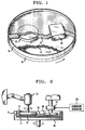
- Fig. 1 is a schematic plan view of a slurry polisher constructed in accordance with the invention.
- Fig. 2 is a partially cutaway side view of a slurry polisher showing the position of the ultrasonic apparatus used to agitate the slurry.
- Fig. 1 is a schematic plan view showing the arrangement of platen 10 of a typical commercially-available slurry polisher used for polishing semiconductor wafers and showing the position of wafer 12 being polished and ultrasonic agitator 20 positioned in accordance with the invention.
- An example of such a slurry polisher without agitator 20 is the Model 372 made by Westech Systems Inc., 3502 E. Atlanta Avenue, Phoenix, Arizona,85040.
- Fig. 2 is a partially cutaway side view of the same apparatus.
- platen 10 is mounted so that it can be rotated by a drive motor (not shown).
- Polishing pad 11 is mounted on the surface of platen 10 and rotates with it.
- These pads are typically 1.25 to 2.5mm (50 to 100 mils) thick, spongy in nature and provided with a self-adhesive backing.
- Such pads are available from Rodel Inc., 451 Belleview Road, Diamond State Industrial Park, Newark, Delaware 19713 U.S.A.
- Semiconductor wafer 12 is held from above by holder 13, which presses wafer 12 against pad 11 with a pressure typically on the order of 200 to 700 grams per cm2 (3 to 10 lbs per square inch). Holder 13 and wafer 12 are rotated by motor 14.
- motor 14 is usually mounted to apparatus that can move holder 13 to various locations to pick up wafers, clean wafers and drop off polished wafers at a point where they can proceed to the next process step.
- a layer or "lake" of polishing slurry 15 covers pad 11, typically to a depth of about 1.25 to 2.54 cms (one half to one inch).
- slurry 15 usable for polishing deposited layers on semiconductor wafers is a colloidal suspension of silica particles in a pH 8.3 to 8.7 solution of water and KOH.
- Such polishing slurries are available from Nalco Chemical Company, 6216 West 66th Place, Chicago, IL 60638 USA. Slurry 15 is kept in place by raised rim 16 on platen 10. If desired, slurry 15 can be continually replenished or recirculated from a separate reservoir (not shown).
- Ultrasonic agitator 20 has its active surface immersed in slurry 15.
- Agitator 20 is typically attached to an ultrasonic transducer 21, which is fixed to the frame of the polisher.
- Transducer 21 can be a piezoelectric material such as Lead Zirconate Titanate (PZT), and is driven by an ultrasonic generator 22, typically operating at about 40 kHz.
- PZT Lead Zirconate Titanate
- ultrasonic generator 22 typically operating at about 40 kHz.
- the pad surface improvement action can be maximized. For a 40kHz acoustic agitator this corresponds to a liquid layer that is approximately 1.25 cms (one half an inch) thick.
- planarizing In a typical application for planarizing, a layer of silicon dioxide is deposited on a semiconductor wafer, platen 10 and pad 11 are rotated at about 15 rpm and wafer 12 is rotated at about 40 rpm. Slurry 15 is typically heated to about 60 degrees C. Such planarizing operation usually takes from 5 to 8 minutes, and typically results in removal of about one ⁇ m of material from the surface of wafer 12.
- the main beneficial effect of the ultrasonic agitation of slurry 15 is to dislodge grit and debris that becomes embedded in pad 11, thereby maintaining the uniformity of the pad and the polishing operation over a longer period of time.
- An additional beneficial effect is a corresponding improvement in the effective operating lifetime of the pad.
Landscapes
- Engineering & Computer Science (AREA)
- Mechanical Engineering (AREA)
- Mechanical Treatment Of Semiconductor (AREA)
- Finish Polishing, Edge Sharpening, And Grinding By Specific Grinding Devices (AREA)
- Grinding-Machine Dressing And Accessory Apparatuses (AREA)
- Grinding And Polishing Of Tertiary Curved Surfaces And Surfaces With Complex Shapes (AREA)
Description
- This invention relates to methods of and apparatus for slurry polishing of workpieces and, more particularly, to methods of and apparatus for planarizing deposited layers on semiconductor wafers by slurry polishing.
- Slurry polishers are well known in the art and are also well known for use in planarizing deposited layers on semiconductor wafers. For example, U.S. Patent No. 5,055,158 discloses a use of slurry polishing in the manufacture of Josephson integrated circuits where a deposited dielectric material is planarized so that additional layers can be deposited.
- Typically, a slurry polisher comprises a rotating horizontal pad covered by a layer of polishing slurry. The workpiece, typically a semiconductor wafer, is pressed against the rotating pad and polishing results. The wafer itself is usually rotated at a slower rate than the pad and may also be moved radially back and forth across the rotating pad to equalize material removal from the wafer surface.
- The material of the polishing pad is chosen for its ability to act as a carrier of the slurry and to wipe away the grit and debris resulting from the polishing action. One particular pad material is described in U.S. Patent No. 4,927,432.
- A typical application of slurry polishing on semiconductor wafers is to planarize a deposited layer on a wafer. For example, after a number of processing steps, such as masking, doping, etching and the like, have been performed on the wafer, the surface of the wafer can become uneven. It may be necessary to smooth out the surface for subsequent processing steps. For this purpose, a layer of insulating or dielectric material, e.g. silicon dioxide, can be deposited on the uneven surface and then polished to obtain the desired smooth surface. It is clear that such polishing operations must be carried out in such a way that scratches or other defects do not appear on the polished surface and that the material removal should preferably be extremely uniform across the surface. Unfortunately, after a period of use, a slurry polishing pad deteriorates and must be replaced. Polishing with a deteriorated or worn pad causes more scratches and other defects as well as surface non-uniformities.
- One drawback to the use of slurry polishing is that the polishing pads may have to be replaced more than once in a factory shift, which causes production bottlenecks when the polishing machine has to be taken out of use for such replacement. It is therefore desirable to find a way to prolong the life of such polishing pads to at least a full shift.
- It is known to apply ultrasonic energy to a polishing pad to remove clogged material from the pad. For example, see Japanese Kokai Patent Application No. Sho 59[1984]-134650. In this example, a contact unit is applied to the polishing pad and ultrasonic vibrations are applied to the contact unit to break down clogged material on the pad. The contact unit is also connected to a vacuum source which removes loosened material from the pad.
- According to the present invention there is provided a method as defined in claim 1 or apparatus as defined in claim 5.
- The slurry in a slurry polisher is ultransonically agitated during polishing to dislodge embedded debris and grit from the polishing pad and thereby lengthen the life of the pad and avoid scratches, defects and non-uniform removal on the surface being polished. The method is particularly useful for applications in which slurry polishing is used for planarizing semiconductor wafers since surface non-uniformities can affect process yields. Apparatus is disclosed for applying ultrasonic energy to the slurry so that such energy is focussed on the pad.
- Fig. 1 is a schematic plan view of a slurry polisher constructed in accordance with the invention.
- Fig. 2 is a partially cutaway side view of a slurry polisher showing the position of the ultrasonic apparatus used to agitate the slurry.
- Fig. 1 is a schematic plan view showing the arrangement of
platen 10 of a typical commercially-available slurry polisher used for polishing semiconductor wafers and showing the position ofwafer 12 being polished andultrasonic agitator 20 positioned in accordance with the invention. An example of such a slurry polisher withoutagitator 20 is the Model 372 made by Westech Systems Inc., 3502 E. Atlanta Avenue, Phoenix, Arizona,85040. - Fig. 2 is a partially cutaway side view of the same apparatus.
- Referring to both Figs. 1 and 2,
platen 10 is mounted so that it can be rotated by a drive motor (not shown). Polishingpad 11 is mounted on the surface ofplaten 10 and rotates with it. These pads are typically 1.25 to 2.5mm (50 to 100 mils) thick, spongy in nature and provided with a self-adhesive backing. Such pads are available from Rodel Inc., 451 Belleview Road, Diamond State Industrial Park, Newark, Delaware 19713 U.S.A.Semiconductor wafer 12 is held from above byholder 13, which presses wafer 12 againstpad 11 with a pressure typically on the order of 200 to 700 grams per cm² (3 to 10 lbs per square inch).Holder 13 andwafer 12 are rotated bymotor 14. In practice,motor 14 is usually mounted to apparatus that can moveholder 13 to various locations to pick up wafers, clean wafers and drop off polished wafers at a point where they can proceed to the next process step. - A layer or "lake" of
polishing slurry 15 coverspad 11, typically to a depth of about 1.25 to 2.54 cms (one half to one inch). One example ofslurry 15 usable for polishing deposited layers on semiconductor wafers is a colloidal suspension of silica particles in a pH 8.3 to 8.7 solution of water and KOH. Such polishing slurries are available from Nalco Chemical Company, 6216 West 66th Place, Chicago, IL 60638 USA. Slurry 15 is kept in place by raisedrim 16 onplaten 10. If desired,slurry 15 can be continually replenished or recirculated from a separate reservoir (not shown). -
Ultrasonic agitator 20 has its active surface immersed inslurry 15.Agitator 20 is typically attached to anultrasonic transducer 21, which is fixed to the frame of the polisher.Transducer 21 can be a piezoelectric material such as Lead Zirconate Titanate (PZT), and is driven by anultrasonic generator 22, typically operating at about 40 kHz. When ultrasonic energy is applied to the transducer, acoustic power is coupled into the liquid slurry solution throughout its volume in the vicinity ofagitator 20. This energy extends, through the whole liquid layer under the agitator down to the polishing pad itself, where it tends to release accumulations of trapped grit on the pad and therefore render the pad interface more uniform. Furthermore, if the thickness of the liquid layer (between the bottom ofagitator 20 and the surface of polishing pad 11) is intentionally arranged to be an integral number of quarter wavelengths thick, then the pad surface improvement action can be maximized. For a 40kHz acoustic agitator this corresponds to a liquid layer that is approximately 1.25 cms (one half an inch) thick. - In a typical application for planarizing, a layer of silicon dioxide is deposited on a semiconductor wafer,
platen 10 andpad 11 are rotated at about 15 rpm andwafer 12 is rotated at about 40 rpm. Slurry 15 is typically heated to about 60 degrees C. Such planarizing operation usually takes from 5 to 8 minutes, and typically results in removal of about one µm of material from the surface ofwafer 12. - The main beneficial effect of the ultrasonic agitation of
slurry 15 is to dislodge grit and debris that becomes embedded inpad 11, thereby maintaining the uniformity of the pad and the polishing operation over a longer period of time. An additional beneficial effect is a corresponding improvement in the effective operating lifetime of the pad. - It is understood that other embodiments are possible that incorporate the principles of the invention as defined in the appended claims and that the above disclosure is merely illustrative of such principles.
Claims (7)
- A method of polishing a planar workpiece (12) by applying the workpiece to a rotating horizontal pad (11) at a first location whereby the motion of the pad with respect to the workpiece defines a circular path on the pad and applying ultrasonic energy to the pad at a second location on said circular path to dislodge embedded grit from said pad, said pad being covered by a layer of polishing slurry (15),
CHARACTERIZED IN THAT
said ultrasonic energy is applied to said slurry at said second location with an ultrasonic agitator (20) connected to an ultrasonic transducer (21), said ultrasonic agitator being spaced away from said pad. - The method of claim 1,
FURTHER CHARACTERIZED IN THAT
said ultrasonic agitator is positioned so that the thickness of the slurry between said ultrasonic transducer and said pad is substantially an integral number of quarter wavelengths of the frequency at which said ultrasonic transducer operates, whereby the effect of said ultrasonic energy on said pad is enhanced. - The method of claim 2,
FURTHER CHARACTERIZED IN THAT
said ultrasonic transducer operates at a frequency of about 40 kHZ and said ultrasonic agitator is spaced approximately 1.25 cm (0.5 inch) from said pad. - The method of claim 1 wherein said planar workpiece (12) is a semiconductor wafer having a deposited layer thereon,
FURTHER CHARACTERIZED IN THAT
said method of polishing is used to planarize said deposited layer. - Apparatus for polishing a planar workpiece (12) including a rotating horizontal pad (11) to which a workpiece (12) is applied at a first location whereby the motion of the pad with respect to the workpiece defines in use a circular path on said pad, means (20, 21) for applying ultrasonic energy to said pad at a second location on said path to dislodge in use embedded grit from said pad and a layer of polishing slurry (15) on said pad,
CHARACTERIZED IN THAT
said means for applying ultrasonic energy comprises an ultrasonic agitator (20) coupled to an ultrasonic transducer (21) said ultrasonic agitator being immersed in said slurry at said second location and spaced away from said pad. - The apparatus of claim 5
FURTHER CHARACTERIZED IN THAT
said ultrasonic agitator is positioned so that the thickness of the slurry between said ultrasonic transducer and said pad is substantially an integral number of quarter wavelengths of the ultrasonic frequency at which said ultrasonic transducer operates in use to thereby enhance the effect of said ultrasonic energy on said pad. - The apparatus of claim 6
FURTHER CHARACTERIZED IN THAT
said ultrasonic transducer is operated in use at a frequency of about 40 kHZ and said ultrasonic agitator is positioned approximately 1.25 cm (0.5 inch) from said pad.
Applications Claiming Priority (2)
| Application Number | Priority Date | Filing Date | Title |
|---|---|---|---|
| US07/862,044 US5245796A (en) | 1992-04-02 | 1992-04-02 | Slurry polisher using ultrasonic agitation |
| US862044 | 1992-04-02 |
Publications (2)
| Publication Number | Publication Date |
|---|---|
| EP0566258A1 EP0566258A1 (en) | 1993-10-20 |
| EP0566258B1 true EP0566258B1 (en) | 1996-06-12 |
Family
ID=25337489
Family Applications (1)
| Application Number | Title | Priority Date | Filing Date |
|---|---|---|---|
| EP93302281A Expired - Lifetime EP0566258B1 (en) | 1992-04-02 | 1993-03-25 | Improved slurry polisher using ultrasonic agitation |
Country Status (8)
| Country | Link |
|---|---|
| US (1) | US5245796A (en) |
| EP (1) | EP0566258B1 (en) |
| JP (1) | JP2981079B2 (en) |
| KR (1) | KR930022483A (en) |
| DE (1) | DE69303109T2 (en) |
| ES (1) | ES2088228T3 (en) |
| HK (1) | HK180296A (en) |
| TW (1) | TW197531B (en) |
Cited By (2)
| Publication number | Priority date | Publication date | Assignee | Title |
|---|---|---|---|---|
| US7883393B2 (en) | 2005-11-08 | 2011-02-08 | Freescale Semiconductor, Inc. | System and method for removing particles from a polishing pad |
| US8545634B2 (en) | 2005-10-19 | 2013-10-01 | Freescale Semiconductor, Inc. | System and method for cleaning a conditioning device |
Families Citing this family (95)
| Publication number | Priority date | Publication date | Assignee | Title |
|---|---|---|---|---|
| DE69317838T2 (en) * | 1992-09-24 | 1998-11-12 | Ebara Corp | Polisher |
| US5340036A (en) * | 1993-05-19 | 1994-08-23 | Emerson Electric Co. | Dry waste grinder |
| US5531861A (en) * | 1993-09-29 | 1996-07-02 | Motorola, Inc. | Chemical-mechanical-polishing pad cleaning process for use during the fabrication of semiconductor devices |
| US5456627A (en) * | 1993-12-20 | 1995-10-10 | Westech Systems, Inc. | Conditioner for a polishing pad and method therefor |
| US5551907A (en) * | 1994-03-14 | 1996-09-03 | Hughes Aircraft Company | System for ultrasonic lap grinding and polishing |
| US5783497A (en) * | 1994-08-02 | 1998-07-21 | Sematech, Inc. | Forced-flow wafer polisher |
| US5562530A (en) * | 1994-08-02 | 1996-10-08 | Sematech, Inc. | Pulsed-force chemical mechanical polishing |
| US5607341A (en) | 1994-08-08 | 1997-03-04 | Leach; Michael A. | Method and structure for polishing a wafer during manufacture of integrated circuits |
| US5522965A (en) * | 1994-12-12 | 1996-06-04 | Texas Instruments Incorporated | Compact system and method for chemical-mechanical polishing utilizing energy coupled to the polishing pad/water interface |
| US5688364A (en) * | 1994-12-22 | 1997-11-18 | Sony Corporation | Chemical-mechanical polishing method and apparatus using ultrasound applied to the carrier and platen |
| US5591068A (en) * | 1995-03-13 | 1997-01-07 | Regents Of The University Of California | Precision non-contact polishing tool |
| JP2647050B2 (en) * | 1995-03-31 | 1997-08-27 | 日本電気株式会社 | Wafer polishing equipment |
| US5672095A (en) * | 1995-09-29 | 1997-09-30 | Intel Corporation | Elimination of pad conditioning in a chemical mechanical polishing process |
| US5709593A (en) * | 1995-10-27 | 1998-01-20 | Applied Materials, Inc. | Apparatus and method for distribution of slurry in a chemical mechanical polishing system |
| KR100445139B1 (en) | 1996-01-23 | 2004-11-17 | 가부시키 가이샤 에바라 세이사꾸쇼 | Polishing apparatus |
| US5915915A (en) * | 1996-03-07 | 1999-06-29 | Komag, Incorporated | End effector and method for loading and unloading disks at a processing station |
| US5954570A (en) * | 1996-05-31 | 1999-09-21 | Kabushiki Kaisha Toshiba | Conditioner for a polishing tool |
| US5868608A (en) * | 1996-08-13 | 1999-02-09 | Lsi Logic Corporation | Subsonic to supersonic and ultrasonic conditioning of a polishing pad in a chemical mechanical polishing apparatus |
| US5932486A (en) * | 1996-08-16 | 1999-08-03 | Rodel, Inc. | Apparatus and methods for recirculating chemical-mechanical polishing of semiconductor wafers |
| US6245679B1 (en) | 1996-08-16 | 2001-06-12 | Rodel Holdings, Inc | Apparatus and methods for chemical-mechanical polishing of semiconductor wafers |
| US6210525B1 (en) | 1996-08-16 | 2001-04-03 | Rodel Holdings, Inc. | Apparatus and methods for chemical-mechanical polishing of semiconductor wafers |
| US6537137B2 (en) | 1996-08-16 | 2003-03-25 | Rodel Holdings, Inc | Methods for chemical-mechanical polishing of semiconductor wafers |
| US6769967B1 (en) | 1996-10-21 | 2004-08-03 | Micron Technology, Inc. | Apparatus and method for refurbishing polishing pads used in chemical-mechanical planarization of semiconductor wafers |
| US5782675A (en) * | 1996-10-21 | 1998-07-21 | Micron Technology, Inc. | Apparatus and method for refurbishing fixed-abrasive polishing pads used in chemical-mechanical planarization of semiconductor wafers |
| KR19980064179A (en) * | 1996-12-19 | 1998-10-07 | 윌리엄비.켐플러 | How to stabilize silicon removal rate in wafer polishing process |
| JPH10217149A (en) * | 1997-02-05 | 1998-08-18 | Ebara Corp | Cloth exfoliating jig for turntable |
| JP3130000B2 (en) | 1997-09-04 | 2001-01-31 | 松下電子工業株式会社 | Semiconductor wafer polishing apparatus and polishing method |
| US5968841A (en) * | 1997-05-06 | 1999-10-19 | International Business Machines Corporation | Device and method for preventing settlement of particles on a chemical-mechanical polishing pad |
| US5967881A (en) * | 1997-05-29 | 1999-10-19 | Tucker; Thomas N. | Chemical mechanical planarization tool having a linear polishing roller |
| US6036583A (en) * | 1997-07-11 | 2000-03-14 | Applied Materials, Inc. | Conditioner head in a substrate polisher and method |
| US5904615A (en) * | 1997-07-18 | 1999-05-18 | Hankook Machine Tools Co., Ltd. | Pad conditioner for chemical mechanical polishing apparatus |
| US5957754A (en) * | 1997-08-29 | 1999-09-28 | Applied Materials, Inc. | Cavitational polishing pad conditioner |
| DE19737849A1 (en) * | 1997-08-29 | 1999-03-11 | Siemens Ag | Device and method for heating a liquid or viscous polishing agent and device for polishing wafers |
| TW404876B (en) * | 1997-09-26 | 2000-09-11 | Siemens Ag | Process for chemical-mechanical planarization and equipment for performing said process |
| US5916010A (en) * | 1997-10-30 | 1999-06-29 | International Business Machines Corporation | CMP pad maintenance apparatus and method |
| DE69823194T2 (en) * | 1997-12-08 | 2005-04-21 | Ebara Corp | POLISHING LIQUID DISPENSER |
| US6083085A (en) | 1997-12-22 | 2000-07-04 | Micron Technology, Inc. | Method and apparatus for planarizing microelectronic substrates and conditioning planarizing media |
| JPH11277434A (en) * | 1998-03-30 | 1999-10-12 | Speedfam Co Ltd | Slurry recycle system for cmp device and method therefor |
| US6200199B1 (en) | 1998-03-31 | 2001-03-13 | Applied Materials, Inc. | Chemical mechanical polishing conditioner |
| US6024829A (en) * | 1998-05-21 | 2000-02-15 | Lucent Technologies Inc. | Method of reducing agglomerate particles in a polishing slurry |
| KR100302482B1 (en) * | 1998-06-23 | 2001-11-30 | 윤종용 | Slurry Supply System of Semiconductor CMP Process |
| US6106374A (en) * | 1998-07-16 | 2000-08-22 | International Business Machines Corporation | Acoustically agitated delivery |
| US6179693B1 (en) * | 1998-10-06 | 2001-01-30 | International Business Machines Corporation | In-situ/self-propelled polishing pad conditioner and cleaner |
| US6468139B1 (en) | 1998-12-01 | 2002-10-22 | Nutool, Inc. | Polishing apparatus and method with a refreshing polishing belt and loadable housing |
| US6589105B2 (en) | 1998-12-01 | 2003-07-08 | Nutool, Inc. | Pad tensioning method and system in a bi-directional linear polisher |
| US6103628A (en) * | 1998-12-01 | 2000-08-15 | Nutool, Inc. | Reverse linear polisher with loadable housing |
| US6464571B2 (en) | 1998-12-01 | 2002-10-15 | Nutool, Inc. | Polishing apparatus and method with belt drive system adapted to extend the lifetime of a refreshing polishing belt provided therein |
| US7425250B2 (en) * | 1998-12-01 | 2008-09-16 | Novellus Systems, Inc. | Electrochemical mechanical processing apparatus |
| JP4030247B2 (en) * | 1999-05-17 | 2008-01-09 | 株式会社荏原製作所 | Dressing device and polishing device |
| US6488569B1 (en) | 1999-07-23 | 2002-12-03 | Florida State University | Method and apparatus for detecting micro-scratches in semiconductor wafers during polishing process |
| US6306008B1 (en) | 1999-08-31 | 2001-10-23 | Micron Technology, Inc. | Apparatus and method for conditioning and monitoring media used for chemical-mechanical planarization |
| US6383934B1 (en) | 1999-09-02 | 2002-05-07 | Micron Technology, Inc. | Method and apparatus for chemical-mechanical planarization of microelectronic substrates with selected planarizing liquids |
| US6306768B1 (en) | 1999-11-17 | 2001-10-23 | Micron Technology, Inc. | Method for planarizing microelectronic substrates having apertures |
| US6313038B1 (en) | 2000-04-26 | 2001-11-06 | Micron Technology, Inc. | Method and apparatus for controlling chemical interactions during planarization of microelectronic substrates |
| US6387289B1 (en) | 2000-05-04 | 2002-05-14 | Micron Technology, Inc. | Planarizing machines and methods for mechanical and/or chemical-mechanical planarization of microelectronic-device substrate assemblies |
| US6612901B1 (en) * | 2000-06-07 | 2003-09-02 | Micron Technology, Inc. | Apparatus for in-situ optical endpointing of web-format planarizing machines in mechanical or chemical-mechanical planarization of microelectronic-device substrate assemblies |
| US6554688B2 (en) * | 2001-01-04 | 2003-04-29 | Lam Research Corporation | Method and apparatus for conditioning a polishing pad with sonic energy |
| US6875091B2 (en) * | 2001-01-04 | 2005-04-05 | Lam Research Corporation | Method and apparatus for conditioning a polishing pad with sonic energy |
| US6722943B2 (en) | 2001-08-24 | 2004-04-20 | Micron Technology, Inc. | Planarizing machines and methods for dispensing planarizing solutions in the processing of microelectronic workpieces |
| US6666749B2 (en) * | 2001-08-30 | 2003-12-23 | Micron Technology, Inc. | Apparatus and method for enhanced processing of microelectronic workpieces |
| KR20030053375A (en) * | 2001-12-22 | 2003-06-28 | 동부전자 주식회사 | Pad conditioner having a ultrasonic producing system |
| US7131889B1 (en) | 2002-03-04 | 2006-11-07 | Micron Technology, Inc. | Method for planarizing microelectronic workpieces |
| US6939203B2 (en) * | 2002-04-18 | 2005-09-06 | Asm Nutool, Inc. | Fluid bearing slide assembly for workpiece polishing |
| KR20030096766A (en) * | 2002-06-17 | 2003-12-31 | 동부전자 주식회사 | Method for stabiliting slurry by using megasonic transducer |
| US6869335B2 (en) | 2002-07-08 | 2005-03-22 | Micron Technology, Inc. | Retaining rings, planarizing apparatuses including retaining rings, and methods for planarizing micro-device workpieces |
| US7341502B2 (en) | 2002-07-18 | 2008-03-11 | Micron Technology, Inc. | Methods and systems for planarizing workpieces, e.g., microelectronic workpieces |
| US6860798B2 (en) | 2002-08-08 | 2005-03-01 | Micron Technology, Inc. | Carrier assemblies, planarizing apparatuses including carrier assemblies, and methods for planarizing micro-device workpieces |
| US7094695B2 (en) | 2002-08-21 | 2006-08-22 | Micron Technology, Inc. | Apparatus and method for conditioning a polishing pad used for mechanical and/or chemical-mechanical planarization |
| US7004817B2 (en) | 2002-08-23 | 2006-02-28 | Micron Technology, Inc. | Carrier assemblies, planarizing apparatuses including carrier assemblies, and methods for planarizing micro-device workpieces |
| US7011566B2 (en) | 2002-08-26 | 2006-03-14 | Micron Technology, Inc. | Methods and systems for conditioning planarizing pads used in planarizing substrates |
| US7008299B2 (en) | 2002-08-29 | 2006-03-07 | Micron Technology, Inc. | Apparatus and method for mechanical and/or chemical-mechanical planarization of micro-device workpieces |
| US6841991B2 (en) * | 2002-08-29 | 2005-01-11 | Micron Technology, Inc. | Planarity diagnostic system, E.G., for microelectronic component test systems |
| US7074114B2 (en) | 2003-01-16 | 2006-07-11 | Micron Technology, Inc. | Carrier assemblies, polishing machines including carrier assemblies, and methods for polishing micro-device workpieces |
| US6884152B2 (en) * | 2003-02-11 | 2005-04-26 | Micron Technology, Inc. | Apparatuses and methods for conditioning polishing pads used in polishing micro-device workpieces |
| US6872132B2 (en) | 2003-03-03 | 2005-03-29 | Micron Technology, Inc. | Systems and methods for monitoring characteristics of a polishing pad used in polishing micro-device workpieces |
| US6864181B2 (en) * | 2003-03-27 | 2005-03-08 | Lam Research Corporation | Method and apparatus to form a planarized Cu interconnect layer using electroless membrane deposition |
| US7367872B2 (en) * | 2003-04-08 | 2008-05-06 | Applied Materials, Inc. | Conditioner disk for use in chemical mechanical polishing |
| US6935929B2 (en) | 2003-04-28 | 2005-08-30 | Micron Technology, Inc. | Polishing machines including under-pads and methods for mechanical and/or chemical-mechanical polishing of microfeature workpieces |
| US7131891B2 (en) | 2003-04-28 | 2006-11-07 | Micron Technology, Inc. | Systems and methods for mechanical and/or chemical-mechanical polishing of microfeature workpieces |
| US7030603B2 (en) | 2003-08-21 | 2006-04-18 | Micron Technology, Inc. | Apparatuses and methods for monitoring rotation of a conductive microfeature workpiece |
| US7648622B2 (en) | 2004-02-27 | 2010-01-19 | Novellus Systems, Inc. | System and method for electrochemical mechanical polishing |
| US7086927B2 (en) | 2004-03-09 | 2006-08-08 | Micron Technology, Inc. | Methods and systems for planarizing workpieces, e.g., microelectronic workpieces |
| US7066792B2 (en) | 2004-08-06 | 2006-06-27 | Micron Technology, Inc. | Shaped polishing pads for beveling microfeature workpiece edges, and associate system and methods |
| US7033253B2 (en) | 2004-08-12 | 2006-04-25 | Micron Technology, Inc. | Polishing pad conditioners having abrasives and brush elements, and associated systems and methods |
| DE102004061193B3 (en) * | 2004-12-20 | 2006-07-20 | Kastriot Merlaku | Electric hand-polishing machine for polishing motor vehicles has a polishing disk, a polishing hood/gel pad and an ultrasonic drive mechanism |
| US7264539B2 (en) | 2005-07-13 | 2007-09-04 | Micron Technology, Inc. | Systems and methods for removing microfeature workpiece surface defects |
| KR100727484B1 (en) * | 2005-07-28 | 2007-06-13 | 삼성전자주식회사 | Chemical mechanical polishing apparatus and method for conditioning polishing pad |
| US7326105B2 (en) | 2005-08-31 | 2008-02-05 | Micron Technology, Inc. | Retaining rings, and associated planarizing apparatuses, and related methods for planarizing micro-device workpieces |
| US7438626B2 (en) * | 2005-08-31 | 2008-10-21 | Micron Technology, Inc. | Apparatus and method for removing material from microfeature workpieces |
| US7294049B2 (en) | 2005-09-01 | 2007-11-13 | Micron Technology, Inc. | Method and apparatus for removing material from microfeature workpieces |
| US7754612B2 (en) | 2007-03-14 | 2010-07-13 | Micron Technology, Inc. | Methods and apparatuses for removing polysilicon from semiconductor workpieces |
| JP2010179407A (en) * | 2009-02-05 | 2010-08-19 | Elpida Memory Inc | Cmp device |
| US20110169520A1 (en) * | 2010-01-14 | 2011-07-14 | Mks Instruments, Inc. | Apparatus for measuring minority carrier lifetime and method for using the same |
| JP7134101B2 (en) | 2016-06-24 | 2022-09-09 | アプライド マテリアルズ インコーポレイテッド | Slurry distributor for chemical mechanical polishing |
| US10391609B1 (en) * | 2017-09-05 | 2019-08-27 | Optipro Systems, LLC | Modular contact assembly for rotating machine tool |
Family Cites Families (14)
| Publication number | Priority date | Publication date | Assignee | Title |
|---|---|---|---|---|
| US3123951A (en) * | 1964-03-10 | Ultrasonic cleaning of grinding wheels | ||
| US3093937A (en) * | 1962-11-30 | 1963-06-18 | Cavitron Ultrasonics Inc | Ultrasonic lapping machines |
| US3855441A (en) * | 1974-04-08 | 1974-12-17 | Braelow D | Method and apparatus for activation of an abrasive slurry by an electric arc |
| DE2435848C3 (en) * | 1974-07-25 | 1979-07-26 | Supfina Maschinenfabrik Hentzen Kg, 5630 Remscheid | Device for keeping the contact surface of a honing stone clean |
| US4069805A (en) * | 1977-01-25 | 1978-01-24 | Philip Sherman | Wire apparatus for abrasive powder machining |
| US4927432A (en) * | 1986-03-25 | 1990-05-22 | Rodel, Inc. | Pad material for grinding, lapping and polishing |
| DE3625286A1 (en) * | 1986-07-25 | 1988-02-04 | Flier Gustav | Cleaning of grinding wheels by subjecting the cooling water to ultrasound, in particular for grinding machines |
| JPS6362673A (en) * | 1986-09-01 | 1988-03-18 | Speedfam Co Ltd | Surface polishing machine associated with fixed dimension mechanism |
| JPS63185556A (en) * | 1987-01-28 | 1988-08-01 | Toshiba Corp | Polishing device |
| AU619263B2 (en) * | 1988-03-10 | 1992-01-23 | Extrude Hone Corporation | Ultrasonic polishing |
| US5104828A (en) * | 1990-03-01 | 1992-04-14 | Intel Corporation | Method of planarizing a dielectric formed over a semiconductor substrate |
| US5055158A (en) * | 1990-09-25 | 1991-10-08 | International Business Machines Corporation | Planarization of Josephson integrated circuit |
| US5154021A (en) * | 1991-06-26 | 1992-10-13 | International Business Machines Corporation | Pneumatic pad conditioner |
| US5245790A (en) * | 1992-02-14 | 1993-09-21 | Lsi Logic Corporation | Ultrasonic energy enhanced chemi-mechanical polishing of silicon wafers |
-
1992
- 1992-04-02 US US07/862,044 patent/US5245796A/en not_active Expired - Lifetime
- 1992-05-13 TW TW081103708A patent/TW197531B/zh not_active IP Right Cessation
-
1993
- 1993-03-25 DE DE69303109T patent/DE69303109T2/en not_active Expired - Fee Related
- 1993-03-25 EP EP93302281A patent/EP0566258B1/en not_active Expired - Lifetime
- 1993-03-25 ES ES93302281T patent/ES2088228T3/en not_active Expired - Lifetime
- 1993-03-30 KR KR1019930005069A patent/KR930022483A/en not_active Application Discontinuation
- 1993-04-02 JP JP9844393A patent/JP2981079B2/en not_active Expired - Lifetime
-
1996
- 1996-09-26 HK HK180296A patent/HK180296A/en not_active IP Right Cessation
Cited By (2)
| Publication number | Priority date | Publication date | Assignee | Title |
|---|---|---|---|---|
| US8545634B2 (en) | 2005-10-19 | 2013-10-01 | Freescale Semiconductor, Inc. | System and method for cleaning a conditioning device |
| US7883393B2 (en) | 2005-11-08 | 2011-02-08 | Freescale Semiconductor, Inc. | System and method for removing particles from a polishing pad |
Also Published As
| Publication number | Publication date |
|---|---|
| HK180296A (en) | 1996-10-04 |
| KR930022483A (en) | 1993-11-24 |
| EP0566258A1 (en) | 1993-10-20 |
| DE69303109T2 (en) | 1996-10-10 |
| ES2088228T3 (en) | 1996-08-01 |
| TW197531B (en) | 1993-01-01 |
| JP2981079B2 (en) | 1999-11-22 |
| US5245796A (en) | 1993-09-21 |
| DE69303109D1 (en) | 1996-07-18 |
| JPH068134A (en) | 1994-01-18 |
Similar Documents
| Publication | Publication Date | Title |
|---|---|---|
| EP0566258B1 (en) | Improved slurry polisher using ultrasonic agitation | |
| US5531861A (en) | Chemical-mechanical-polishing pad cleaning process for use during the fabrication of semiconductor devices | |
| US7951718B2 (en) | Edge removal of silicon-on-insulator transfer wafer | |
| US5860181A (en) | Method of and apparatus for cleaning workpiece | |
| US6361413B1 (en) | Apparatus and methods for conditioning polishing pads in mechanical and/or chemical-mechanical planarization of microelectronic device substrate assemblies | |
| KR100750771B1 (en) | Vacuum-assisted pad conditioning method utilizing an apertured conditioning disk | |
| US8485863B2 (en) | Polishing liquids for activating and/or conditioning fixed abrasive polishing pads, and associated systems and methods | |
| KR100574323B1 (en) | Semiconductor equipment fabrication method and working apparatus | |
| US6022266A (en) | In-situ pad conditioning process for CMP | |
| EP1052062A1 (en) | Pré-conditioning fixed abrasive articles | |
| KR20060050007A (en) | Polishing pad conditioner and methods of manufacture and recycling | |
| KR19980087365A (en) | Semiconductor polishing method and apparatus | |
| US6149505A (en) | Cavitational polishing pad conditioner | |
| US6855043B1 (en) | Carrier head with a modified flexible membrane | |
| JP4104950B2 (en) | Substrate polishing method | |
| JPH10256201A (en) | Manufacturing method of semiconductor | |
| JPH1110526A (en) | Substrate polishing device and substrate polishing method | |
| EP0750968B1 (en) | Apparatus for conditioning a polishing pad | |
| JP2001274123A (en) | Substrate polishing apparatus and substrate-polishing method | |
| KR20070024145A (en) | Cmp apparatus for semiconductor device manufacturing | |
| KR20050068759A (en) | Slurry exclusion device and method of carrier film at cmp process |
Legal Events
| Date | Code | Title | Description |
|---|---|---|---|
| PUAI | Public reference made under article 153(3) epc to a published international application that has entered the european phase |
Free format text: ORIGINAL CODE: 0009012 |
|
| AK | Designated contracting states |
Kind code of ref document: A1 Designated state(s): DE ES FR GB IT NL |
|
| 17P | Request for examination filed |
Effective date: 19940331 |
|
| RAP3 | Party data changed (applicant data changed or rights of an application transferred) |
Owner name: AT&T CORP. |
|
| 17Q | First examination report despatched |
Effective date: 19950117 |
|
| GRAH | Despatch of communication of intention to grant a patent |
Free format text: ORIGINAL CODE: EPIDOS IGRA |
|
| GRAH | Despatch of communication of intention to grant a patent |
Free format text: ORIGINAL CODE: EPIDOS IGRA |
|
| GRAA | (expected) grant |
Free format text: ORIGINAL CODE: 0009210 |
|
| AK | Designated contracting states |
Kind code of ref document: B1 Designated state(s): DE ES FR GB IT NL |
|
| ITF | It: translation for a ep patent filed | ||
| ET | Fr: translation filed | ||
| REG | Reference to a national code |
Ref country code: ES Ref legal event code: BA2A Ref document number: 2088228 Country of ref document: ES Kind code of ref document: T3 |
|
| REF | Corresponds to: |
Ref document number: 69303109 Country of ref document: DE Date of ref document: 19960718 |
|
| REG | Reference to a national code |
Ref country code: ES Ref legal event code: FG2A Ref document number: 2088228 Country of ref document: ES Kind code of ref document: T3 |
|
| PLBE | No opposition filed within time limit |
Free format text: ORIGINAL CODE: 0009261 |
|
| STAA | Information on the status of an ep patent application or granted ep patent |
Free format text: STATUS: NO OPPOSITION FILED WITHIN TIME LIMIT |
|
| 26N | No opposition filed | ||
| PGFP | Annual fee paid to national office [announced via postgrant information from national office to epo] |
Ref country code: GB Payment date: 20010226 Year of fee payment: 9 |
|
| PGFP | Annual fee paid to national office [announced via postgrant information from national office to epo] |
Ref country code: ES Payment date: 20010302 Year of fee payment: 9 |
|
| PGFP | Annual fee paid to national office [announced via postgrant information from national office to epo] |
Ref country code: NL Payment date: 20010312 Year of fee payment: 9 |
|
| PGFP | Annual fee paid to national office [announced via postgrant information from national office to epo] |
Ref country code: DE Payment date: 20010330 Year of fee payment: 9 |
|
| REG | Reference to a national code |
Ref country code: GB Ref legal event code: IF02 |
|
| PG25 | Lapsed in a contracting state [announced via postgrant information from national office to epo] |
Ref country code: GB Free format text: LAPSE BECAUSE OF NON-PAYMENT OF DUE FEES Effective date: 20020325 |
|
| PG25 | Lapsed in a contracting state [announced via postgrant information from national office to epo] |
Ref country code: ES Free format text: LAPSE BECAUSE OF NON-PAYMENT OF DUE FEES Effective date: 20020326 |
|
| PG25 | Lapsed in a contracting state [announced via postgrant information from national office to epo] |
Ref country code: NL Free format text: LAPSE BECAUSE OF NON-PAYMENT OF DUE FEES Effective date: 20021001 Ref country code: DE Free format text: LAPSE BECAUSE OF NON-PAYMENT OF DUE FEES Effective date: 20021001 |
|
| GBPC | Gb: european patent ceased through non-payment of renewal fee |
Effective date: 20020325 |
|
| NLV4 | Nl: lapsed or anulled due to non-payment of the annual fee |
Effective date: 20021001 |
|
| REG | Reference to a national code |
Ref country code: ES Ref legal event code: FD2A Effective date: 20030410 |
|
| PG25 | Lapsed in a contracting state [announced via postgrant information from national office to epo] |
Ref country code: IT Free format text: LAPSE BECAUSE OF NON-PAYMENT OF DUE FEES;WARNING: LAPSES OF ITALIAN PATENTS WITH EFFECTIVE DATE BEFORE 2007 MAY HAVE OCCURRED AT ANY TIME BEFORE 2007. THE CORRECT EFFECTIVE DATE MAY BE DIFFERENT FROM THE ONE RECORDED. Effective date: 20050325 |
|
| PGFP | Annual fee paid to national office [announced via postgrant information from national office to epo] |
Ref country code: FR Payment date: 20120403 Year of fee payment: 20 |