EP0565276A2 - Free-space optical switching apparatus - Google Patents
Free-space optical switching apparatus Download PDFInfo
- Publication number
- EP0565276A2 EP0565276A2 EP93302282A EP93302282A EP0565276A2 EP 0565276 A2 EP0565276 A2 EP 0565276A2 EP 93302282 A EP93302282 A EP 93302282A EP 93302282 A EP93302282 A EP 93302282A EP 0565276 A2 EP0565276 A2 EP 0565276A2
- Authority
- EP
- European Patent Office
- Prior art keywords
- component
- switching apparatus
- optical
- photo
- optical switching
- Prior art date
- Legal status (The legal status is an assumption and is not a legal conclusion. Google has not performed a legal analysis and makes no representation as to the accuracy of the status listed.)
- Granted
Links
Images


Classifications
-
- G—PHYSICS
- G02—OPTICS
- G02B—OPTICAL ELEMENTS, SYSTEMS OR APPARATUS
- G02B6/00—Light guides; Structural details of arrangements comprising light guides and other optical elements, e.g. couplings
- G02B6/24—Coupling light guides
- G02B6/26—Optical coupling means
- G02B6/35—Optical coupling means having switching means
- G02B6/3586—Control or adjustment details, e.g. calibrating
- G02B6/3588—Control or adjustment details, e.g. calibrating of the processed beams, i.e. controlling during switching of orientation, alignment, or beam propagation properties such as intensity, size or shape
-
- G—PHYSICS
- G02—OPTICS
- G02B—OPTICAL ELEMENTS, SYSTEMS OR APPARATUS
- G02B6/00—Light guides; Structural details of arrangements comprising light guides and other optical elements, e.g. couplings
- G02B6/24—Coupling light guides
- G02B6/26—Optical coupling means
- G02B6/35—Optical coupling means having switching means
- G02B6/3502—Optical coupling means having switching means involving direct waveguide displacement, e.g. cantilever type waveguide displacement involving waveguide bending, or displacing an interposed waveguide between stationary waveguides
-
- G—PHYSICS
- G02—OPTICS
- G02B—OPTICAL ELEMENTS, SYSTEMS OR APPARATUS
- G02B6/00—Light guides; Structural details of arrangements comprising light guides and other optical elements, e.g. couplings
- G02B6/24—Coupling light guides
- G02B6/26—Optical coupling means
- G02B6/35—Optical coupling means having switching means
- G02B6/354—Switching arrangements, i.e. number of input/output ports and interconnection types
- G02B6/3544—2D constellations, i.e. with switching elements and switched beams located in a plane
- G02B6/3548—1xN switch, i.e. one input and a selectable single output of N possible outputs
Definitions
- the invention relates to optical switching apparatus and, more particularly, to a free-space optical cross-connect switching apparatus.
- One method of switching an optical signal from one path to another is by means of an optical cross-connect switch.
- free-space optical cross-connect switches perform this switching by redirecting an information-bearing collimated laser beams from one route to another as the light traverses a free-space path. This re-direction is accomplished by varying the trajectory on which the collimated laser beams is launched into the free-space path, so that it exits on a different route from the opposite end of the free-space path.
- Prior free-space optical cross-connect switches employ schemes for varying the launch trajectory of a collimated laser beam that require the use of a companion pilot beam for each information- bearing beam being launched.
- Each of these pilot beams is aligned with a specific information-bearing beam and employed to guide that beam onto a photo-receptor which serves as a gateway to the desired exit route.
- each photo-receptor is situated at the center of an array of photo-detectors.
- a particular information-bearing beam, along with its companion pilot beam is launched toward a particular photo- receptor.
- the surrounding photo-detectors sense the pilot beam, and provide feedback to a controller which directs the information-bearing beam directly onto the proper photo-receptor.
- the present invention overcomes the deficiencies of prior free- space optical cross-connect switches by adjusting the launch trajectory of an information-bearing collimated laser beam in response to the position of a monitor component beam derived from a launched information bearing beam.
- Two component beams are obtained from the information-bearing beam: a payload component beam and a monitor component beam.
- Each component beam is derived in a manner which insures that its trajectory is directly related to the trajectory of the launched information-bearing beam.
- the payload component of the beam is directed onto a photo-receptor, and the monitor component is directed toward a photo-sensor.
- the launch trajectory of the information-bearing beam is adjusted in response to feedback received from the photo- sensor, this feedback being indicative of the monitor component beam position.
- the position of the monitor component beam is directly related to that of the payload component beam . More specifically, target regions are designated upon the photo-sensor so thatwhen the mon- itorcomponent beam is positioned upon a given target region, the associated payload component beam is positioned upon a corresponding photo-receptor.
- a controller receives positional information from the photo-sensor and, responsively, adjusts the launch trajectory of the information-bearing beam so as to cause the monitorcom- ponent beam derived from the launched beam to be incident upon a specific target region. Thus the associated payload component is made incident upon a corresponding photo-receptor.
- the monitor component beam is proportional to the payload component beam in both intensity and cross-sectional profile. This allows the photo-sensor to collect information indicative of payload component beam quality, thus providing a continuous and operationally transparent method of monitoring critical payload component beam characteristics.
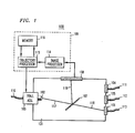
- FIG. 1 shows, in simplified form, a preferred embodiment of the invention. Specifically, shown is optical switching apparatus 100, having free-space optical path 101. Collimated beam launcher 102 and beam trajectory adjusting means 103 are located at one end of free-space optical path 101. Photo-receptors 104, 105 and 106 are located at the opposite end of free-space optical path 101. Also shown, are partially-silvered mirror 107, CCD area sensor 108, processor/controller 109, and optical fibers 110, 111, 112, and 113. As illustrated in FIG. 1, processor/controller 109 is comprised of image processor 114, trajectory processor 115, and memory 116.
- optical fiber 110 delivers collimated laser beam 117 to beam launcher 102, which launches the beam into free-space optical path 101 toward photo-receptors 104, 105 and 106.
- the position of beam trajectory adjusting means 103 determines the particular trajectory the beam will have as it enters free-space optical path 101.
- Methods of adjusting the trajectory of a laser beam as it exits an optical fiber are well known in the art; they include servo-controlled motor and piezo-electric driven positioning means.
- the particular trajectory adjusting method employed is not critical, so long as rapid and accurate adjustments may be made in response to a control signal received from processor/controller 109.
- Partially-silvered mirror 107 is positioned within free-space optical path 101 so that it lies in the path of collimated laser beam 117. A portion of laser beam 117 passes unobstructed through mirror 107, exiting as payload beam component 118. Another portion of beam 117 is reflected off of mirror 107 as monitor beam component 119. CCD area sensor 108 is positioned so that monitor beam component 119 will be incident upon its surface. The trajectory of payload beam component 118 and monitor beam component 119 are both functions of the trajectory of collimated laser beam 117.
- CCD area sensor 108 the location at which monitor beam component 119 strikes the surface of CCD area sensor 108 is directly related to the location at which payload beam component 118 is incident upon the end of free-space optical path 101 housing photo-receptors 104, 105 and 106.
- the sensitivity of CCD sensor 108 facilitates the accurate detection of monitor beams having relatively low intensities. This allows partially silvered mirror 107 to be configured so that close to 100% of collimated laser beam 117 exits unobstructed as payload beam 118, thereby minimizing optical losses within switching apparatus 100.
- CCD area sensor 108 Specific sections of CCD area sensor 108 are designated as target regions. These target regions are chosen so that when payload beam component 118 is incident upon a particular photo-receptor, monitor beam component 119 will be incident upon an corresponding target region.
- FIG. 2 provides a detailed illustration of the surface of CCD area sensor 108.
- CCD area sensors are comprised of a matrix of discrete photo-sensitive elements 201.
- Area sensor 108 is shown to be a 256 x 256 matrix of elements; each element being represented as a rectangular region upon the surface of the sensor.
- Individual photo-sensitive elements are identified by an address consisting of a column and row number (for purposes of illustration, the column and row numbers are shown in FIG. 2).
- the target regions associated with photo-receptors 104,105 and 106 are indicated by the dotted-line circles 204, 205 and 206, respectively. These target regions are configured so they are slightly larger than the area upon CCD sensor 108 illuminated by a given monitor beam component (the profile of incident monitor beam component 119 is shown a shaded circular area in FIG. 2).
- the addresses of the elements within each of these target regions are stored in memory 116.
- processor/controller 109 adjusts the trajectory of beam 117 so that payload beam component 118 is directed onto a particular photo-receptor, thereby channeling the beam into an optical fiber and effecting an optical cross-connect.
- processor/controller 109 would receive the request to execute a particular cross-connect from a network manager or other processor which controls signal routing.
- image processor 114 scans CCD area sensor 108 and determines addresses of the elements which monitor beam component 119 (represented by the shaded circular area within target region 206) is incident upon. These addresses are passed to trajectory processor 115, which compares them to the element addresses for the target region corresponding to the particular photo-receptor to which payload beam component 118 is to be directed.
- Trajectory processor 115 then transmits a control signal to beam trajectory adjusting means 103 so as to alter the launch trajectory of collimated laser beam 117 and, thereby cause monitor beam component 119 to be incident upon the elements associated with the desired target location. Feedback on the position of monitor beam component 119 is received by trajectory processor 115 in the form of the addresses of the elements upon which monitor beam component 119 is incident. This feedback enables trajectory processor 115 to monitor and correct any errors in the positioning of beam 117 and, hence, payload beam component 118.
- an unintentional optical connection may result.
- Translating monitor beams component 119 from target region 206 to target region 204, via the shortest path (shown as shaded arrow 301), would result in the monitor beam component passing directly across target region 205.
- trajectory processor 115 is programmed to direct the monitor beam component around elements associated with non-destination target regions (see shaded arrow 302).
- CCD area sensor in this particular embodiment of the invention, one of which is the elimination of "blind spots".
- image processor 114 is provided with information as to the position of the monitor beam component 119 anywhere on the CCD's surface - not just over or near specific target regions. This reduces the likehood of the processor/controller 109 being left “blind” as to the location of the monitor beam component.
- CCD area sensor 108 enables processor/controller 109 to monitor payload beam component quality as a function of monitor beam component quality.
- CCD sensor 108 is configured so that the cross- sectional profile of monitor beam component 119 traverses a plurality of individual elements.
- Image processor 114 collects information indicative of the average intensity of monitor beam component 119 incident upon the elements of CCD area sensor 108. This intensity information, which provides an accurate indication of the effective power and cross-sectional profile of monitor beam component 119, is passed from image processor 114 to trajectory processor 115.
- Trajectory processor 115 compares the received information with profile and intensity standards stored in memory 116, thus allowing the detection of undesirable fluctuations in beam quality.
- the quality of the monitor beam component provides an accurate measure of payload beam component quality.
- FIG. 4 Another embodiment of the invention is shown in FIG. 4. Specifically, shown is optical switching apparatus 400, having free-space optical path 101. Collimated beam launcher 102 and beam trajectory adjusting means 103 are located at one end of free-space optical path 101; photo-receptors 404,405 and 406 located at an opposite end. Also shown are partially-silvered mirror 107, CCD area sensor 108, processor/controller 109, and transmission means 410, 411, 412, and 413. As illustrated in FIG. 4, processor/controller 109 is comprised of image processor 114, trajectory processor 115, and memory 116.
- an electrical signal as opposed to an optical signal, is delivered to optical switching apparatus 400.
- This electrical signal is delivered via transmission means 410, to laser402.
- Laser 402 produces a collimated beam 117 in response to the delivered electrical signal, and launches that beam into free- space optical path 101 toward photo-receptors 404, 405 and 406.
- photo-receptors 404, 405, and 406 do not channel incident payload component beams into optical fibers. Rather, each of the photo-receptors 404,405 and 406 generates an electrical signal in response to incident laser beams .
- These electrical signals are carried out of the optical switching apparatus 400 via electrical transmission means 411, 412, and 413.
- On such modification might include an optical switching apparatus having a plurality of independently controllable collimated laser beam launchers, each being responsive to a control signal from a processor/controller.
Abstract
Description
- The invention relates to optical switching apparatus and, more particularly, to a free-space optical cross-connect switching apparatus.
- One method of switching an optical signal from one path to another is by means of an optical cross-connect switch. In particular, free-space optical cross-connect switches perform this switching by redirecting an information-bearing collimated laser beams from one route to another as the light traverses a free-space path. This re-direction is accomplished by varying the trajectory on which the collimated laser beams is launched into the free-space path, so that it exits on a different route from the opposite end of the free-space path.
- Prior free-space optical cross-connect switches employ schemes for varying the launch trajectory of a collimated laser beam that require the use of a companion pilot beam for each information- bearing beam being launched. Each of these pilot beams is aligned with a specific information-bearing beam and employed to guide that beam onto a photo-receptor which serves as a gateway to the desired exit route. Typically, each photo-receptor is situated at the center of an array of photo-detectors. In operation, a particular information-bearing beam, along with its companion pilot beam , is launched toward a particular photo- receptor. The surrounding photo-detectors sense the pilot beam, and provide feedback to a controller which directs the information-bearing beam directly onto the proper photo-receptor.
- While this type of free-space optical cross-connect switch has proved effective, it requires a significant amount of hardware to implement the pilot beam system. In addition, as the pilot beam provides the sole means for insuring proper targeting of the information-bearing beam, misalignment between the pilot and information-bearing beams could result in a failed cross- connection. Another drawback of this type of optical cross- connect switch is the limited ability of the photo-detectors to locate the pilot beam . If a pilot beam is not incident upon one of the photo-detectors, the cross-connect switch is left "blind" as to the location of the pilot beam. This deprives the controller of any feedback to aid in properly targeting the information-bearing beam associated with the pilot beam.
- The present invention overcomes the deficiencies of prior free- space optical cross-connect switches by adjusting the launch trajectory of an information-bearing collimated laser beam in response to the position of a monitor component beam derived from a launched information bearing beam. Two component beams are obtained from the information-bearing beam: a payload component beam and a monitor component beam. Each component beam is derived in a manner which insures that its trajectory is directly related to the trajectory of the launched information-bearing beam. The payload component of the beam is directed onto a photo-receptor, and the monitor component is directed toward a photo-sensor. The launch trajectory of the information-bearing beam is adjusted in response to feedback received from the photo- sensor, this feedback being indicative of the monitor component beam position.
- As the trajectories of both component beams are directly related to that of the launched information-bearing beam, the position of the monitor component beam is directly related to that of the payload component beam . More specifically, target regions are designated upon the photo-sensor so thatwhen the mon- itorcomponent beam is positioned upon a given target region, the associated payload component beam is positioned upon a corresponding photo-receptor. In accordance with the invention, a controller receives positional information from the photo-sensor and, responsively, adjusts the launch trajectory of the information-bearing beam so as to cause the monitorcom- ponent beam derived from the launched beam to be incident upon a specific target region. Thus the associated payload component is made incident upon a corresponding photo-receptor.
- In a particular embodiment of the invention, the monitor component beam is proportional to the payload component beam in both intensity and cross-sectional profile. This allows the photo-sensor to collect information indicative of payload component beam quality, thus providing a continuous and operationally transparent method of monitoring critical payload component beam characteristics.
- In the drawing:
- FIG. 1 shows, in simplified form, a free-space optical switching apparatus including an embodiment of the invention;
- FIG. 2 shows a frontal view of the charge-coupled device ("CCD") area sensor of FIG. 1;
- FIG. 3 shows the path of a collimated beam across the surface of the CCD area sensor of FIG. 1; and
- FIG. 4 shows, in simplified form, a free-space optical switching apparatus including a second embodiment of the invention.
- FIG. 1 shows, in simplified form, a preferred embodiment of the invention. Specifically, shown is
optical switching apparatus 100, having free-spaceoptical path 101. Collimatedbeam launcher 102 and beam trajectory adjusting means 103 are located at one end of free-spaceoptical path 101. Photo-receptors optical path 101. Also shown, are partially-silvered mirror 107,CCD area sensor 108, processor/controller 109, andoptical fibers controller 109 is comprised ofimage processor 114,trajectory processor 115, andmemory 116. - In this particular embodiment,
optical fiber 110 delivers collimatedlaser beam 117 tobeam launcher 102, which launches the beam into free-spaceoptical path 101 toward photo-receptors optical path 101. Methods of adjusting the trajectory of a laser beam as it exits an optical fiber are well known in the art; they include servo-controlled motor and piezo-electric driven positioning means. The particular trajectory adjusting method employed is not critical, so long as rapid and accurate adjustments may be made in response to a control signal received from processor/controller 109. - Partially-
silvered mirror 107 is positioned within free-spaceoptical path 101 so that it lies in the path of collimatedlaser beam 117. A portion oflaser beam 117 passes unobstructed throughmirror 107, exiting aspayload beam component 118. Another portion ofbeam 117 is reflected off ofmirror 107 asmonitor beam component 119.CCD area sensor 108 is positioned so thatmonitor beam component 119 will be incident upon its surface. The trajectory ofpayload beam component 118 andmonitor beam component 119 are both functions of the trajectory of collimatedlaser beam 117. As a result, the location at whichmonitor beam component 119 strikes the surface ofCCD area sensor 108 is directly related to the location at whichpayload beam component 118 is incident upon the end of free-spaceoptical path 101 housing photo-receptors CCD sensor 108 facilitates the accurate detection of monitor beams having relatively low intensities. This allows partiallysilvered mirror 107 to be configured so that close to 100% of collimatedlaser beam 117 exits unobstructed aspayload beam 118, thereby minimizing optical losses within switchingapparatus 100. - Specific sections of
CCD area sensor 108 are designated as target regions. These target regions are chosen so that whenpayload beam component 118 is incident upon a particular photo-receptor,monitor beam component 119 will be incident upon an corresponding target region. FIG. 2 provides a detailed illustration of the surface ofCCD area sensor 108. Typically, such CCD area sensors are comprised of a matrix of discrete photo-sensitive elements 201.Area sensor 108 is shown to be a 256 x 256 matrix of elements; each element being represented as a rectangular region upon the surface of the sensor. Individual photo-sensitive elements are identified by an address consisting of a column and row number (for purposes of illustration, the column and row numbers are shown in FIG. 2). The target regions associated with photo-receptors 104,105 and 106 (FIG. 1) are indicated by the dotted-line circles CCD sensor 108 illuminated by a given monitor beam component (the profile of incidentmonitor beam component 119 is shown a shaded circular area in FIG. 2). The addresses of the elements within each of these target regions are stored inmemory 116. - In operation, processor/
controller 109 adjusts the trajectory ofbeam 117 so thatpayload beam component 118 is directed onto a particular photo-receptor, thereby channeling the beam into an optical fiber and effecting an optical cross-connect. Typically, processor/controller 109 would receive the request to execute a particular cross-connect from a network manager or other processor which controls signal routing. To effect the cross- connect,image processor 114 scansCCD area sensor 108 and determines addresses of the elements which monitor beam component 119 (represented by the shaded circular area within target region 206) is incident upon. These addresses are passed totrajectory processor 115, which compares them to the element addresses for the target region corresponding to the particular photo-receptor to whichpayload beam component 118 is to be directed.Trajectory processor 115 then transmits a control signal to beam trajectory adjusting means 103 so as to alter the launch trajectory of collimatedlaser beam 117 and, thereby causemonitor beam component 119 to be incident upon the elements associated with the desired target location. Feedback on the position ofmonitor beam component 119 is received bytrajectory processor 115 in the form of the addresses of the elements upon which monitorbeam component 119 is incident. This feedback enablestrajectory processor 115 to monitor and correct any errors in the positioning ofbeam 117 and, hence,payload beam component 118. - In the process of causing
monitor beam component 119 to coincide with a desired target region, an unintentional optical connection may result. For example, as shown in FIG. 3, translatingmonitor beams component 119 fromtarget region 206 to targetregion 204, via the shortest path (shown as shaded arrow 301), would result in the monitor beam component passing directly acrosstarget region 205. This would causepayload beam component 118 to pass over photo-receptor 105, and an unintentional cross-connect to be temporarily established as the beam was channeled intooptical fiber 112. To insure that such unitentional channeling does not take place,trajectory processor 115 is programmed to direct the monitor beam component around elements associated with non-destination target regions (see shaded arrow 302). - Several advantages are offered by the use of a CCD area sensor in this particular embodiment of the invention; one of which is the elimination of "blind spots". As Almost the entire surface of
CCD 108 is photo-sensitive,image processor 114 is provided with information as to the position of themonitor beam component 119 anywhere on the CCD's surface - not just over or near specific target regions. This reduces the likehood of the processor/controller 109 being left "blind" as to the location of the monitor beam component. - In addition, the resolution and light sensitivity of
CCD area sensor 108 enables processor/controller 109 to monitor payload beam component quality as a function of monitor beam component quality.CCD sensor 108 is configured so that the cross- sectional profile ofmonitor beam component 119 traverses a plurality of individual elements.Image processor 114 collects information indicative of the average intensity ofmonitor beam component 119 incident upon the elements ofCCD area sensor 108. This intensity information, which provides an accurate indication of the effective power and cross-sectional profile ofmonitor beam component 119, is passed fromimage processor 114 totrajectory processor 115.Trajectory processor 115 compares the received information with profile and intensity standards stored inmemory 116, thus allowing the detection of undesirable fluctuations in beam quality. As both monitorbeam component 119 andpayload beam component 118 originate from the same collimatedlaser beam 117, the quality of the monitor beam component provides an accurate measure of payload beam component quality. - Another embodiment of the invention is shown in FIG. 4. Specifically, shown is
optical switching apparatus 400, having free-spaceoptical path 101.Collimated beam launcher 102 and beam trajectory adjusting means 103 are located at one end of free-spaceoptical path 101; photo-receptors 404,405 and 406 located at an opposite end. Also shown are partially-silveredmirror 107,CCD area sensor 108, processor/controller 109, and transmission means 410, 411, 412, and 413. As illustrated in FIG. 4, processor/controller 109 is comprised ofimage processor 114,trajectory processor 115, andmemory 116. - Operation and control of this second embodiment is similar to the previously described embodiment. However, in this particular embodiment an electrical signal, as opposed to an optical signal, is delivered to
optical switching apparatus 400. This electrical signal is delivered via transmission means 410, to laser402.Laser 402 produces a collimatedbeam 117 in response to the delivered electrical signal, and launches that beam into free- spaceoptical path 101 toward photo-receptors receptors optical switching apparatus 400 via electrical transmission means 411, 412, and 413. - It will be understood that the particular embodiments described above are only illustrative of the principles of the present invention, and that various modifications could be made by those skilled in the art.
- On such modification might include an optical switching apparatus having a plurality of independently controllable collimated laser beam launchers, each being responsive to a control signal from a processor/controller.
Claims (12)
Applications Claiming Priority (2)
| Application Number | Priority Date | Filing Date | Title |
|---|---|---|---|
| US863660 | 1992-04-06 | ||
| US07/863,660 US5206497A (en) | 1992-04-06 | 1992-04-06 | Free-space optical switching apparatus |
Publications (3)
| Publication Number | Publication Date |
|---|---|
| EP0565276A2 true EP0565276A2 (en) | 1993-10-13 |
| EP0565276A3 EP0565276A3 (en) | 1995-04-05 |
| EP0565276B1 EP0565276B1 (en) | 1999-06-09 |
Family
ID=25341524
Family Applications (1)
| Application Number | Title | Priority Date | Filing Date |
|---|---|---|---|
| EP93302282A Expired - Lifetime EP0565276B1 (en) | 1992-04-06 | 1993-03-25 | Free-space optical switching apparatus |
Country Status (3)
| Country | Link |
|---|---|
| US (1) | US5206497A (en) |
| EP (1) | EP0565276B1 (en) |
| DE (1) | DE69325202T2 (en) |
Cited By (2)
| Publication number | Priority date | Publication date | Assignee | Title |
|---|---|---|---|---|
| EP0800103A3 (en) * | 1996-04-02 | 1998-09-02 | Lucent Technologies Inc. | Fiber optic switching device and method using free space scanning |
| EP1438618A1 (en) * | 2001-10-24 | 2004-07-21 | Intel Corporation | Variable optical attenuator |
Families Citing this family (17)
| Publication number | Priority date | Publication date | Assignee | Title |
|---|---|---|---|---|
| US6005998A (en) * | 1998-02-20 | 1999-12-21 | Lucent Technologies Inc. | Strictly non-blocking scalable matrix optical switch |
| US6208784B1 (en) | 1998-12-07 | 2001-03-27 | Multiplex Raceway Systems, Inc. | Fiber optic multiple access system |
| US6243507B1 (en) | 1999-06-07 | 2001-06-05 | At&T Corp. | Connection-verification in optical MEMS crossconnects via mirror-dither |
| US6292600B1 (en) | 1999-06-07 | 2001-09-18 | At&T Corp. | Angular-precision enhancement in free-space micromachined optical switches |
| US6285022B1 (en) | 1999-10-18 | 2001-09-04 | Lucent Technologies Inc. | Front accessible optical beam switch |
| US6567575B1 (en) | 2000-03-03 | 2003-05-20 | Lucent Technologies Inc. | Method and apparatus for determining loss parameters for optical cross-connects |
| US6516109B2 (en) | 2000-05-30 | 2003-02-04 | Siwave, Inc. | Low insertion loss non-blocking optical switch |
| JP4364459B2 (en) * | 2000-12-07 | 2009-11-18 | 富士通株式会社 | Control apparatus and control method for optical signal exchanger |
| US6701036B2 (en) * | 2001-03-19 | 2004-03-02 | The Research Foundation Of State University Of New York | Mirror, optical switch, and method for redirecting an optical signal |
| US6763160B2 (en) | 2001-04-26 | 2004-07-13 | Creo Srl | Optical cross connect switch having improved alignment control system |
| US6941035B2 (en) * | 2001-04-26 | 2005-09-06 | Creo Srl | Optical cross-connect switch |
| US6738539B2 (en) * | 2001-10-03 | 2004-05-18 | Continuum Photonics | Beam-steering optical switching apparatus |
| US20040208422A1 (en) * | 2001-10-03 | 2004-10-21 | Hagood Nesbitt W. | Beam-steering optical switching apparatus |
| US6947629B2 (en) | 2002-09-24 | 2005-09-20 | Transoptix, Inc. | 3D image feedback optical beam alignment |
| US20040223684A1 (en) * | 2003-05-09 | 2004-11-11 | Creo Srl | Calibration of optical cross-connect switches |
| US7350046B2 (en) * | 2004-04-02 | 2008-03-25 | Seagate Technology Llc | Managed reliability storage system and method monitoring storage conditions |
| FR2905771B1 (en) * | 2006-09-12 | 2008-11-28 | Alcatel Sa | OPTICAL WAVE LENGTH SWITCHING MODULE |
Citations (4)
| Publication number | Priority date | Publication date | Assignee | Title |
|---|---|---|---|---|
| US4696062A (en) * | 1985-07-12 | 1987-09-22 | Labudde Edward V | Fiber optic switching system and method |
| JPH03102273A (en) * | 1989-09-18 | 1991-04-26 | Fujitsu Ltd | Detecting device of signal waveform |
| JPH03115803A (en) * | 1989-09-29 | 1991-05-16 | Nec Corp | Light beam position detector |
| JPH0480708A (en) * | 1990-07-23 | 1992-03-13 | Brother Ind Ltd | Light beam scanning device |
Family Cites Families (14)
| Publication number | Priority date | Publication date | Assignee | Title |
|---|---|---|---|---|
| DE2927037A1 (en) * | 1979-07-04 | 1981-01-15 | Wegmann & Co | MECHANICAL-OPTRONIC ANGLE COMPARATOR FOR DETERMINING THE RELATIVE ANGLE POSITION OF A WEAPON TO THE SIGHTING LINE ON A COMBAT VEHICLE |
| US4329017A (en) * | 1979-08-14 | 1982-05-11 | Kaptron, Inc. | Fiber optics communications modules |
| CA1192646A (en) * | 1980-02-04 | 1985-08-27 | Herzl Laor | Piezoelectric apparatus for positioning optical fibers |
| JPS60210390A (en) * | 1984-04-05 | 1985-10-22 | Kokusan Denki Co Ltd | Method and machine for laser machining |
| JPH0621902B2 (en) * | 1985-04-19 | 1994-03-23 | 日本電気株式会社 | Beam positioner |
| US4801791A (en) * | 1987-07-24 | 1989-01-31 | Spectra-Physics, Inc. | Pendulous compensator vibratory motion damping system |
| JP2606227B2 (en) * | 1987-09-04 | 1997-04-30 | 株式会社ニコン | Light transmission device |
| JP2680820B2 (en) * | 1987-10-15 | 1997-11-19 | 日本電気 株式会社 | Light switch |
| US4843209A (en) * | 1987-11-05 | 1989-06-27 | Dennis T. Grendahl | Method and apparatus for laser staking |
| US4945489A (en) * | 1988-05-25 | 1990-07-31 | Robolase Systems, Inc. | Laser time-sharing system |
| US4847479A (en) * | 1988-06-06 | 1989-07-11 | Trw Inc. | System for controlling the wavelength and colinearity of multiplexed laser beams |
| DE3836954A1 (en) * | 1988-10-29 | 1990-05-03 | Philips Patentverwaltung | METHOD AND ARRANGEMENT FOR DETERMINING THE POSITION OF THE OPTICAL AXIS OF A FOC |
| US5000534A (en) * | 1988-12-05 | 1991-03-19 | Nippon Sheet Glass Co., Ltd. | Optical switch |
| US4927226A (en) * | 1989-03-27 | 1990-05-22 | General Electric Company | Multiplexer for high power CW lasers |
-
1992
- 1992-04-06 US US07/863,660 patent/US5206497A/en not_active Expired - Lifetime
-
1993
- 1993-03-25 DE DE69325202T patent/DE69325202T2/en not_active Expired - Lifetime
- 1993-03-25 EP EP93302282A patent/EP0565276B1/en not_active Expired - Lifetime
Patent Citations (4)
| Publication number | Priority date | Publication date | Assignee | Title |
|---|---|---|---|---|
| US4696062A (en) * | 1985-07-12 | 1987-09-22 | Labudde Edward V | Fiber optic switching system and method |
| JPH03102273A (en) * | 1989-09-18 | 1991-04-26 | Fujitsu Ltd | Detecting device of signal waveform |
| JPH03115803A (en) * | 1989-09-29 | 1991-05-16 | Nec Corp | Light beam position detector |
| JPH0480708A (en) * | 1990-07-23 | 1992-03-13 | Brother Ind Ltd | Light beam scanning device |
Non-Patent Citations (5)
| Title |
|---|
| APPLIED OPTICS, vol.27, no.5, 1 March 1988, NEW YORK US pages 937 - 940 R.W. COHN ET AL 'Deformable Mirror Device Uses in Frequency Excision and Optical Switching' * |
| OPTICAL ENGINEERING, vol.29, no.3, March 1990, BELLINGHAM US pages 183 - 190, XP113512 W.E. STEPHENS ET AL 'Demonstration of a Photonic Space Switch Utilizing Acousto-Optic Elements' * |
| PATENT ABSTRACTS OF JAPAN vol. 15, no. 296 (P-1231) 26 July 1991 & JP-A-03 102 273 (FUJITSU LTD.) 26 April 1991 * |
| PATENT ABSTRACTS OF JAPAN vol. 15, no. 320 (P-1238) 15 August 1991 & JP-A-03 115 803 (NEC CORP.) 16 May 1991 * |
| PATENT ABSTRACTS OF JAPAN vol. 16, no. 296 (P-1378) 30 June 1992 & JP-A-04 080 708 (BROTHER IND. LTD.) 13 March 1992 * |
Cited By (4)
| Publication number | Priority date | Publication date | Assignee | Title |
|---|---|---|---|---|
| EP0800103A3 (en) * | 1996-04-02 | 1998-09-02 | Lucent Technologies Inc. | Fiber optic switching device and method using free space scanning |
| EP1438618A1 (en) * | 2001-10-24 | 2004-07-21 | Intel Corporation | Variable optical attenuator |
| EP1438618A4 (en) * | 2001-10-24 | 2005-10-19 | Intel Corp | Variable optical attenuator |
| US7076146B2 (en) | 2001-10-24 | 2006-07-11 | Intel Corporation | Variable optical attenuator |
Also Published As
| Publication number | Publication date |
|---|---|
| DE69325202D1 (en) | 1999-07-15 |
| EP0565276A3 (en) | 1995-04-05 |
| EP0565276B1 (en) | 1999-06-09 |
| DE69325202T2 (en) | 1999-11-11 |
| US5206497A (en) | 1993-04-27 |
Similar Documents
| Publication | Publication Date | Title |
|---|---|---|
| US5206497A (en) | Free-space optical switching apparatus | |
| US4696062A (en) | Fiber optic switching system and method | |
| US4512036A (en) | Piezoelectric apparatus for positioning optical fibers | |
| US6934438B2 (en) | Closed loop alignment system for fiber optic cross-connect switches | |
| US10062175B2 (en) | Multiple target tracker and liquid crystal waveguide (LCWG) beam steerer for designation, range finding and active imaging | |
| US4385834A (en) | Laser beam boresight system | |
| US4823402A (en) | Agile optical beam steering system | |
| US11127150B2 (en) | Multiple target tracker and micro-electro-mechanical system (MEMS) micro-mirror array for designation, range finding, and active imaging | |
| CA2068095A1 (en) | Apparatus and system for spot position control in an optical output device employing a variable wavelength light source | |
| CA2464139A1 (en) | Optical system for calibration and control of an optical fiber switch | |
| EP0343004A3 (en) | Scanning optical apparatus | |
| US20030161604A1 (en) | Variable optical attenuator | |
| DE60201014T2 (en) | Optical switching center with a micromirror matrix and method therefor | |
| WO1993004388A1 (en) | Improved apparatus and method for aligning optical fibers | |
| US6600849B2 (en) | Control system for optical cross-connect switches | |
| US5056736A (en) | Information transmission system | |
| EP0345383B1 (en) | A receiver for optical radiation | |
| GB2221810A (en) | Optical transmission arrangement | |
| ATE68271T1 (en) | AUTOMATIC FOCUSING DEVICE. | |
| EP1379892A2 (en) | Solid state modulated beacon tracking system | |
| CA2068060A1 (en) | Method for spot position control in an optical output device employing a variable wavelength light source | |
| GB2101352A (en) | Optical-mechanical scanner | |
| EP0288074A3 (en) | Optical system for flying spot scanning apparatus | |
| JPH05228672A (en) | Automatic alignment adjuster | |
| US3977628A (en) | Tracking and/or guidance systems |
Legal Events
| Date | Code | Title | Description |
|---|---|---|---|
| PUAI | Public reference made under article 153(3) epc to a published international application that has entered the european phase |
Free format text: ORIGINAL CODE: 0009012 |
|
| AK | Designated contracting states |
Kind code of ref document: A2 Designated state(s): DE FR GB IT |
|
| RAP3 | Party data changed (applicant data changed or rights of an application transferred) |
Owner name: AT&T CORP. |
|
| PUAL | Search report despatched |
Free format text: ORIGINAL CODE: 0009013 |
|
| AK | Designated contracting states |
Kind code of ref document: A3 Designated state(s): DE FR GB IT |
|
| 17P | Request for examination filed |
Effective date: 19950922 |
|
| 17Q | First examination report despatched |
Effective date: 19970509 |
|
| GRAG | Despatch of communication of intention to grant |
Free format text: ORIGINAL CODE: EPIDOS AGRA |
|
| GRAG | Despatch of communication of intention to grant |
Free format text: ORIGINAL CODE: EPIDOS AGRA |
|
| GRAH | Despatch of communication of intention to grant a patent |
Free format text: ORIGINAL CODE: EPIDOS IGRA |
|
| GRAH | Despatch of communication of intention to grant a patent |
Free format text: ORIGINAL CODE: EPIDOS IGRA |
|
| GRAA | (expected) grant |
Free format text: ORIGINAL CODE: 0009210 |
|
| AK | Designated contracting states |
Kind code of ref document: B1 Designated state(s): DE FR GB IT |
|
| ET | Fr: translation filed | ||
| REF | Corresponds to: |
Ref document number: 69325202 Country of ref document: DE Date of ref document: 19990715 |
|
| PLBE | No opposition filed within time limit |
Free format text: ORIGINAL CODE: 0009261 |
|
| STAA | Information on the status of an ep patent application or granted ep patent |
Free format text: STATUS: NO OPPOSITION FILED WITHIN TIME LIMIT |
|
| 26N | No opposition filed | ||
| REG | Reference to a national code |
Ref country code: GB Ref legal event code: IF02 |
|
| PGFP | Annual fee paid to national office [announced via postgrant information from national office to epo] |
Ref country code: IT Payment date: 20060331 Year of fee payment: 14 |
|
| PG25 | Lapsed in a contracting state [announced via postgrant information from national office to epo] |
Ref country code: IT Free format text: LAPSE BECAUSE OF NON-PAYMENT OF DUE FEES Effective date: 20070325 |
|
| PGFP | Annual fee paid to national office [announced via postgrant information from national office to epo] |
Ref country code: FR Payment date: 20120403 Year of fee payment: 20 |
|
| PGFP | Annual fee paid to national office [announced via postgrant information from national office to epo] |
Ref country code: DE Payment date: 20120323 Year of fee payment: 20 |
|
| PGFP | Annual fee paid to national office [announced via postgrant information from national office to epo] |
Ref country code: GB Payment date: 20120322 Year of fee payment: 20 |
|
| REG | Reference to a national code |
Ref country code: DE Ref legal event code: R071 Ref document number: 69325202 Country of ref document: DE |
|
| REG | Reference to a national code |
Ref country code: GB Ref legal event code: PE20 Expiry date: 20130324 |
|
| PG25 | Lapsed in a contracting state [announced via postgrant information from national office to epo] |
Ref country code: GB Free format text: LAPSE BECAUSE OF EXPIRATION OF PROTECTION Effective date: 20130324 Ref country code: DE Free format text: LAPSE BECAUSE OF EXPIRATION OF PROTECTION Effective date: 20130326 |
|
| REG | Reference to a national code |
Ref country code: FR Ref legal event code: TP Owner name: ALCATEL-LUCENT USA INC., US Effective date: 20130823 Ref country code: FR Ref legal event code: CD Owner name: ALCATEL-LUCENT USA INC., US Effective date: 20130823 |
|
| REG | Reference to a national code |
Ref country code: FR Ref legal event code: GC Effective date: 20140410 |
|
| REG | Reference to a national code |
Ref country code: FR Ref legal event code: RG Effective date: 20141015 |