EP0564289B1 - Zero-current switching forward converter - Google Patents
Zero-current switching forward converter Download PDFInfo
- Publication number
- EP0564289B1 EP0564289B1 EP93302584A EP93302584A EP0564289B1 EP 0564289 B1 EP0564289 B1 EP 0564289B1 EP 93302584 A EP93302584 A EP 93302584A EP 93302584 A EP93302584 A EP 93302584A EP 0564289 B1 EP0564289 B1 EP 0564289B1
- Authority
- EP
- European Patent Office
- Prior art keywords
- switching device
- capacitor
- current
- converter
- voltage
- Prior art date
- Legal status (The legal status is an assumption and is not a legal conclusion. Google has not performed a legal analysis and makes no representation as to the accuracy of the status listed.)
- Expired - Lifetime
Links
- 239000003990 capacitor Substances 0.000 claims description 105
- 230000002441 reversible effect Effects 0.000 claims description 73
- 238000013016 damping Methods 0.000 claims description 22
- 238000004804 winding Methods 0.000 claims description 20
- 238000000034 method Methods 0.000 claims description 7
- 230000004044 response Effects 0.000 claims description 6
- 230000005669 field effect Effects 0.000 claims description 5
- 230000010355 oscillation Effects 0.000 claims description 2
- 230000000694 effects Effects 0.000 description 20
- 230000002829 reductive effect Effects 0.000 description 20
- 230000002457 bidirectional effect Effects 0.000 description 8
- 230000009467 reduction Effects 0.000 description 8
- 230000001419 dependent effect Effects 0.000 description 7
- 230000000977 initiatory effect Effects 0.000 description 6
- 230000008901 benefit Effects 0.000 description 5
- 230000001276 controlling effect Effects 0.000 description 5
- 230000007423 decrease Effects 0.000 description 5
- 230000003247 decreasing effect Effects 0.000 description 5
- 241001125929 Trisopterus luscus Species 0.000 description 4
- 230000007246 mechanism Effects 0.000 description 4
- 238000004088 simulation Methods 0.000 description 4
- 230000008878 coupling Effects 0.000 description 3
- 238000010168 coupling process Methods 0.000 description 3
- 238000005859 coupling reaction Methods 0.000 description 3
- 230000008030 elimination Effects 0.000 description 3
- 238000003379 elimination reaction Methods 0.000 description 3
- 230000000737 periodic effect Effects 0.000 description 3
- 230000001105 regulatory effect Effects 0.000 description 3
- 230000003466 anti-cipated effect Effects 0.000 description 2
- 238000013459 approach Methods 0.000 description 2
- 230000001351 cycling effect Effects 0.000 description 2
- 230000000670 limiting effect Effects 0.000 description 2
- 230000000630 rising effect Effects 0.000 description 2
- 239000004743 Polypropylene Substances 0.000 description 1
- 230000009471 action Effects 0.000 description 1
- 230000002411 adverse Effects 0.000 description 1
- 238000004458 analytical method Methods 0.000 description 1
- 238000003491 array Methods 0.000 description 1
- 230000004888 barrier function Effects 0.000 description 1
- 230000033228 biological regulation Effects 0.000 description 1
- 230000000903 blocking effect Effects 0.000 description 1
- 238000006243 chemical reaction Methods 0.000 description 1
- 230000002939 deleterious effect Effects 0.000 description 1
- 230000001747 exhibiting effect Effects 0.000 description 1
- 230000010354 integration Effects 0.000 description 1
- 239000000203 mixture Substances 0.000 description 1
- -1 polypropylene Polymers 0.000 description 1
- 229920001155 polypropylene Polymers 0.000 description 1
- 230000008569 process Effects 0.000 description 1
Images


Classifications
-
- H—ELECTRICITY
- H02—GENERATION; CONVERSION OR DISTRIBUTION OF ELECTRIC POWER
- H02M—APPARATUS FOR CONVERSION BETWEEN AC AND AC, BETWEEN AC AND DC, OR BETWEEN DC AND DC, AND FOR USE WITH MAINS OR SIMILAR POWER SUPPLY SYSTEMS; CONVERSION OF DC OR AC INPUT POWER INTO SURGE OUTPUT POWER; CONTROL OR REGULATION THEREOF
- H02M3/00—Conversion of DC power input into DC power output
- H02M3/22—Conversion of DC power input into DC power output with intermediate conversion into AC
- H02M3/24—Conversion of DC power input into DC power output with intermediate conversion into AC by static converters
- H02M3/28—Conversion of DC power input into DC power output with intermediate conversion into AC by static converters using discharge tubes with control electrode or semiconductor devices with control electrode to produce the intermediate AC
- H02M3/325—Conversion of DC power input into DC power output with intermediate conversion into AC by static converters using discharge tubes with control electrode or semiconductor devices with control electrode to produce the intermediate AC using devices of a triode or a transistor type requiring continuous application of a control signal
- H02M3/335—Conversion of DC power input into DC power output with intermediate conversion into AC by static converters using discharge tubes with control electrode or semiconductor devices with control electrode to produce the intermediate AC using devices of a triode or a transistor type requiring continuous application of a control signal using semiconductor devices only
- H02M3/33569—Conversion of DC power input into DC power output with intermediate conversion into AC by static converters using discharge tubes with control electrode or semiconductor devices with control electrode to produce the intermediate AC using devices of a triode or a transistor type requiring continuous application of a control signal using semiconductor devices only having several active switching elements
- H02M3/33576—Conversion of DC power input into DC power output with intermediate conversion into AC by static converters using discharge tubes with control electrode or semiconductor devices with control electrode to produce the intermediate AC using devices of a triode or a transistor type requiring continuous application of a control signal using semiconductor devices only having several active switching elements having at least one active switching element at the secondary side of an isolation transformer
Definitions
- This invention relates to zero-current switching, forward power conversion.
- One such power converter transfers energy from a voltage source for delivery to a load using a transformer that has a controlled amount of effective secondary leakage inductance (e.g., a leakage reactance transformer).
- a transformer that has a controlled amount of effective secondary leakage inductance (e.g., a leakage reactance transformer).
- a first switch is connected in series with the source and the primary winding of the transformer. The first switch connects the source to and disconnects it from the primary winding in a succession of energy transfer cycles.
- a first unidirectional conducting device and a capacitor are connected in series with the secondary winding.
- the capacitor and the effective leakage inductance define a characteristic time scale for the cycling of the first switch such that the first switch is cycled on and off at times when the current in the effective leakage inductance and the first unidirectional conducting device are essentially zero.
- the first unidirectional conducting device constrains current flow in the effective leakage inductance to be directed only in the direction of the load, thereby preventing bidirectional energy flow (resonance) from occurring between the effective leakage inductance and the capacitor.
- Energy is transferred to the load via a second inductor whose value is large in comparison with the effective leakage inductance. This second inductor effectively appears as a current sinking load across the capacitor.
- a second unidirectional conducting device connected in parallel with the capacitor prevents charging of the capacitor when the capacitor voltage returns to zero and current flowing in the second inductor is in the direction of the load.
- the parameters of the circuit elements and the requirement of zero-current switching constrain the converter to unidirectionally transfer an essentially fixed amount of energy during every energy transfer cycle. Because the output power is the product of that fixed amount of energy multiplied by the frequency of occurrence of the energy transfer cycles, maintaining an essentially fixed load voltage as the converter load is varied requires that the frequency of occurrence of the energy transfer cycles be varied essentially in proportion to the converter load. As a result, the operating frequency (i.e., the rate of occurrence of energy transfer cycles) of such a converter will tend to vary widely as load is varied.
- reverse boost mode In one operating mode, referred to as reverse boost mode, the energy transferred during each operating cycle is reduced (relative to the energy which would be transferred in a zero-current switching converter without the bidirectional switch) as load is reduced.
- a converter operating in the reverse boost mode must produce more energy transfer cycles than an unboosted converter in order to deliver the same amount of power to the load.
- the minimum operating frequency of a converter operating in reverse boost mode is higher than the minimum operating frequency of an unboosted converter, and the variation in operating frequency with load is reduced.
- a zero-current switching forward converter circuit for delivering power to a load, comprising:
- a damping resistor in series with the load-side switch in a zero-current switching forward converter of the kind which has been configured to operate in a reverse boost mode.
- the damping resistor effects a reduction in the converter's peak-to-peak output ripple voltage. This is accomplished without sacrificing the key benefits of the reverse boost operating mode: reduction in the operating frequency range of the converter and effective elimination of "discontinuous" modes of operation at low values of load.
- Embodiments of our circuit may include the following features.
- the dissipative element comprises a damping resistor having a value between 1/4*sqrt (Lo/C) ohms and sqrt(Lo/C) ohms (preferably essentially equal to 1/2*sqrt(Lo/C) ohms, which value corresponds to the critically damped case).
- the dissipative element is a fixed value resistor; in other embodiments it is a positive temperature coefficient thermistor.
- the second means for opening and closing the second switching device comprises means for detecting closure of the first switching device, and means for opening the second switching device at substantially the same time that the first switching device is closed. In some embodiments, the second means for opening and closing the second switching device further comprises means for detecting the voltage across the capacitor and means for closing the second switching device when the voltage across the capacitor is substantially zero.
- the circuit means comprises a second unidirectional conducting device connected across the capacitor, and the second switching device and dissipative element form a series circuit which is connected across the capacitor.
- the second switching device comprises a switch capable of unidirectional conduction when closed, and the second switching device and the second unidirectional conducting device are oriented to conduct in opposite directions.
- the second switching device is a field effect transistor; in other embodiments it is a bipolar transistor.
- the invention also includes a method for controlling the converter circuit in a damped reverse boost mode by closing the second switching device when the voltage across the capacitor is substantially zero to minimize oscillations in the voltage across the capacitor in response to reverse current flow in the inductor.
- the second switching device is opened at substantially the same time that the first switching device is closed.
- Figure 1A is a schematic of a prior art zero-current switching forward converter.
- Figure 1B is an equivalent circuit of the converter of Figure 1A.
- Figure 2A is a schematic of an embodiment of a zero-current switching forward converter which includes circuits for operating in a reverse boost mode.
- Figure 2B is an equivalent circuit of the converter of Figure 2A.
- Figure 3 shows a portion of an alternate embodiment of the zero-current switching converter of Figure 2.
- Figures 4A-E show current and voltage waveforms useful in describing the reverse boost mode of operation of the converter circuit schematically shown in Figure 2.
- Figure 5 shows the effect of different negative values of output current at the initiation of an energy transfer cycle on the waveforms of converter forward current during the reverse boost mode of operation in the converter of Figure 2.
- Figure 6 shows the effect of different negative values of output current at the initiation of an energy transfer cycle on forward charge transferred by the converter of Figure 2 during the reverse boost mode of operation.
- Figure 7 is a schematic of an embodiment of a zero-current switching converter according to the present invention which includes a damping resistor.
- Figures 8A-D and 9A-C show current and voltage waveforms useful in describing the damped reverse boost mode of operation of the converter of Figure 7.
- Figure 10A shows an embodiment of the second switching device of Figure 7 using a field effect transistor.
- Figure 10B shows another embodiment of the second switching device of Figure 7.
- Figure 11 shows one way of turning the second switching device of Figure 7 on and off in a damped reverse boost mode of operation.
- Figure 12 shows one way of controlling the first switching device in the converter of Figure 7.
- the effects of the second unidirectional conducting device 18 on converter operation are: (a) to constrain the average value of the current I2 to positive values in the direction of the arrow, thereby limiting the converter to operation only in a "buck" mode; and (b) to make converter operating frequency essentially proportional to load.
- the converter of Figures 1A-B incorporates no mechanism for controlling the effects of reverse energy transfer from the load to the capacitor, as will occur at low values of load when current in the second inductor reverses during an operating cycle.
- a second switch 28 capable of bidirectional conduction, is substituted for the second unidirectional conducting device 18 of Figure lA.
- Second switch 28 is cycled on and off by controller 32 which may, with control circuit 22, be part of a single controller.
- controller 32 which may, with control circuit 22, be part of a single controller.
- a first unidirectional conducting device 16 and a capacitor 20 are connected in series with the secondary winding of leakage reactance transformer 14.
- the second switch 28 is connected across the capacitor 20.
- a second inductor 24 is connected in series between the capacitor 20 and the load.
- the present invention relates to an operating mode of the converter of Figure 2, called the reverse boost mode.
- the second switch 28 is opened at essentially the same time that the first switch 26 is closed and is closed when the capacitor 20 voltage, Vc(t), returns essentially to zero.
- the second switch performs essentially the same function as the second unidirectional conducting device 18 of Figure 1 and operation of the converters in Figures 1 and 2 are substantially identical.
- the second switch of the converter of Figure 2 prevents charging of the capacitor by providing a bypass path for the reverse flow of current.
- the primary benefits of the reverse boost mode are: (a) a reduction in the operating frequency range of the converter, and (b) elimination of "discontinuous" operating modes, at low values of loads, associated with cycle-by-cycle differences in the voltage across the capacitor 20 at the initiation of consecutive energy transfer cycles.
- this effect is reduced by use of a modified circuit such as that shown in Figure 7.
- the second switching device 28 of Figure 2A is replaced with a second unidirectional conducting device 250 connected in parallel with a circuit comprising a second switching device 252 connected in series with a damping resistor 210 of value Rd.
- Rd may be assumed to include this small series resistance associated with a physically realizable second switching device 252.
- the second unidirectional conducting device 250 is oriented to prevent charging of the capacitor 220 when current in the second inductor 214 is flowing in the direction of the load.
- the circuit of Figure 7 is operated as previously described for the reverse boost mode of the converter of Figure 2: the second switching device 252 is opened at essentially the same time that the first switch 26 is closed, and is closed at essentially the time at which the voltage across the capacitor 220 declines to zero.
- the second switching device 252 is opened at essentially the same time that the first switch 26 is closed, and is closed at essentially the time at which the voltage across the capacitor 220 declines to zero.
- current reversal will not occur in the output inductor 214 and operation will be substantially the same as that of the converters of Figures 1 or 2. However, as the converter load is reduced a load value will be reached below which current reversal in the output inductor 214 will occur.
- This reverse current will flow in an output resonant circuit formed by the series connection of the output capacitor 200, the output inductor 214, and the parallel circuit comprising the capacitor 220 in parallel with the series circuit comprising the damping resistor 210 and the second switching device 252.
- the output resonant circuit will be critically damped and the peak reverse current, Iout, will rise smoothly and predictably, without overshoot, toward a value equal to Vo/Rd (again assuming that Ro is small relative to Rd) as the capacitor 220 voltage rises towards a value equal to Vo.
- the value of Rd is somewhat less than the critically damped value Rcd (e.g. one half the value of Rcd) then the output resonant circuit will be slightly overdamped and the rise in reverse current will be slowed, but will still be without overshoot.
- capacitor 220 voltage In both the critically damped and overdamped cases the value of capacitor 220 voltage will increase monotonically with time after the second switching device is opened. Since an increase in the capacitor voltage at the beginning of an energy transfer cycle will translate into a reduction in the amount of energy which will be transferred during the cycle, the effect of critical damping or overdamping is a smooth reduction in cycle-by-cycle forward energy transfer with decreasing load. This is in contrast with the operation of the prior art converter ( Figure 1) at low values of load, wherein with an effectively infinite value of Rd, the capacitor voltage in the converter of Figure 1 will oscillate in response to current reversal in the second inductor, and instead of exhibiting a smooth time variation in capacitor voltage after current reversal, the capacitor voltage will rise and fall with time. Since the same value of capacitor voltage may occur at different times following current reversal, energy transfer per cycle in this "discontinuous" operating mode will become unpredictable on a cycle-by-cycle basis, and thus converter operating frequency will become unpredictable and output ripple and noise will increase.
- Rd the value of the converter output resonant circuit to reverse flow of current is approximately critically damped (e.g., Rd might be between one-half and two times the value of Rcd, as previously defined).
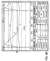
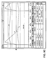
- Figures 8A-D and 9A-C show exemplary simulations which illustrate operation in damped reverse boost mode.
- circuit values are chosen as follows: Veq 15V L2e 30nH C .44uH L 7.5uH Co 400uF Ro 12.5mOhm Vout 5v where L2e is the secondary-referenced equivalent leakage inductance of the leakage inductance transformer 14 of Figure 7, and Veq is, as noted earlier, approximately equal to Vin*(N2/N1).
- Figures 9A-C show similar waveforms for Vc, Io, and Vc o at an operating frequency of 200 kHz for values of Rd equal to 4, 2 and 0 ohms, respectively.
- the value in the "VALUE” column for channel 3 (corresponding to the output current) reflects the average output current delivered to the load.
- the value in the "VALUE” column for channel 4 reflects the power dissipated in the damping resistor Rd.
- Rd near the critically damped value such that ripple voltage is reduced to some desired value, or such that minimum operating frequency is raised to some desired value, but where dissipation is not deemed to be excessive. It is to be noted, however, that dissipation in Rd occurs only at relatively low values of load where the loss in Rd is usually more than offset by reduced losses in the remainder of the converter circuitry. As discussed below, at higher loads, where current reversal in the output inductor does not occur, and where overall converter loss associated with increased forward power processing is increased, dissipation in Rd will be reduced essentially to zero.
- both the capacitor voltage, Vc (labeled E), and the reverse inductor current, Iout, (labeled B) can be seen to rise smoothly, without overshoot, towards their peak values.
- the rate of rise of reverse current in the slightly overdamped case ( Figure 8C) is seen to be slower than the rate of rise with critical damping ( Figure 8B).
- Vc and Iout are seen to overshoot slightly as they converge toward final values.
- Figs. 9A-C illustrate that the boost switch has essentially no effect at higher frequencies. This is because at higher frequencies the output current Iout never reverses and the bulk of the forward current flowing in the output inductor will be bypassed around the second switching device and damping resistor by the second unidirectional conducting device.
- the damping resistor 210 shown in Figure 7 need not be a fixed resistor, but can be any dissipative element of appropriate value.
- the damping resistor might be a PTC thermistor (positive temperature coefficient thermistor).
- PTC thermistor positive temperature coefficient thermistor
- Such a device has a relatively stable value of resistance until it reaches a specified operating temperature, at which point its resistance increases sharply.
- One benefit of using a PTC thermistor is that potentially troublesome side effects of certain faults in arrays of driver and booster (see Vinciarelli, U.S. Patent No. 4,468,020, the disclosure of which is to be regarded as effectively incorporated herein by reference) converters which incorporate damped reverse boost may be avoided.
- the second switching device 252 of Figure 7 might be a unidirectional switch (e.g. a field effect transistor 260, as illustrated in the Figure 10A, or a bipolar transistor 270, as shown in Figure 10B).
- the unidirectional switch 260, 270 would be oriented relative to the second unidirectional conducting device 250 so that they would respectively conduct current in opposite directions.
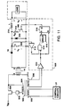
- control circuits 22 turn the first switch 526 on and off, at times of zero current, at an operating frequency consistent with maintaining the output voltage of the converter at an essentially fixed value Vo.
- the first switch which, in the Figure, is shown to be a field effect transistor, is turned on and off via a coupling transformer 500 and gate interface circuitry 505.
- the first switch is turned on when the control circuits send a first signal (e.g. a positive going edge) to the primary winding 502 of the coupling transformer 500.
- the interface circuits 505 sense this signal via secondary winding 504 and turn on the first switch.
- the turn-on signal is also routed to a first comparator 510, included in controller circuitry 508, which delivers a high-going signal to gate 514 when it senses the presence of the turn-on signal.
- Second comparator 512 is arranged to deliver a high-going output to gate 514 when the capacitor voltage is at a value essentially equal to zero volts.
- the gate 514 output will go high when the second comparator output goes high, provided that the output of the first comparator is not high (as indicated by the circular negation symbol at the input of the gate which is connected to the output of the first comparator).
- the Q output of the flip-flop will go high, and turn the second switching device on, when the S input to the flip-flop is driven momentarily high; it will go low, turning the second switching device off, when the R input to the flip-flop is driven momentarily high. Therefore, when the control circuits deliver a turn-on signal to the first switch 526, and the output of the first comparator goes high, the R input of the flip-flop will be driven high and the S input will be driven low, causing the second switching device to be turned off. In the event that the signal delivered by the first comparator 510 lasts only momentarily, and the converter is running at a relatively high value of load, there may a short delay between the first switch being closed and the capacitor voltage rising above zero volts.
- control circuits for opening and closing the first switching device at zero current and controlling the rate at which the switch is opened and closed as a means of maintaining the converter output voltage, Vout, at some desired setpoint value. Details of one means of implementing such control circuits are illustrated in Figure 12, which shows a portion of a zero-current switching converter consisting of switch controller 441, a first switching device 440, a current transformer 400 connected in series with the first switching device 440, an error amplifier 490, a variable frequency pulse generator 500, and a voltage divider 495.
- Figure 12 shows a portion of a zero-current switching converter consisting of switch controller 441, a first switching device 440, a current transformer 400 connected in series with the first switching device 440, an error amplifier 490, a variable frequency pulse generator 500, and a voltage divider 495.
- a fraction of the converter output voltage, V1 K ⁇ Vout , is supplied to an input of the error amplifier 490 by the voltage divider 495.
- a reference voltage, Vref indicative of some desired value of converter output voltage, is delivered to the other input of the error amplifier. If the signal V1 is greater than Vref, the output of the error amplifier will decrease; if the signal V1 is less than Vref, the output of the error amplifier will increase.
- the output of the error amplifier is delivered to a variable frequency pulse generator 497. As the error amplifier output increases, the frequency of the pulse train signal, Vf, delivered to the switch controller 441, will increase, thereby increasing the rate at which converter operating cycles are initiated (i.e. increasing the converter operating frequency).
- the pulses delivered by the pulse generator 497 are delivered to the S input of the flip-flop 470.
- the output of the flip-flop,VQ goes high when a high signal is applied to the S input and goes low when a high signal is applied to the R input.
- the signal VQ goes high.
- the signal VQ is delivered to a switch driver 410 which closes the first switching device 440 when VQ is high.
- the switch driver might include the transformer 500 and gate interface circuitry 505 of Figure 11.
- switch current Isw
- switch current Isw
- a fraction of this current flows in the signal diode 430 connected to the secondary of the current transformer 400 (the turns ratio, N2/N1, being greater than one).
- the diode voltage, VI is delivered to one input of the comparator 480.
- a threshold voltage, Vt (for example, 0.1 V), is delivered to the other input of the comparator.
- Vt for example, 0.1 V
- the switch controller 441 of Figure 12 is arranged so that it opens the switch at essentially the first instant in time, following the time when the switch is turned on, when the current returns to zero.
- the presence of the second unidirectional conducting device 18 constrains the average value of I2 to positive values which flow in the direction of conduction of the second unidirectional conducting device 18. Since both I1 and I2 are constrained to be positive then equation 2 requires: Iout/I1 ⁇ 1 Since, from Equation 1: Veq ⁇ Vout*Iout/I1 then Veq ⁇ Vout . In the topology of Figure 1B, by constraining the average current I2 to a range of positive values only, the behavior of the second unidirectional conducting device 18 forces the converter to operate in a "buck" mode.
- closure of the first switching device 26 impresses the transformed input source voltage Veq across the effective inductance 114, whose initial instantaneous current, I1, is zero.
- a positive ramp of current I1 will flow in the effective inductance 114 until the current in the second unidirectional conducting device 18 (i.e., the difference between the instantaneous current in the effective inductance 114 and the instantaneous current in the second inductor 24, Iout), becomes zero, at which time the second unidirectional conducting device 18 ceases conducting.
- the second unidirectional conducting device 18 ceases conducting, energy transfer from the transformed input source via the effective inductance 114 to the capacitor 20 and load commences. It can be shown that during this energy transfer cycle the voltage across the capacitor 20 will be: and the current in the effective inductance 114 is: where:
- the second unidirectional conducting device 18 ceases conducting when the values of I1 and Iout are equal.
- the values of Ip and Io are also equal, and Equations 4 and 4a reduce to:
- FIG. 1 A schematic diagram illustrating an alternate embodiment of typical commercially available single switching devices cannot efficiently perform the function of the bidirectional second switch 28, in Figure 2, at the high operating frequencies at which the converter will operate.
- An alternate embodiment replaces the second switch 28, of Figure 2, with the circuit arrangement of Figure 3.
- the circuit is comprised of a second unidirectional conducting device 50 connected across a unidirectional switch 52, such that the preferred directions of conduction of the two devices are in opposition (as indicated by the arrows adjacent to the two devices).
- the unidirectional switch 52 might be a bipolar or a MOSFET transistor.
- the current flowing in the effective inductance 114 during the forward energy transfer phase can be shown to be: Examination of Equation 10 reveals that both the peak value of I1(t), and the time duration during which I1(t) is positive (i.e., the time period t0 to t1), are strongly dependent on the value, Ix, of negative current Iout which is flowing at time t0. This is to be expected, since, after opening the second switch 28, the negative current Ix starts to positively charge the capacitor 20. Positive voltage buildup on the capacitor 20, in response to the negative current Ix, acts to reduce the voltage across the effective inductance 114 during the energy transfer phase, thereby acting as a barrier to current flow and reducing forward energy transfer.
- Figure 5 shows waveforms of the forward current, I1(t), of Equation 11, for different values of the ratio Ir/If.
- the effect of increasing the ratio Ir/If i.e., increasing Ix
- Equation 11 Mathematical integration of Equation 11, over the time period during which positive current flows, results in a value for the amount of charge transferred per cycle, Q.
- Figure 6 shows the effect of reverse current, Ix, on forward charge transferred per cycle fcr a converter operating in reverse boost mode.
- Figures 5 and 6 illustrate the effect that initial reverse current flow in the second inductor 24 has upon forward energy transfer per cycle.
- the effect of initial reverse current flow in the second inductor 24 is a reduction in forward energy transferred during the cycle. Since Ix will become more negative as the average value of load current, Iout, drops, the amount of charge transferred per cycle will also drop. The result is that, for a given value of load, and all other circuit elements being equal in value, a converter operating in reverse boost mode must operate at a higher frequency than a prior art converter.
- the converter of Figures 2A-B When operated in reverse boost mode, the converter of Figures 2A-B can operate down to no load without the deleterious effects of "discontinuous" mode.
- reverse boost eliminates the source of discontinuous mode while at the same time reducing the relative range of frequencies over which the converter will operate as load is decreased.
- reducing the inductance value of the second inductor 24 is not only made possible by reverse boost, it is required to ensure that current reversal will occur at light loads.
- the second switching device 28 in the converter is implemented using the topology of Figure 3.
- a MOSFET transistor with an on-resistance of approximately 30 milliohms is used for switch 52, and a Schottky diode is used for the unidirectional conducting device 50.
- the value, L, of the second inductor 24 is 10 microhenries, while in the converter operating in reverse boost mode, the inductance value is reduced to 3 microhenries.
- the discontinuous mode is eliminated since the second switching device 28 prevents reverse energy transfer between the second inductor 24 and the capacitor 20.
- operation at an average output current of 1 Ampere occurs at a stable converter operating frequency of about 161 Kilohertz. This is higher than the operating frequency of the prior art converter operating at the same load because the value of the second inductor 24 has been reduced, and current reversal in the second inductor (at a value Ix of about 1.8 Amperes) is occurring in the present converter at this value of load, resulting in a reduction of forward energy transferred per cycle.
- reverse boost would be implemented by using the circuit of Figure 3 as the second switch 28 in the converter of Figure 2A.
- the value of second inductor 24 would be reduced relative to a prior art converter.
- the controller 32 would open the unidirectional switch 52 at essentially the same time that the first switch 26 was closed, and close the unidirectional switch 52 when the capacitor 20 voltage returned to zero.
- the variable frequency control circuit of the prior art converter would be used as the control circuit 22 for the first switch. At relatively high loads, the operating frequency would be relatively high, and the current in the second inductor 24 would always flow in a positive direction.
- Reverse boost will become a self-regulating process in that the converter operating frequency will stabilize at a value such that the reverse current in the second inductor 24 at the start of a cycle (Ix of Equation 10) is sufficient to maintain the output voltage in regulation at the particular value of load.
- the lower limit on operating frequency in the reverse boost mode of operation will effectively be dependent upon the small amount of losses present in the circuit elements forming the output circuit.
- a value of Ix will be reached at which forward power flow will just be sufficient to compensate for output circuit losses.
- the topology of Figure 2A may be used to selectively regulate the amount of forward energy transferred during a converter operating cycle, while simultaneously regulating reverse energy transfer from energy storing elements in the load to the capacitor 20. Elimination of the "discontinuous" operating mode at low values of load, and reduction in the range of frequencies over which the converter operates as load is reduced, are two of the resulting benefits.
- an appropriate controller 32 which may be a part of control circuit 22
- many possible converter operating modes can be realized which exploit this mechanism.
- reverse boost might be used solely to eliminate the discontinuous mode at light loads while raising the minimum converter operating frequency.
Landscapes
- Engineering & Computer Science (AREA)
- Power Engineering (AREA)
- Dc-Dc Converters (AREA)
Applications Claiming Priority (2)
| Application Number | Priority Date | Filing Date | Title |
|---|---|---|---|
| US862490 | 1992-04-02 | ||
| US07/862,490 US5291385A (en) | 1992-04-02 | 1992-04-02 | Zero-current switching forward power converter operating in damped reverse boost mode |
Publications (3)
| Publication Number | Publication Date |
|---|---|
| EP0564289A2 EP0564289A2 (en) | 1993-10-06 |
| EP0564289A3 EP0564289A3 (OSRAM) | 1994-04-20 |
| EP0564289B1 true EP0564289B1 (en) | 1997-07-23 |
Family
ID=25338620
Family Applications (1)
| Application Number | Title | Priority Date | Filing Date |
|---|---|---|---|
| EP93302584A Expired - Lifetime EP0564289B1 (en) | 1992-04-02 | 1993-04-01 | Zero-current switching forward converter |
Country Status (4)
| Country | Link |
|---|---|
| US (1) | US5291385A (OSRAM) |
| EP (1) | EP0564289B1 (OSRAM) |
| JP (1) | JP2576012B2 (OSRAM) |
| DE (1) | DE69312364T2 (OSRAM) |
Families Citing this family (17)
| Publication number | Priority date | Publication date | Assignee | Title |
|---|---|---|---|---|
| JP2868422B2 (ja) * | 1993-10-28 | 1999-03-10 | ヴィエルティー コーポレーション | 電力変換における電流検出装置及び方法 |
| US5623397A (en) * | 1994-01-27 | 1997-04-22 | Vlt Corporation | Power conversion in anticipatory reverse boost mode |
| EP0881758B1 (en) * | 1994-04-08 | 2004-06-23 | Vlt Corporation | Efficient power conversion |
| US5838557A (en) * | 1997-07-28 | 1998-11-17 | Altor, Inc. | Circuit for use in a DC-DC converter having a booster module |
| US6493678B1 (en) * | 1998-05-22 | 2002-12-10 | Connectrix Systems, Inc. | Method, apparatus and system for merchandising related applications |
| US6038147A (en) * | 1998-11-12 | 2000-03-14 | Lucent Technologies Inc. | Power supply employing circulating capacitor and method of operation thereof |
| KR100344532B1 (ko) * | 2000-07-31 | 2002-07-24 | 삼성전자 주식회사 | 휴대용 컴퓨터용 에이씨/디씨 어댑터의 절전회로 |
| US6680809B1 (en) | 2000-10-12 | 2004-01-20 | International Business Machines Corporation | Write head current damping with dynamic coupling |
| US7204683B2 (en) | 2001-06-22 | 2007-04-17 | The Furukawa Electric Co., Ltd. | Molding die for covering optical fiber and optical fiber cover forming device |
| JP4386133B2 (ja) * | 2005-02-15 | 2009-12-16 | 株式会社村田製作所 | 電源装置 |
| JP2007020305A (ja) * | 2005-07-07 | 2007-01-25 | Toshiba Corp | パルス電源装置 |
| GB2447873B (en) * | 2007-03-30 | 2009-07-29 | Cambridge Semiconductor Ltd | Forward power converter controllers |
| GB2448117B (en) * | 2007-03-30 | 2009-06-03 | Cambridge Semiconductor Ltd | Forward power converter controllers |
| GB2447874B (en) * | 2007-03-30 | 2009-07-29 | Cambridge Semiconductor Ltd | Forward power converter controllers |
| US9263967B2 (en) * | 2010-07-22 | 2016-02-16 | Earl W. McCune | AC/DC power conversion methods and apparatus |
| KR101288206B1 (ko) * | 2011-02-08 | 2013-07-18 | 명지대학교 산학협력단 | 하이브리드 스위칭 구조를 가지는 전력 변환기 |
| US9219369B2 (en) * | 2013-03-15 | 2015-12-22 | Qualcomm Incorporated | Multiphase charger |
Family Cites Families (7)
| Publication number | Priority date | Publication date | Assignee | Title |
|---|---|---|---|---|
| US4415959A (en) * | 1981-03-20 | 1983-11-15 | Vicor Corporation | Forward converter switching at zero current |
| FR2608857B1 (fr) * | 1986-12-19 | 1989-05-12 | Sodilec Sa | Convertisseur continu-continu du type " forward " a commutation a courant nul et a fonctionnement en courants bidirectionnels |
| FR2632134B1 (fr) * | 1988-05-26 | 1990-09-14 | Cachan Lesir Ecole Normale Sup | Procede de linearisation pour convertisseur continu-continu et dispositifs mettant en oeuvre ce procede |
| US4831507A (en) * | 1988-09-12 | 1989-05-16 | Reliance Comm/Tec Corporation | Frequency controlled preload |
| US5235502A (en) * | 1989-11-22 | 1993-08-10 | Vlt Corporation | Zero current switching forward power conversion apparatus and method with controllable energy transfer |
| CA2029209C (en) * | 1989-11-22 | 1999-07-27 | Patrizio Vinciarelli | Zero-current switching forward power conversion with controllable energy transfer |
| US5003451A (en) * | 1989-12-21 | 1991-03-26 | At&T Bell Laboratories | Switched damper circuit for dc to dc power converters |
-
1992
- 1992-04-02 US US07/862,490 patent/US5291385A/en not_active Expired - Lifetime
-
1993
- 1993-04-01 JP JP5075453A patent/JP2576012B2/ja not_active Expired - Fee Related
- 1993-04-01 EP EP93302584A patent/EP0564289B1/en not_active Expired - Lifetime
- 1993-04-01 DE DE69312364T patent/DE69312364T2/de not_active Expired - Fee Related
Also Published As
| Publication number | Publication date |
|---|---|
| JP2576012B2 (ja) | 1997-01-29 |
| DE69312364D1 (de) | 1997-09-04 |
| EP0564289A3 (OSRAM) | 1994-04-20 |
| DE69312364T2 (de) | 1998-02-26 |
| JPH0654530A (ja) | 1994-02-25 |
| EP0564289A2 (en) | 1993-10-06 |
| US5291385A (en) | 1994-03-01 |
Similar Documents
| Publication | Publication Date | Title |
|---|---|---|
| EP0564289B1 (en) | Zero-current switching forward converter | |
| US5321348A (en) | Boost switching power conversion | |
| US8437154B2 (en) | Method and apparatus for varying a duty cycle of a power supply controller responsive to multiple linear functions over a range of values of a feedforward signal | |
| US7154250B2 (en) | Buck-boost DC—DC switching power conversion | |
| US5912552A (en) | DC to DC converter with high efficiency for light loads | |
| US5335162A (en) | Primary side controller for regulated power converters | |
| US5751139A (en) | Multiplexing power converter | |
| EP0074399B1 (en) | Forward converter switching at zero current | |
| US9166481B1 (en) | Digital control of resonant power converters | |
| EP0744817B1 (en) | Reverse energy transfer in zero-current switching power conversion | |
| US5731731A (en) | High efficiency switching regulator with adaptive drive output circuit | |
| US5880940A (en) | Low cost high efficiency power converter | |
| EP0262812B1 (en) | Buck-boost parallel resonant converter | |
| US10050519B2 (en) | Control of buck-boost power converter with input voltage tracking | |
| US5235502A (en) | Zero current switching forward power conversion apparatus and method with controllable energy transfer | |
| US20030095421A1 (en) | Power factor correction circuit | |
| US5623397A (en) | Power conversion in anticipatory reverse boost mode | |
| EP1503489B1 (en) | System and method to limit maximum duty cycle | |
| EP0429310B1 (en) | Zero-current switching forward power conversion | |
| US12483138B1 (en) | High-bandwidth factorized power system and regulator |
Legal Events
| Date | Code | Title | Description |
|---|---|---|---|
| PUAI | Public reference made under article 153(3) epc to a published international application that has entered the european phase |
Free format text: ORIGINAL CODE: 0009012 |
|
| AK | Designated contracting states |
Kind code of ref document: A2 Designated state(s): DE FR GB |
|
| PUAL | Search report despatched |
Free format text: ORIGINAL CODE: 0009013 |
|
| AK | Designated contracting states |
Kind code of ref document: A3 Designated state(s): DE FR GB |
|
| 17P | Request for examination filed |
Effective date: 19940511 |
|
| 17Q | First examination report despatched |
Effective date: 19950929 |
|
| GRAG | Despatch of communication of intention to grant |
Free format text: ORIGINAL CODE: EPIDOS AGRA |
|
| GRAH | Despatch of communication of intention to grant a patent |
Free format text: ORIGINAL CODE: EPIDOS IGRA |
|
| GRAH | Despatch of communication of intention to grant a patent |
Free format text: ORIGINAL CODE: EPIDOS IGRA |
|
| GRAA | (expected) grant |
Free format text: ORIGINAL CODE: 0009210 |
|
| AK | Designated contracting states |
Kind code of ref document: B1 Designated state(s): DE FR GB |
|
| REF | Corresponds to: |
Ref document number: 69312364 Country of ref document: DE Date of ref document: 19970904 |
|
| ET | Fr: translation filed | ||
| PLBE | No opposition filed within time limit |
Free format text: ORIGINAL CODE: 0009261 |
|
| STAA | Information on the status of an ep patent application or granted ep patent |
Free format text: STATUS: NO OPPOSITION FILED WITHIN TIME LIMIT |
|
| 26N | No opposition filed | ||
| REG | Reference to a national code |
Ref country code: GB Ref legal event code: IF02 |
|
| PGFP | Annual fee paid to national office [announced via postgrant information from national office to epo] |
Ref country code: GB Payment date: 20050323 Year of fee payment: 13 |
|
| PGFP | Annual fee paid to national office [announced via postgrant information from national office to epo] |
Ref country code: FR Payment date: 20050418 Year of fee payment: 13 |
|
| PGFP | Annual fee paid to national office [announced via postgrant information from national office to epo] |
Ref country code: DE Payment date: 20050531 Year of fee payment: 13 |
|
| PG25 | Lapsed in a contracting state [announced via postgrant information from national office to epo] |
Ref country code: GB Free format text: LAPSE BECAUSE OF NON-PAYMENT OF DUE FEES Effective date: 20060401 |
|
| PG25 | Lapsed in a contracting state [announced via postgrant information from national office to epo] |
Ref country code: DE Free format text: LAPSE BECAUSE OF NON-PAYMENT OF DUE FEES Effective date: 20061101 |
|
| GBPC | Gb: european patent ceased through non-payment of renewal fee |
Effective date: 20060401 |
|
| REG | Reference to a national code |
Ref country code: FR Ref legal event code: ST Effective date: 20061230 |
|
| PG25 | Lapsed in a contracting state [announced via postgrant information from national office to epo] |
Ref country code: FR Free format text: LAPSE BECAUSE OF NON-PAYMENT OF DUE FEES Effective date: 20060502 |