EP0563877B1 - Color signal clipping or limiting apparatus - Google Patents
Color signal clipping or limiting apparatus Download PDFInfo
- Publication number
- EP0563877B1 EP0563877B1 EP93105236A EP93105236A EP0563877B1 EP 0563877 B1 EP0563877 B1 EP 0563877B1 EP 93105236 A EP93105236 A EP 93105236A EP 93105236 A EP93105236 A EP 93105236A EP 0563877 B1 EP0563877 B1 EP 0563877B1
- Authority
- EP
- European Patent Office
- Prior art keywords
- signal
- color video
- state
- video signal
- color
- Prior art date
- Legal status (The legal status is an assumption and is not a legal conclusion. Google has not performed a legal analysis and makes no representation as to the accuracy of the status listed.)
- Expired - Lifetime
Links
Images


Classifications
-
- H—ELECTRICITY
- H04—ELECTRIC COMMUNICATION TECHNIQUE
- H04N—PICTORIAL COMMUNICATION, e.g. TELEVISION
- H04N9/00—Details of colour television systems
- H04N9/64—Circuits for processing colour signals
- H04N9/68—Circuits for processing colour signals for controlling the amplitude of colour signals, e.g. automatic chroma control circuits
Definitions
- This invention concerns apparatus for limiting the amplitude of color signals in a color television camera or a color television signal processor.
- it relates to apparatus for detecting when the amplitude of one color signal has been limited in order to limit the amplitude of other color signals.
- One step in the alignment of a television camera is to obtain proper color balance. This is performed by placing a white object in the field of view of the camera and either manually adjusting the gains of the various red, green and blue color signals or allowing the camera to automatically adjust the gains of the color signals to produce signal which will cause a white image of the object to be reproduced on a display device.
- the color signal levels produced by the color balance operation define maximum red, green and blue signal levels for the camera.
- a problem may occur, however, when, after color balance calibration, an image viewed by the camera contains objects which are brighter than the object that was used for the color balance operation or which have higher color saturation values than are allowed by the respective red, green and blue signal levels developed from the color balance operation.
- the respective red, green and blue signals which describe these objects may be clipped. That is to say, held at the maximum digital or analog value that may be provided by the camera.
- Color signal clipping is described in this reference as a type of distortion which can be detected but not corrected.
- Two solutions to this problem are proposed. First, to eliminate the effective pixels from further consideration and, second, to make educated guesses as to what the true hue of the distorted pixels may be. The paper gives no guidance as to how these educated guesses might be made.
- the present invention is embodied in a color video signal processing system which determines when one color signal has been clipped and, in response to this determination, acts to limit the amplitude of the other color signals to an amplitude value exhibited by each color video signal at the time the clipped signal was detected so as to maintain accurate hue information in the reproduced image.
- the other color signals are held at amplitude values which occurred at the instant the clipped signal was detected.
- the amplification factor applied to the other color signals is limited to reduce the amplitude of the unclipped signals without eliminating amplitude variations.
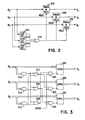
- Figure 1 is a block diagram of an exemplary color television camera which includes an embodiment of the present invention.
- FIG 2 is a block diagram of a color limiting and clipping apparatus suitable for use in the camera shown in Figure 1.
- Figure 3 is a logic diagram showing an exemplary color limiting and clipping circuit which may be used in a digital camera system.
- Figure 4 is a block diagram of an exemplary color-signal gain-limiting apparatus suitable for use as the color-clipping/limiting circuit shown in Figure 1.
- FIG 5 is a logic diagram showing digital color-signal gain-limiting apparatus which may be used as the color-clipping/limiting circuitry in the camera shown in Figure 1.
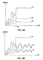
- Figures 6A and 6B are graphs of signal amplitude versus time which are useful for describing the operation of the circuitry shown in Figures 1 through 5.
- a CCD imager 110 provides red (R), green (G) and blue (B) signals representing a color image.
- the CCD imager 110 may include, for example, a conventional CCD matrix having an integral color filter mosaic and circuitry which processes the signals provided by the CCD matrix to generate separate red, green and blue color signal components.
- the analog red, green and blue signals provided by the CCD imager 110 are applied to analog-to-digital converter (ADC) 112 which generates respective digitally sampled red R', green G' and blue B' color signals synchronous with a clock signal, CLOCK, provided by a clock signal generator 111.
- ADC analog-to-digital converter
- the digitized color signals provided by the ADC 112 are applied to color-balance circuitry 114. Circuitry 114 automatically adjusts amplification factors applied to the respective digital signals so that the brightest object in the camera's field of view will appear white on the reproduced image.
- the color-balance calibration is performed once during the initial camera set-up.
- the gain factors developed in this calibration step are applied to the R', G' and B' signals provided by the ADC 112 during the remainder of normal imaging operation. If a signal exceeds the maximum amplitude value which can be represented by a digital signal value, for example, 255 for an 8-bit digital sample, the color-balance circuit 114 limits the value of that signal to the maximum digital value.
- Amplitude-adjusted red, green and blue color signals (R b , G b , and B b ) provided by the color-balance circuitry 114 are applied to a color clip/limit circuit 116.
- the circuit 116 is described in detail below with reference to figures 2 through 6.
- Red, green and blue color signals (R o , G o and B o ) provided by the color clip/limit circuit are applied in parallel to color correction circuitry 118 and aperture signal generator 124.
- the color correction circuitry 118 may, for example, process the color signals R o , G o and B o provided by the circuitry 116 to generate color-shifted red, green and blue signals which produce correct image hues on a target image device.
- the circuitry 118 effectively converts the colors passed by the color filters used in the CCD imager 110 into signals which will reproduce the image colors correctly under a target video standard (e.g. NTSC, PAL or SECAM).
- a target video standard e.g. NTSC, PAL or SECAM
- the corrected color signals provided by the circuitry 118 are applied to gamma correction circuitry 120.
- Gamma correction circuitry 120 applies a non-linear transfer function to the corrected red, green and blue color signals produced by the circuitry 118 to provide signals which generate proper gray-scale images under a target video standard (e.g. NTSC, PAL or SECAM).
- a target video standard e.g. NTSC, PAL or SECAM.
- the output signals provided by the gamma correction circuitry 120 are delayed through a delay element 122, which compensates for signal processing delays through the aperture signal generator 124, and are then applied to respective adders 126, 128 and 130.
- the other input signal to each of the adders 126, 128 and 130 is a peaking signal generated by the aperture signal generator 124.
- This peaking signal is a high-frequency signal which is added to all of the component color signals.
- the effect of this operation is to emphasize high-frequency components in the image signal relative to low-frequency components. Since this signal is added to each of the red, green and blue color signals, it acts to emphasize the high-frequency components as a monochrome signal. That is to say, the effect it produces is visible mainly in the luminance signal, Y, produced by the camera.
- the output signals (R'',G'' and B'') of the adders 126, 128 and 130 are applied to a matrix 32 which generates the luminance signal, Y, and two color difference signals, I and Q, from the three primary color signals R'', G'' and B''.
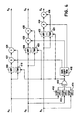
- FIG 2 is a block diagram of exemplary clip/limit circuitry which may be used as the circuitry 116 shown in Figure 1.
- the circuitry shown in Figure 2 operates on analog red, green and blue signals. Accordingly, if this circuitry were used in the camera shown in Figure 1, ADC 112 would be omitted and at least the color balance circuitry 114 would operate on analog signal levels.
- the signals R b , G b and B b are applied to respective track-and-hold circuits 218, 220 and 222.
- Each of these circuits may include, for example, a capacitive storage element (not shown) coupled to receive the respective color signal through an analog gate (not shown).
- the track-and-hold circuits are controlled by a signal HOLD provided by an OR gate 216. In the exemplary circuit, this signal controls the conductivity of the analog gate.
- the output signal of the track-and-hold circuit will either track the signal applied to the circuit (analog gate conductive) or hold it at the signal level applied to the circuit when the signal HOLD was activated (analog gate non-conductive).
- the OR gate 216 receives three input signals from respective clip detection circuits 210, 212 and 214.
- the clip detection circuit 210 is coupled to receive the red color signal (R b ) while the circuits 212 and 214 are coupled to receive the green G b and blue B b color signals respectively.
- the clip detection circuits 210, 212 and 214 may be, for example, conventional threshold detectors which detect when one of the red, green and blue color signals exceed a predetermined threshold value. When this occurs, the detecting circuit emits a logic-high level. When any one of the circuits 210, 212 and 214 emits a logic-high level, the signal HOLD applied to all three track-and-hold circuits 218, 220 and 222 becomes logic-high. In response to a logic-high value for the signal HOLD, the track-and-hold circuits 218, 220 and 222 maintain their respective output signal levels at the values they passed when the signal HOLD became logic-high.
- FIG. 6A The effect of this circuit is shown in Figure 6A.
- the signal R exceeds the threshold value and is detected by the clip detector 210.
- the clip detector 210 applies a logic-high value to the OR gate 216.
- the gate 216 applies the signal HOLD to the three track-and-hold circuits 218, 220 and 222.
- This signal causes the track-and-hold circuits 220 and 222 to maintain the level of the respective green and blue signals at the level which occurred at time T 1 , the time that the clipped R b signal was detected. These levels are maintained until the level of the signal R b which initiated the limit operation falls below the threshold at time T 2 .
- the track-and-hold circuits 218, 220 and 222 follow the variations of the respective signals R b , G b and B b .
- the track-and-hold circuits 220 and 222 hold the respective signals G o and B o at the respective values of G b and B b at time T 3 .
- Figure 3 is a logic diagram of a digital circuit which operates in the same manner as the circuit shown in Figure 2.
- the red, green and blue color signals are applied to respective AND gates 310, 312 and 313.
- These AND gates act as digital value decoders. When all of the input signals to one of these gates are logic-high, the respective color signal value is the largest digital value that can be represented and, so, the output signal of the gate is logic-high.
- the output signals produced by AND gate 310 are applied to first input terminals of NOR gates 314 and 316, respectively.
- the output signal of AND gate 312 is applied to NOR gates 316 and 318 while the output signal of AND gate 313 is applied to NOR gates 318 and 314.
- the output signal of NOR gate 314 is applied to one input terminal of an AND gate 322 while the output signal of NOR gate 316 is applied to one terminal of AND 324 and the output signal of NOR gate 318 is applied to one input terminal of an AND gate 320.
- the other input terminal of each of the AND gates 320, 322 and 324 is coupled to receive the clock signal CLOCK.
- the output terminals of the AND gates 320, 322 and 324 are coupled to respective clock input terminals of latches 326, 328 and 330.
- the data input terminals of these latches are coupled to receive the respective R b , G b and B b color signals.
- the output signals of the latches 326, 328 and 330 are the respective limited R o , G o and B o color signals.
- the red, green and blue color signals are latched, one sample at a time responsive to the signal CLOCK, into latches 326 and 328 and 330. These samples are available at the output ports of the respective latches with a delay of one period of the sampling clock signal CLOCK.
- the respective clip detector 310, 312 or 313 When one of the signals R b , G b or B b has a value of all ones (e.g. 255 for an 8-bit sample), the respective clip detector 310, 312 or 313 will provide a logic high output signal to two of the NOR gates 314, 316 and 318. In response to this signal, the NOR gates will provide logic-low output signals, disabling two of three latches from changing state. Thus, these latches will hold the corresponding signal levels of the other two color signals to respective levels which occurred at the time that the one color signal was detected as being clipped.
- the circuitry shown in Figure 4 operates on analog R b , G b and B b color signals.
- the clip detectors 410, 412 and 414 and the OR gate 416 operate in the same manner as the respective elements 210, 212, 214 and 216 shown in Figure 2.
- the output signal of the OR gate 416 is applied to a gain coefficient ROM 418 and to control input terminals of three track and hold circuits 419, 425 and 431.
- the ROM 418 provides a digital control signal to each of three two-quadrant multipliers 420, 422 and 424.
- the track-and-hold circuits 419, 425 and 431 are coupled to receive respective color signals R b , G b and B b . Unlike the embodiment shown in Figure 2, however, these color signals are also coupled to respective high-pass filters 420, 426 and 432. The output signals provided by these filters are applied to the multipliers 422, 428 and 434, respectively.
- the scaled high-frequency components of the signals R b , G b and B b provided by the multipliers 422, 428 and 434 are, in turn, added to the respective output signals of the track-and-hold circuits 419, 425 and 431 by the adders 424, 430 and 436 to produce the signals R o , G o and B o , respectively.
- the circuit shown in Figure 4 superimposes attenuated high-frequency components of the various color signals onto the signals produced by the track-and-hold circuits when any one clipped color signal is detected.
- the gain coefficient ROM 418 provides a factor of zero to the multipliers 422, 428 and 434 so the output signals R o , G o and B o are the signals R b , G b and B b passed by the respective track-and-hold circuits 419, 425 and 431.
- the multipliers 422, 428 and 434 may be eliminated in the circuit shown in Figure 4 if a low-pass filter (not shown) is inserted before each of the track and hold circuits 419, 425 and 431.
- the high-pass filters 420, 426 and 432 pass the high frequency components of the signals with a gain of unity while the track and hold circuits 419, 425 and 531 track or hold only the low-frequency components of the signals.
- the signals provided by the respective high-pass filters and track and hold circuits are summed in the adders 424, 430 and 436 to produce the output signals R o , G o and B o .
- Figure 5 is a logic diagram of digital circuitry which performs substantially the same function as the circuitry shown in Figure 4.
- clip detectors 510, 512 and 514 are coupled to receive the R b , G b and B b signals respectively and to provide a logic-high output signal when one of the color signals has been clipped.
- the output signals of these detectors are ORed by the orgate 516 to produce a single control signal which is applied to each of three track and hold circuits 518, 520 and 522.
- These clip detectors and track and hold circuits operate in the same manner as the gates 310, 312 and 313, and latches 326, 328 and 330, described above.
- the output signals of the track and hold circuits 518, 520 and 522 are coupled to first input ports of respective magnitude comparators 524, 526 and 528.
- the second input port of each of the magnitude comparators 524, 526 and 528 are coupled to receive the respective signals R b , G b and B b .
- the signals R b , G b and B b are also applied to respective gain control circuits 530, 532 and 534 which are controlled by output signals generated by the magnitude comparators 524, 526 and 528, respectively.
- the gain control circuits 530, 532 and 534 may be, for example; read-only memories (ROM's) which pass the signals R b , G b and B b as the signals R o , G o and B o when the output signal of the respective magnitude comparators are logic-low and pass an attenuated version of the respective signals R b , G b and B b otherwise.
- ROM's read-only memories
- These read-only memories may be configured as linear or non-linear multipliers.
- the invention is described in terms of the red color signals R b and R o .
- the same analysis applies for the green color signals G b and G o and the blue color signals B b and B o .
- the 8-bit signal R b is applied as the 8 least-significant bits (LSB's) of the address value applied to gain control circuitry 530.
- the output signal of the magnitude comparator 524 is applied as the most significant bit (MS) of the address value.
- MSB of the address value is zero and the 256 values which define the range of the R b signal are passed without translation as the output signal R o .
- the track and hold circuit 518 When one of the signals G b or B b is clipped, however, the track and hold circuit 518 is engaged to hold the red signal at the value of R b which occurred when the clipped G b or B b signal was detected. If the instantaneous level of the signal R b exceeds this held value, output signal of the magnitude detector 524 becomes logic-high, changing the range of address values applied to the gain control circuitry 530. In response to this changed address range, the circuitry 530 passes an attenuated version of the signal R b as the signal R o .
- Gain control circuits 532 and 534 are similarly configured to accept the respective G b and B b signals as the 8 LSB's. Circuit 532 is configured to accept the output signal of magnitude comparator 526 as the most significant address bit while circuit 534 is configured to accept the output signal of magnitude comparator 528 as the most significant address bit. In this configuration, each of the signals R b , G b and B b may be scaled by a respectively different attenuation function responsive to clipping in any of the other color signals.
- Figure 6B is a graph of signal amplitude versus time for each of the red, green and blue color signals which illustrates the operation of the circuits shown in Figures 4 and 5 when the red signal is clipped.
- the dashed lines represent the attenuated signals G o and B o
- the dotted lines represent the unattenuated signals. Due to the attenuation of the G o and B o color signals, local desaturation of the light-red object represented by these signals is mitigated.
- the troughs between peaks of the G o and B o waveforms may be deeper than are shown in Figure 6B.
- the circuit would be configured to reduce desaturation in supersaturated portions of the image which may occur when the amplitude of the burst signal is reduced with respect to the amplitude of the color components of the video signal.
Description
Claims (10)
- Apparatus which processes at least two color video signals representing an image, comprising the following features:a processing means (116; 218, 220, 222; 419, 425, 431; 530, 532, 534) for limiting each color video signal,a) a clip detection means (210, 212, 214; 410, 412, 414) for producing a clip detection signal; andb) a signal amplitude control means including:
characterized in that:c) the clip detection means ( 210, 212, 214; 410, 412, 414) produces a clip detection signal which is in a first state when one of the color video signals has an amplitude value which equals or exceeds a predetermined limiting amplitude value and which is in a second state otherwise;d) the processing means (116; 218; 220, 222; 419, 425, 431; 530, 532, 534) limits in amplitude respectively each color video signal to an amplitude value exhibited by said each color video signal at the time the clipped signal was detected while the clip detection signal is in the first state; ande) the signal amplitude control means includes a holding means (116; 218, 220, 222; 419, 425, 431) responsive to the clip detection signal being in the first state for capturing the one color video signal at an amplitude value exhibited by the one color video signal at the time the clipped signal is detected and for providing the one color video signal at the captured amplitude value until the clip detection signal is in the second state. - Apparatus according to claim 1, wherein the processing means (116; 218, 220, 222; 419, 425, 431) captures a respective amplitude value exhibited respectively by each color video signal other than the one color video signal at the time that the clipped signal is detected and provides the respective captured amplitude value until the clip detection signal is in the second state.
- Apparatus according to claim 1 or 2, wherein the color video signals are analog signals and wherein:a) the clip detection means (410, 412, 414) includes a threshold detector which produces the clip detection signal in the first state when the one color video signal equals or exceeds a predetermined signal amplitude value and in the second state when the one color video signal is less than the predetermined signal amplitude value; andb) the signal amplitude control means includes a track and hold circuit (419, 425, 431).
- Apparatus according to claim 1 or 2, wherein the color video signals are digital signals and wherein:a) the clip detection means includes a digital decoder circuit (310, 314, 312, 316, 313, 318) which produces the clip detection signal in the first state when the one color video signal equals or exceeds a predetermined digital value and in the second state when the one color video signal is less than the predetermined digital value; andb) the signal amplitude control means includes at least one digital register (326, 328, 330) coupled to store samples of the other color video signal synchronous with a clock signal and means (320, 322, 324) for selectively disabling the clock signal responsive to the clip detection signal being in the first state.
- Apparatus according to one of the preceding claims, wherein the signal amplitude control means further includes attenuating means (530, 532, 534) for processing each color video signal other than said one color video signal responsive to the clip detection signal being in the first state.
responsive to the clip detection signal being in the first state. - Apparatus according to one of the preceding claims, wherein:a) the clip detection means includes a decoder circuit (510, 512, 514, 516) which produces the clip detection signal in the first state when the one color video signal equals or exceeds a predetermined value and in the second state when the one color video signal is less than the predetermined value; andb) the processing means includes a multiplier (530, 532, 534) which selectively multiplies samples of each color video signal other than said one color video signal by a scale factor responsive to the clip detection signal being in the first state.
- Apparatus according to one of the preceding claims, wherein said processing means further includes:a) means (524, 526, 528) for detecting when the amplitude of the other than said one color video signal is greater than an amplitude value which occurred when the clipped signal was detected to generate an amplitude control signal; andb) means (530, 532, 534) for controlling the multiplier to attenuate samples of each color video signal other than the one color video signal responsive to the amplitude control signal.
- Apparatus according to claim 1, wherein the signal amplitude control means includes:a) means (420, 426, 432) for high pass filtering each of the color video signals to form a respective high frequency color signal; andb) adding means (424, 430, 436) for adding respectively each high frequency color signal to the respective color video signal while the one color video signal is held at the value which occurred at the time the clipped signal was detected.
- A method of processing at least two color video signals representing an image, comprising the steps of:a) determining when one of the color video signals has an amplitude value equal to or exceeding a predetermined limiting amplitude value to provide a clip detection signal having a first state when the amplitude of one of the color video signals has an amplitude value which equals or exceeds the predetermined limiting value and a second state otherwise;b) limiting in amplitude respectively each color video signal to an amplitude value exhibited by said each color video signal at the time the clipped signal was detected while the clip detection signal is in the first state; andc) capturing and providing the level of the one color video signal at the predetermined amplitude value at the time of the most recent transition of the clip detection signal from the second state to the first state.
- A method of processing at least two color video signals representing an image according to claim 9, wherein the levels of each color video signal other than said one color video signal are captured and provided at the amplitude value exhibited by said each color video signal at the time of the most recent transition of the clip detection signal from the second state to the first state.
Applications Claiming Priority (2)
| Application Number | Priority Date | Filing Date | Title |
|---|---|---|---|
| US07/861,147 US5274439A (en) | 1992-03-31 | 1992-03-31 | Apparatus for clipping or limiting color signals to maintain color balance |
| US861147 | 1992-03-31 |
Publications (3)
| Publication Number | Publication Date |
|---|---|
| EP0563877A2 EP0563877A2 (en) | 1993-10-06 |
| EP0563877A3 EP0563877A3 (en) | 1994-01-05 |
| EP0563877B1 true EP0563877B1 (en) | 1998-09-16 |
Family
ID=25335019
Family Applications (1)
| Application Number | Title | Priority Date | Filing Date |
|---|---|---|---|
| EP93105236A Expired - Lifetime EP0563877B1 (en) | 1992-03-31 | 1993-03-30 | Color signal clipping or limiting apparatus |
Country Status (4)
| Country | Link |
|---|---|
| US (1) | US5274439A (en) |
| EP (1) | EP0563877B1 (en) |
| JP (1) | JP3377243B2 (en) |
| DE (1) | DE69321016T2 (en) |
Families Citing this family (11)
| Publication number | Priority date | Publication date | Assignee | Title |
|---|---|---|---|---|
| DE19549658B4 (en) * | 1994-06-09 | 2006-02-23 | Mitsubishi Denki K.K. | Prim. colour signal display device using video data compression - performs subtraction of threshold from each prim. signal for adaptation of contrast level using complements of resulting differential values |
| JP3022237B2 (en) * | 1995-03-16 | 2000-03-15 | 三洋電機株式会社 | Video signal processing device |
| US5659313A (en) * | 1995-03-31 | 1997-08-19 | Panasonic Technologies, Inc. | System and method for reducing noise during analog to digital conversion |
| US6400403B1 (en) * | 1996-07-03 | 2002-06-04 | Sony Corporation | Solid-state imaging device having improved resolution without generating a pseudo signal |
| WO2002003711A1 (en) * | 2000-06-29 | 2002-01-10 | Koninklijke Philips Electronics N.V. | Color image pickup device |
| US7088388B2 (en) * | 2001-02-08 | 2006-08-08 | Eastman Kodak Company | Method and apparatus for calibrating a sensor for highlights and for processing highlights |
| US7057671B2 (en) * | 2002-01-30 | 2006-06-06 | At & T Corp | Image and video processing with chrominance attenuation |
| GB0212367D0 (en) * | 2002-05-29 | 2002-07-10 | Eastman Kodak Co | Image processing |
| EP1411714B1 (en) * | 2002-10-17 | 2008-11-05 | Noritsu Koki Co., Ltd. | Conversion correcting method of color image data and photographic processing apparatus implementing the method |
| US7848569B2 (en) * | 2005-12-14 | 2010-12-07 | Micron Technology, Inc. | Method and apparatus providing automatic color balancing for digital imaging systems |
| JP4245019B2 (en) * | 2006-09-04 | 2009-03-25 | ソニー株式会社 | Viewfinder, imaging device, and display signal generation circuit |
Family Cites Families (15)
| Publication number | Priority date | Publication date | Assignee | Title |
|---|---|---|---|---|
| DE2448505C3 (en) * | 1974-10-11 | 1978-03-09 | Robert Bosch Gmbh, 7000 Stuttgart | System for the automatic correction of the color balance |
| FR2527032B1 (en) * | 1982-05-14 | 1986-04-25 | Thomson Brandt | SIGNAL PROCESSING CIRCUIT FOR A TRICHROME FILTER TELEVISION CAMERA WITH DEVICE FOR SUPPRESSING FALSE COLORS |
| JPS59123387A (en) * | 1982-12-29 | 1984-07-17 | Canon Inc | Image pickup device |
| JPH06101807B2 (en) * | 1984-08-10 | 1994-12-12 | ソニー株式会社 | Image signal compression circuit |
| DE3446821A1 (en) * | 1984-12-21 | 1986-06-26 | Robert Bosch Gmbh, 7000 Stuttgart | CIRCUIT FOR WHITE COMPRESSION OF A VIDEO SIGNAL |
| FR2575884B1 (en) * | 1985-01-08 | 1988-07-08 | Thomson Video Equip | DEVICE FOR REDUCING THE DYNAMICS OF THREE COLOR SIGNALS REPRESENTING AN IMAGE |
| JPS61269484A (en) * | 1985-05-24 | 1986-11-28 | Fuji Photo Film Co Ltd | Automatic white balance adjusting device for color video camera |
| JPS62111571A (en) * | 1985-11-09 | 1987-05-22 | Fuji Photo Film Co Ltd | Processing method for color picture signal |
| US4757373A (en) * | 1985-11-14 | 1988-07-12 | U.S. Philips Corporation | Amplifier circuit operative with an adaptive signal compression |
| GB2198008B (en) * | 1986-11-21 | 1990-12-19 | British Broadcasting Corp | Limiting component video signals |
| JPS63219291A (en) * | 1986-12-12 | 1988-09-12 | Hitachi Ltd | White balance controller |
| GB2227899A (en) * | 1988-11-10 | 1990-08-08 | Spaceward Ltd | Colour video signal processing |
| US4987485A (en) * | 1988-12-22 | 1991-01-22 | Minolta Camera Kabushiki Kaisha | Image reading apparatus with improved output correction of image signal |
| US5038216A (en) * | 1989-04-20 | 1991-08-06 | Eastman Kodak Company | Automatic brightness algorithm in a slide to video transfer unit |
| GB2262679B (en) * | 1991-12-18 | 1995-05-17 | Barry Donald Ruberry Miles | Limiting the range of a component video signal |
-
1992
- 1992-03-31 US US07/861,147 patent/US5274439A/en not_active Expired - Fee Related
-
1993
- 1993-03-30 DE DE69321016T patent/DE69321016T2/en not_active Expired - Fee Related
- 1993-03-30 EP EP93105236A patent/EP0563877B1/en not_active Expired - Lifetime
- 1993-03-31 JP JP07469693A patent/JP3377243B2/en not_active Expired - Fee Related
Also Published As
| Publication number | Publication date |
|---|---|
| US5274439A (en) | 1993-12-28 |
| EP0563877A3 (en) | 1994-01-05 |
| EP0563877A2 (en) | 1993-10-06 |
| JP3377243B2 (en) | 2003-02-17 |
| DE69321016T2 (en) | 1999-05-06 |
| DE69321016D1 (en) | 1998-10-22 |
| JPH0686312A (en) | 1994-03-25 |
Similar Documents
| Publication | Publication Date | Title |
|---|---|---|
| EP0409964B1 (en) | Detail processing method and apparatus providing uniform processing of horizontal and vertical detail components | |
| US6700609B1 (en) | Clamping device and clamping method | |
| CA1318971C (en) | Wide dynamic range camera | |
| US5194943A (en) | Video camera having a γ-correction circuit for correcting level characteristics of a luminance signal included in a video signal | |
| US7646930B2 (en) | Edge enhancement system and method and imaging system | |
| EP0574943B1 (en) | Apparatus and method for limiting gain in a digital gamma corrector | |
| US5457494A (en) | Image pickup signal processing apparatus | |
| CN100576883C (en) | Imaging device, high fdrequency component testing circuit and detection method | |
| US6043853A (en) | Apparatus and method for emphasizing an outline of a video signal | |
| CA2036100C (en) | Gradation correcting apparatus | |
| EP0563877B1 (en) | Color signal clipping or limiting apparatus | |
| US6618502B1 (en) | Color image processing method and apparatus | |
| KR0127896B1 (en) | Video signal correction system | |
| US5966175A (en) | Back light detecting method, back light detecting device and image pick-up camera | |
| US4987482A (en) | Image pickup apparatus having exposure control for human subjects | |
| EP0593962A1 (en) | Color signal aperture correction system having automatically selected source signal | |
| EP1300026B1 (en) | Color image pickup device | |
| US5815159A (en) | Spatially mapped monochrome display in a color image | |
| JP2001189944A (en) | Image pickup device | |
| US5684533A (en) | Color video camera capable of improving gradation of dark signal level | |
| JPH0582116B2 (en) | ||
| JP2698404B2 (en) | Luminance signal processing device | |
| KR100190040B1 (en) | Fake color signal suppression apparatus | |
| JP3348311B2 (en) | Video signal processing apparatus and method | |
| JP3094231B2 (en) | Signal processing device |
Legal Events
| Date | Code | Title | Description |
|---|---|---|---|
| PUAI | Public reference made under article 153(3) epc to a published international application that has entered the european phase |
Free format text: ORIGINAL CODE: 0009012 |
|
| AK | Designated contracting states |
Kind code of ref document: A2 Designated state(s): DE FR GB NL |
|
| PUAL | Search report despatched |
Free format text: ORIGINAL CODE: 0009013 |
|
| AK | Designated contracting states |
Kind code of ref document: A3 Designated state(s): DE FR GB NL |
|
| 17P | Request for examination filed |
Effective date: 19940701 |
|
| 17Q | First examination report despatched |
Effective date: 19960701 |
|
| GRAG | Despatch of communication of intention to grant |
Free format text: ORIGINAL CODE: EPIDOS AGRA |
|
| GRAG | Despatch of communication of intention to grant |
Free format text: ORIGINAL CODE: EPIDOS AGRA |
|
| GRAH | Despatch of communication of intention to grant a patent |
Free format text: ORIGINAL CODE: EPIDOS IGRA |
|
| GRAH | Despatch of communication of intention to grant a patent |
Free format text: ORIGINAL CODE: EPIDOS IGRA |
|
| GRAA | (expected) grant |
Free format text: ORIGINAL CODE: 0009210 |
|
| RIN1 | Information on inventor provided before grant (corrected) |
Inventor name: LEACOCK, THOMAS JAMES Inventor name: DISCHERT, LEE ROBERT |
|
| AK | Designated contracting states |
Kind code of ref document: B1 Designated state(s): DE FR GB NL |
|
| PG25 | Lapsed in a contracting state [announced via postgrant information from national office to epo] |
Ref country code: NL Free format text: LAPSE BECAUSE OF FAILURE TO SUBMIT A TRANSLATION OF THE DESCRIPTION OR TO PAY THE FEE WITHIN THE PRESCRIBED TIME-LIMIT Effective date: 19980916 |
|
| REF | Corresponds to: |
Ref document number: 69321016 Country of ref document: DE Date of ref document: 19981022 |
|
| ET | Fr: translation filed | ||
| NLV1 | Nl: lapsed or annulled due to failure to fulfill the requirements of art. 29p and 29m of the patents act | ||
| PLBE | No opposition filed within time limit |
Free format text: ORIGINAL CODE: 0009261 |
|
| STAA | Information on the status of an ep patent application or granted ep patent |
Free format text: STATUS: NO OPPOSITION FILED WITHIN TIME LIMIT |
|
| 26N | No opposition filed | ||
| REG | Reference to a national code |
Ref country code: GB Ref legal event code: IF02 |
|
| PGFP | Annual fee paid to national office [announced via postgrant information from national office to epo] |
Ref country code: DE Payment date: 20070322 Year of fee payment: 15 |
|
| PGFP | Annual fee paid to national office [announced via postgrant information from national office to epo] |
Ref country code: GB Payment date: 20070328 Year of fee payment: 15 |
|
| PGFP | Annual fee paid to national office [announced via postgrant information from national office to epo] |
Ref country code: FR Payment date: 20070308 Year of fee payment: 15 |
|
| GBPC | Gb: european patent ceased through non-payment of renewal fee |
Effective date: 20080330 |
|
| REG | Reference to a national code |
Ref country code: FR Ref legal event code: ST Effective date: 20081125 |
|
| PG25 | Lapsed in a contracting state [announced via postgrant information from national office to epo] |
Ref country code: DE Free format text: LAPSE BECAUSE OF NON-PAYMENT OF DUE FEES Effective date: 20081001 |
|
| PG25 | Lapsed in a contracting state [announced via postgrant information from national office to epo] |
Ref country code: FR Free format text: LAPSE BECAUSE OF NON-PAYMENT OF DUE FEES Effective date: 20080331 |
|
| PG25 | Lapsed in a contracting state [announced via postgrant information from national office to epo] |
Ref country code: GB Free format text: LAPSE BECAUSE OF NON-PAYMENT OF DUE FEES Effective date: 20080330 |