EP0562814A1 - Optical image defocus correction - Google Patents
Optical image defocus correction Download PDFInfo
- Publication number
- EP0562814A1 EP0562814A1 EP93302187A EP93302187A EP0562814A1 EP 0562814 A1 EP0562814 A1 EP 0562814A1 EP 93302187 A EP93302187 A EP 93302187A EP 93302187 A EP93302187 A EP 93302187A EP 0562814 A1 EP0562814 A1 EP 0562814A1
- Authority
- EP
- European Patent Office
- Prior art keywords
- image
- defocus
- data
- optical
- determining
- Prior art date
- Legal status (The legal status is an assumption and is not a legal conclusion. Google has not performed a legal analysis and makes no representation as to the accuracy of the status listed.)
- Granted
Links
Images


Classifications
-
- H—ELECTRICITY
- H04—ELECTRIC COMMUNICATION TECHNIQUE
- H04N—PICTORIAL COMMUNICATION, e.g. TELEVISION
- H04N1/00—Scanning, transmission or reproduction of documents or the like, e.g. facsimile transmission; Details thereof
- H04N1/00002—Diagnosis, testing or measuring; Detecting, analysing or monitoring not otherwise provided for
- H04N1/00007—Diagnosis, testing or measuring; Detecting, analysing or monitoring not otherwise provided for relating to particular apparatus or devices
- H04N1/00013—Reading apparatus
-
- H—ELECTRICITY
- H04—ELECTRIC COMMUNICATION TECHNIQUE
- H04N—PICTORIAL COMMUNICATION, e.g. TELEVISION
- H04N1/00—Scanning, transmission or reproduction of documents or the like, e.g. facsimile transmission; Details thereof
- H04N1/00002—Diagnosis, testing or measuring; Detecting, analysing or monitoring not otherwise provided for
- H04N1/00026—Methods therefor
- H04N1/00034—Measuring, i.e. determining a quantity by comparison with a standard
-
- H—ELECTRICITY
- H04—ELECTRIC COMMUNICATION TECHNIQUE
- H04N—PICTORIAL COMMUNICATION, e.g. TELEVISION
- H04N1/00—Scanning, transmission or reproduction of documents or the like, e.g. facsimile transmission; Details thereof
- H04N1/00002—Diagnosis, testing or measuring; Detecting, analysing or monitoring not otherwise provided for
- H04N1/00026—Methods therefor
- H04N1/00045—Methods therefor using a reference pattern designed for the purpose, e.g. a test chart
-
- H—ELECTRICITY
- H04—ELECTRIC COMMUNICATION TECHNIQUE
- H04N—PICTORIAL COMMUNICATION, e.g. TELEVISION
- H04N1/00—Scanning, transmission or reproduction of documents or the like, e.g. facsimile transmission; Details thereof
- H04N1/00002—Diagnosis, testing or measuring; Detecting, analysing or monitoring not otherwise provided for
- H04N1/00026—Methods therefor
- H04N1/00053—Methods therefor out of service, i.e. outside of normal operation
-
- H—ELECTRICITY
- H04—ELECTRIC COMMUNICATION TECHNIQUE
- H04N—PICTORIAL COMMUNICATION, e.g. TELEVISION
- H04N1/00—Scanning, transmission or reproduction of documents or the like, e.g. facsimile transmission; Details thereof
- H04N1/00002—Diagnosis, testing or measuring; Detecting, analysing or monitoring not otherwise provided for
- H04N1/00026—Methods therefor
- H04N1/00063—Methods therefor using at least a part of the apparatus itself, e.g. self-testing
-
- H—ELECTRICITY
- H04—ELECTRIC COMMUNICATION TECHNIQUE
- H04N—PICTORIAL COMMUNICATION, e.g. TELEVISION
- H04N1/00—Scanning, transmission or reproduction of documents or the like, e.g. facsimile transmission; Details thereof
- H04N1/00002—Diagnosis, testing or measuring; Detecting, analysing or monitoring not otherwise provided for
- H04N1/00071—Diagnosis, testing or measuring; Detecting, analysing or monitoring not otherwise provided for characterised by the action taken
- H04N1/00082—Adjusting or controlling
-
- H—ELECTRICITY
- H04—ELECTRIC COMMUNICATION TECHNIQUE
- H04N—PICTORIAL COMMUNICATION, e.g. TELEVISION
- H04N1/00—Scanning, transmission or reproduction of documents or the like, e.g. facsimile transmission; Details thereof
- H04N1/40—Picture signal circuits
- H04N1/409—Edge or detail enhancement; Noise or error suppression
- H04N1/4092—Edge or detail enhancement
Definitions
- This invention relates to optical imaging systems in electronic reprographic equipment. More specifically, the invention relates to a system for correction of optical defocus and related optical system errors by correction of electrical signals representative of the optically produced image data.
- Electronic reprographic equipment and facsimile transmission equipment employ scanners for optically scanning an image, such as a document, and converting the optical information to an electrical image signal.
- Several types of optical systems are commonly employed to achieve the raster scanning of input documents and produce the representative electrical signal.
- Figure 1 illustrates one of several configurations frequently used with reduction optical systems to scan a document and produce a reduced size image on a linear array of photosensors. This configuration is relatively tolerant of errors in the object conjugate of the lens; i.e., errors in the optical path length from the lens, through the mirrors, to the original document.
- Variations in this path length of ⁇ 1 millimeters while causing noticeable change in magnification, will typically have little degrading effect on the focus, or sharpness, of the optical image formed on the photosensor array. Since only one compound lens is used, however, there may exist a variation in image quality along the linear portion of the image sensed by the photosensor array. Variations in image quality from the end of such a scanned image line to the center of this line frequently occur with a reasonable degree of symmetry about the center of the scanned image. These variations in quality may, for example, be caused by the curvature of the surface of best focus of the lens, or by other related lens aberrations which are well known to vary with the distance from the center of the optical field.
- a second class of optical systems frequently used for document scanning in electronic reprographic equipment is the "full-width" scanner type, shown in Figure 2.
- an array of lenses extends (into the page in the figure) the full extent of the line on the input document which is to be imaged at unity magnification onto the full-width photosensor array.
- Full-width scanners have been developed which utilize amorphous or crystalline silicon photosensor arrays that offer the advantages of high responsivity (which yields high scanning speeds), low illumination requirements (which reduces power consumption) and compactness. These scanners require compact, full width lens arrays to achieve these performance advantages.
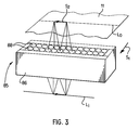
- the most commonly used lenses for this purpose are gradient index fiber lens arrays, as illustrated in Figure 3.
- gradient index lens arrays While commercially available gradient index lens arrays provide good optical efficiency and excellent control of the unity magnification requirement, they have poor depth-of-field capabilities when compared with, for example, reduction optics designs; i. e., they are considerably more sensitive to errors in the object conjugate length than reduction optics designs.
- the depth-of-field for high efficiency gradient index lens arrays is approximately ⁇ 0.25 to ⁇ 0.50 millimeters.
- Figure 4 illustrates the depth-of-field characteristics of a typical gradient index lens array.
- the graph of Figure 4 plots the modulation transfer function (MTF) achievable by the lens array as a function of defocus distance at a predetermined spatial frequency; for example, Figure 4 shows these characteristics for a commercially available lens at 6 cycles per mm.
- the MTF value correlates directly to the fidelity level of the image from the lens array.
- the curves show the defocus distances (or depth-of-field) of the lens array necessary to maintain the desired MTF.
- the zero on the abscissa represents the best focus position and the small divisions along the abscissa are tenths of a millimeter.
- Curve M represents the characteristics of the lens in the main scanning direction along a line coincident with the line of photosensors
- curve S represents the characteristics of the lens in the subscanning direction; i. e., perpendicular to the main scanning direction.
- An object of the invention is to provide a system for improving image fidelity in optical/electrical imaging systems.
- an image input terminal designated generally by the numeral 10, having a platen 12.
- the exemplary image input terminal 10 is a multi-mode, in this case, dual mode, input terminal which in a first mode scans a document original 11 resting face down on platen 12 line by line at a first scan station 13, and in a second mode scans a moving document at a second scan station 14.
- image input terminal 10 converts the document image being scanned to video image signals or pixels which are output to a suitable user (not shown) such as a memory, communication channel, raster output scanner, etc.
- Image input terminal 10 has a suitable frame or housing 18 with base member 20, side members (not shown), end members 24, 25 and top member 26 which cooperate with platen 12 to provide an interior 27 within which a scan carriage 32 is movably disposed.
- Platen 12 which is made of a suitably transparent material, normally glass, is typically rectangular in shape with a length and width sized to accommodate the largest sized document to be scanned by input terminal 10 in the first mode plus the platen area necessary for the second mode.
- scan carriage 32 is supported for back and forth or reciprocating scanning movement (in the direction shown by the solid line arrow of Fig. 1) within the interior 27 of image input terminal 10 by a pair of parallel carriage support rods 34.
- Support rods 34 are suitably mounted on frame 18 in predetermined spaced relation below platen 12 with carriage 32 supported for slidable movement on rods 34 by suitable bearings (not shown).
- a drive screw 37 is threadedly engaged with carriage 32.
- a reversible drive motor 39 rotates screw 37 in either a clockwise or counter-clockwise direction to move the carriage 32 back and forth along carriage support rods 34.
- a linear scanning or image reading photosensor array 40 which may, for example, comprise a Toshiba Model TCD141C CCD chip, is mounted on carriage 32.
- Array 40 has a series (i.e. 5000) of individual photosensitive elements adapted to generate signals having a potential proportional to the reflectance of the object line viewed by the array 40.
- the signals output by array 40 are thereafter input to suitable signal processing circuitry (described below) to provide video image signals or pixels representative of the image scanned.
- An optical system consisting of imaging lens 55 and folding mirrors 56, 57, 58 cooperate to form an optical imaging path 54 through which array 40 views platen 12 and a line-like portion of the document being scanned, the light rays reflected from the document line passing downwardly through platen 12 to mirror 56 and from mirror 56 through mirrors 57, 58 to lens 55 and array 40.
- an illumination assembly 64 consisting of an elongated exposure lamp 65 and cooperating reflector 70 is provided on carriage 32 adjacent the underside of platen 12. Lamp 65 and reflector 70 extend in a direction generally perpendicular to the direction of scanning movement of scan carriage 32. As will be understood, reflector 70 serves to enhance and concentrate light emitted by lamp 65 onto platen 12 at the document line being scanned by array 40.
- scan carriage 32 In the first scan mode, scan carriage 32 is moved by motor 34 from a Start of Scan (SOS) position 72 at one end of platen 12 to an End of Scan (EOS) position 73 and back to SOS position 72.
- SOS Start of Scan
- EOS End of Scan
- Array 40, imaging lens 55, folding mirrors 56, 57, 58 and illumination sensor 64 are fixedly attached to scan carriage 32 and move in unison with the carriage 32.
- EOS position 73 which cooperates with SOS position 72 to delineate first scan station 13, is slightly upstream of the platen end to leave room for a second scan station 14.
- the distance between SOS and EOS positions 72, 73, respectively is chosen to accommodate the largest size document image to be scanned at first scan station 13.
- scan carriage 32 is moved beyond EOS station 73 to a predetermined fixed scan position 74. During scanning in this mode, scan carriage 32 is stationary while the document being scanned is moved past the fixed scan position 74.
- CVT 80 has a plurality of spaced document transport rolls 81 disposed opposite scan position 74, rolls 81 cooperating with the surface 15 of platen 12 opposite thereto to form a document feeding nip 83 therebetween.
- an image input terminal designated generally by the number 90, that employs a full width scanning arrangement. Elements of image input terminal 90 having a structure and function similar to like elements of the image input terminal shown in Figure 1 are similarly numbered.
- the image input terminal 90 is also a multi-mode input terminal, which in a first mode scans a document original 11 resting face down on platen 12 line by line at a first scan station 13, and in a second mode scans a moving document at a second scan station 14.
- imaging input terminal 90 converts the document image being scanned to video image signals or pixels which are output to a suitable user (not shown) such as a memory, communications channel, raster output scanner, etc.
- Image input terminal 90 has a suitable frame or housing 18 with base member 20, end members 24, 25 and top member 26, which cooperate with the platen 12 to provide an interior 27 within which a scan carriage 33 is movably disposed.
- a document 11 placed on platen 12 is scanned in the same manner as described with respect to the Figure 1 terminal.
- the controlled scanning movement is imparted to carriage 33 by drive screw 37 which is threadedly engaged with carriage 33.
- a reversible drive motor 39 rotates screw 37 in forward or reverse directions, thereby moving carriage 33 back and forth along carriage support rods 34.
- the carriage 33 has mounted therein a photosensor array 82 that extends across the carriage 33 in a direction normal to the plane of the drawing.
- the width of the photosensor array 82 corresponds to the maximum width of the document to be imaged on platen 12.
- the illumination assembly 64 comprising the exposure lamp 65 and reflector 70 is mounted on carriage 33 by a suitable mounting arrangement (not shown).
- a gradient index lens array 85 is also mounted on carriage 33.
- the optical axis of the lens array 85 coincides with the optical axis between platen 12 and photosensor array 82, which in the Figure 2 embodiment is substantially vertical.
- the gradient index lens array 85 extends transversely across the carriage 33 in a direction normal to the plane of the drawing.
- the width of the lens array 85 corresponds to the maximum width of the document to be scanned on platen 12 and thus generally corresponds to the width of photosensor array 82.
- an image input terminal can include a two dimensional area array of individual photosensors.
- the photosensitive elements can extend along one direction of the imaged portion of the platen 12, for example the width as in the Figure 1 and Figure 2 scanners, and also along all or a portion of the length of the imaged portion of the platen 12. In this manner, all or a significant portion of the area of a document can be electronically scanned.
- FIG. 3 a typical scanning arrangement using the gradient index lens array 85 is schematically illustrated.
- Successive lines L0 on the document 11 are scanned as the lens array 85 is moved in the direction of arrow S1, which comprises the subscanning direction.
- Line L0 is scanned in a transverse direction of arrow S2 (main scanning direction) electronically by successive scanning of the photosensor array 82, which may, for example, comprise multiple CCD chips, each of which comprises a series of individual photosensitive elements adapted to generate signals having a potential proportional to the reflectance of the object line viewed by the array 82.
- the signals output by array 82 are thereafter input to suitable signal processing circuitry (described below) to provide video image signals or pixels representative of the image scanned.
- the gradient index lens array 85 can comprise, for example, two aligned series of gradient index glass fiber lenses 88.
- An example of such a lens array 85 is the type SLA09 lens sold under the tradename SELFOC by Nippon Sheet Glass.
- Successive lines L0 are imaged through the lens array 85 to form image line L i on photosensor array 82.
- optical image information from a given point (pixel location) on line L0 may pass through one or more of the individual fiber lenses 88, to be imaged on the photosensor array 82.
- Raster scanning of document 11 on platen 12 occurs as a result of the electronic scanning of the linear photosensor array 82, combined with the mechanical motion of the lens 85 and sensor 82 in the subscanning direction.
- the output of the linear photosensor array 82 is an electronic image signal representative of the reflectance information along the single line on the document which lens 85 has imaged onto the sensor array 82. This signal thus represents the information in a row of picture elements, or pixels, which is sampled in the electronic or main scanning direction.
- the sampling pitch in this direction on the document 11 is frequently 12 to 24 samples per mm, as determined by the lens 85 magnification and the spacing of the individual sensors in the linear photosensor array 82.
- Mechanical motion of the sensor 82 and lens 85 in the subscanning direction permits a sequence of rows of pixels to be sensed, with the subscanning pitch or spacing determined by the distance the optical assembly has advanced from the beginning of one electronic line scan to the beginning of the next electronic line scan.
- This subscanning pitch, or separation between rows of pixels is also typically in the range of 12 to 24 rows per mm, although it is not necessarily identical to the pixel pitch within one row.
- Sensor control clocks 91 provide the necessary timing information to the photosensor array 82 to determine the rate at which pixels in a single row are clocked out into the analog signal buffer 92 and the time at which each line scan in the sequence of electronic line scans is to be initiated.
- the analog signal buffer 92 receives this sequence of pixels, one line at a time, and provides the necessary analog signal conditioning (such as signal gain and offset) to properly drive the analog-to-digital (A/D) converter stage 93.
- A/D converter 93 each analog pixel signal is converted into a digital value so that it may be subsequently stored and further processed by digital electronic methods.
- analog pixel signals may be conditioned to vary from 0 volts (representing a point where the document reflectance was 0%) to a value of 1 volt (representing a point where a document reflectance of 95% was sensed).
- the signal, so represented, may be manipulated by conventional digital electronics.
- a linear photosensor array 82 frequently contains between 2000 and 8000 individual photosensor sites which sample the line of information on the document 11 in the electronic scan direction, as previously described. Because of small variations in size and other related parameters, each of these photosensor sites will vary slightly in its photoresponse and dark offset voltage. In high quality reprographic systems it is necessary to compensate for these variations to prevent image defects, such as streaks in the captured image.
- One technique for obtaining such a calibration utilizes a calibration strip 101 which is located on the platen 12 and outside the area to be occupied by the document 11 placed on the platen 12. A common position for calibration strip 101 is between the top of the platen surface 15 and the bottom surface of the document registration guide 100.
- the calibration strip 101 may consist of a uniform high-reflectance area approximately 6 to 10 mm wide and extending the full distance sensed by one line of the photosensor array 82, and an adjacent low-reflectance area of the same size, both areas facing into the scanner towards the lens 85. Under control of the system CPU 99, the lens 85 and photosensor array 82 are positioned so that the linear photosensor array 82 views only the uniform, high-reflectance area of this strip 101.
- the multiplicative factors required to adjust each pixel to a constant output voltage are computed and stored in the pixel calibration RAM 96, one factor for each sensor site in the photosensor array 82.
- the lens 85 and photosensor array 82 are next moved to a position which permits the photosensor array 82 to view the adjacent low-reflectance or black area of the calibration strip 101.
- an additive factor is computed for each pixel which will cause all pixels to produce the same output signal in the presence of little or no light.
- the additive correction factor for each of the individual sensor sites in the photosensor array 82 is also stored in the pixel correction RAM 96.
- the multiplicative and additive correction factors for the individual sensor element which sensed that pixel are read from the pixel calibration RAM 96 and applied to the current pixel signal. In this manner each pixel is corrected for the small deviations in gain and offset which result from the variation in characteristics of the individual sensor elements in the photosensor array 85.
- This calibration technique also compensates for variations in illumination along the photosensor array 82 caused by the lens 85 and lamp 65 characteristics.
- the pixel context 102 for image processing may be expressed in terms of the number of adjacent rows and the number of adjacent pixels in each row required to process the current pixel.
- a 3 X 5 pixel context 102 implies that three adjacent scan lines (or pixel rows) with five pixels from each row are to be used for image processing.
- the position of the pixels may be labeled as shown in Figure 6.
- the pixels are numbered with two indices. The first index represents the scan line position relative to the scan line of the current pixel.
- the second index represents the pixel position along the same scan line relative to the current pixel. If the pixel currently being processed is designated as p 0,0 , then the pixel in the scan line directly above p 0,0 is p -1,0 ; directly to the right is p 0,1 , etc. When a new pixel is to be processed, the new pixel becomes p 0, 0 and the 3 X 5 pixel context 102 shifts to the same relative position about the new pixel. In this example, it is clearly necessary to have pixel signal information available for 3 adjacent scan lines, and this information is stored in the pixel line buffer 95.
- each pixel in the selected pixel context 102 is multiplied by a preselected coefficient stored in the filter coefficient read only memory (ROM) 98 and the resulting products are summed to produce a new value for the current pixel.
- ROM read only memory
- This process is repeated for every pixel, with the selected set of coefficients applied to the new pixel and the surrounding pixels in the new pixel's context. For example, in the 3 X 5 context 102 previously cited, a set of 15 coefficients would be stored in the filter coefficient ROM 98.
- the digital image processing circuit will convert the current pixel, p 0,0 , to a new value, p new , according to
- the filter coefficient ROM 98 may be maintained in the filter coefficient ROM 98, with each set preselected to process a specific type of image. One set may be preferable for continuous tone images, and another set for text images. The appropriate set of coefficients may be manually selected by the operator of the scanner, or may be automatically selected by a circuit (not shown) which recognizes a particular class of images. The coefficient set which is applied to the current pixel may be changed very rapidly; i.e., it may be changed on a pixel-to-pixel basis, if there is a need to do so. It is understood that the System CPU 99 generally coordinates the circuits and activities described above, operating from computer code stored in its associated read only memory (not shown).
- the defocus characteristics of lens 85 are measured and/or computed at several steps or levels of defocus throughout an expected range of focal errors for the purpose of determining appropriate image restoration filters for each step.
- a point spread or line spread function of the selected lens design is determined as a function of defocus error, typically at several steps over a range of 0-4 millimeters of defocus.
- the number of steps or levels within the expected range of defocus at which the point spread function is determined is dependent upon the type of lens 85, the anticipated assembly error for the scanner optical system, and the possible document position errors. Typically, the number of levels at which the point or line spread function would be determined is greater than 2 and less than 10.
- FIG. 7 a typical point spread function is illustrated which was measured in green light for a Nippon Sheet Glass SLA09 lens array when a defocus error of 0.5 mm was introduced.
- This figure illustrates that a point of light on the document 11 is not imaged on the photosensor array 82 as a corresponding point, but has a defocused intensity distribution which blurs over an x-position range of approximately 0.15 mm and over a y-position of approximately 0.10 mm at the photosensor array 82.
- Point spread functions of the type shown in Figure 7 are thus computed or measured and recorded at several defocus positions throughout the range of anticipated defocus errors. For example, they may be recorded for steps of 0.5, 1.0, 1.5, 2.0, 2.5, 3.0, 3.5 and 4.0 mm of defocus, producing a set of eight descriptions of the defocus blur. If the scanner operates in a color separation mode, it may also be necessary to capture this set of eight point spread functions in each of the illuminant colors, if the lens behavior changes significantly with the spectral properties of the illuminant. In this manner, the chromatic aberrations of lens 85 may be taken into account in determining the defocus characteristics of the optical system.
- H(f x , f y ) may take on very small values, approaching zero, the computed inverse restoration filter frequency response, H I (f x , f y ) may take on very high values (relative to unity) at the higher spatial frequencies. This leads to the significant enhancement of any noise in the originally captured image during the remainder of the restoration process which will be subsequently described.
- H(f x , f y ) is the Wiener type filter expressed by where H W (f x , f y ) describes the frequency response of the filter in the two-dimensional spatial frequency domain, S n (f x , f y ) is the noise power spectrum and S f (f x , f y ) is the signal power spectrum.
- a common variant on the Wiener formulation is to replace the ratio of power spectra in the denominator of the above equation with a single constant approximating the system's noise power-to-signal power ratio.
- the inverse and Wiener filter formulations are two of a variety of restoration filter formulations employed in digital filter designs.
- An aspect of this invention is that one of these generally known techniques is employed to compute the appropriate restoration filter frequency response for each of the recorded defocus blur responses; i.e., there is a specific restoration filter design for each step at which the blur response has been recorded. While the symbol H(f x , f y ) was used above to describe the 2-D MTF due to the blurring properties of lens 85 at each level of defocus, it should be clear that other predictable blurring errors, such as the blurring due to the finite size of the sampling aperture on each photosite of the photosensor array 82 may, optionally, be included in H(f x , f y ).
- the pixel coefficients, described previously as a i,j which are to be applied to the current pixel context are obtained from the computed restoration filter frequency response, typically by performing an inverse Fourier transform on the frequency response H W (f x , f y ) or H I (f x , f y ) of the restoration filter. While this theoretically leads to an infinite set of pixel coefficients, all but a few of the coefficients surrounding a 0,0 may be discarded while still maintaining a good approximation to the restoration properties of the computed restoration filter.
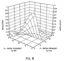
- Figure 9 illustrates a restoration filter frequency response, H I (f x ,f y ), which was computed using the inverse filter formulation, above, for the restoration of an image blurred according to the 0.5 mm defocus error illustrated by the H(f x ,f y ) of Figure 8.
- each of the recorded defocus levels for lens 85 has derived
- a target is placed on the platen glass 12 or on some other convenient structure for establishing the level of defocus correction required to compensate for assembly and component errors existing in a specific assembly.
- the target may comprise an isolated line or a small multiple bar target of known modulation, having a spatial frequency sufficiently high so that it is sensitive to defocus errors.
- the target should be located in a plane which is representative of the position (i.e., object conjugate), of the document or image to be scanned.
- the target may be located in a region of the platen frequently used for calibration targets 101 or under a side registration strip, where it can be monitored periodically during the scanning process.
- the optical system including the lens 85, the photosensor array 82 and the illuminator 64 are caused to be positioned under the known location of the focus measurement target under control of the system CPU 99.
- the image of the target is then projected onto the photosensor array 82, this image containing an amount of optical blur similar to that which will be experienced when document 11 is imaged.
- the digital signal from the photosensor array 82 may then be used, under control of system CPU 99, to compute the reduced modulation of the target, for example, by storing the maximum and minimum signal values obtained while scanning across the multiple bar target and computing modulation as the ratio of the difference of these maximum and minimum values to the sum of these maximum and minimum values. Since the blur characteristics of lens 85 have been previously determined and the focus target has a known spatial frequency and modulation, the reduction in modulation of this target can be correlated directly with one of the previously measured states of defocus. For this purpose a look-up table which identifies one of the previously measured states of defocus with the currently determined reduction in modulation of the focus measurement target is placed in a ROM (not shown) of the system CPU 99.
- the specific state of defocus of the optical system comprising the platen glass 12, the lens 85 and the photosensor array 82 is determined, and this state may be directly identified with one of the previously evaluated levels of defocus and the associated digital filter coefficient set required to correct this defocus level.
- the frequency at which a defocus determination is made is variable.
- the target may be sensed once after final assembly and alignment, using a removable target on the platen, and the required level of defocus correction may be stored for the life of the machine.
- a target may be built into the machine and may be sensed during each machine warmup so that any changes in the optical components (for example, resulting from field replacements) can be compensated.
- the target may be sensed several times during the scan of a single image to correct for object conjugate variations during the scanning process.
- the target may be sensed in each color to detect and correct for defocus resulting from chromatic differences in focus. In this manner, the restoration filter coefficient set used in the digital image processing circuit 97 can be modified for each color, thereby compensating for the chromatic aberrations of the lens 85.
- the restoration of the blurred image is undertaken in the digital image processing circuit 97 using filter coefficients stored in the filter coefficient ROM 98.
- Each of the image restoration coefficient sets determined for the multiple levels of possible optical defocus are stored in the filter coefficient ROM 98. This is preferably accomplished prior to the assembly of the image input terminal, but could be achieved subsequently by replacing the ROM chips with random access memory into which coefficients may be dynamically downloaded at any time.
- the system CPU 99 provides information to the digital image processing circuit 97 indicating which of the predetermined levels of defocus most accurately represents the current machine defocus state. The digital image processing circuit is thus enabled to read and apply to the pixel signal the set of image restoration filter coefficients most appropriate to the machine's current state of defocus.
- the automatic detection of focus state and subsequent selection of optimum restoration filter coefficients is the preferred operating mode, it may be desirable under certain circumstances to manually override this selection. For example, if a relatively noisy document is to be imaged, the automatically selected restoration filter may provide excessive enhancement of high frequency noise. In such cases it is desirable to permit the user to enter information on a user interface (not shown) which signals the system CPU 99 to substitute a user designated filter selection in place of the automatically sensed selection.
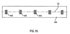
- Such multiple states of defocus along one scan line may be detected and corrected using a multiplicity of focus detection targets in a location which may be sensed by the scan line.
- a strip of material 104 which may be, for example, mounted on the platen 12 with focus measurement targets 105 facing the full-width lens 85 or single lens 55. Mechanically placing the optical system such that a line in the main scanning direction senses targets 105 as indicated along line L o , will permit the state of focus to be detected at multiple positions along a single scan line.
- Such multiple states are computed and communicated to the digital image processing circuit 97 prior to the start of the scanning of document 11.
- the restoration filter coefficients appropriate to the current pixel's position along the scan line are correctly identified and applied.
- This approach to correction of multiple states of defocus within a document may similarly be extended to focus variations in the subscanning direction by mounting and sensing a multiple target strip of the type shown in Figure 10 along the edge of a document which is perpendicular to the main scanning direction.
- the depth of field of a scanner system can be electronically enhanced in an adaptive manner to maximize image reproduction fidelity.
- the system compensates for focus errors induced by optical component and alignment tolerances.
- the system permits relaxation of these tolerances while maintaining image quality.
Landscapes
- Engineering & Computer Science (AREA)
- Multimedia (AREA)
- Signal Processing (AREA)
- Health & Medical Sciences (AREA)
- Biomedical Technology (AREA)
- General Health & Medical Sciences (AREA)
- Facsimile Scanning Arrangements (AREA)
- Facsimile Image Signal Circuits (AREA)
Abstract
Description
- This invention relates to optical imaging systems in electronic reprographic equipment. More specifically, the invention relates to a system for correction of optical defocus and related optical system errors by correction of electrical signals representative of the optically produced image data.
- Electronic reprographic equipment and facsimile transmission equipment employ scanners for optically scanning an image, such as a document, and converting the optical information to an electrical image signal. Several types of optical systems are commonly employed to achieve the raster scanning of input documents and produce the representative electrical signal. Figure 1 illustrates one of several configurations frequently used with reduction optical systems to scan a document and produce a reduced size image on a linear array of photosensors. This configuration is relatively tolerant of errors in the object conjugate of the lens; i.e., errors in the optical path length from the lens, through the mirrors, to the original document. Variations in this path length of ± 1 millimeters, while causing noticeable change in magnification, will typically have little degrading effect on the focus, or sharpness, of the optical image formed on the photosensor array. Since only one compound lens is used, however, there may exist a variation in image quality along the linear portion of the image sensed by the photosensor array. Variations in image quality from the end of such a scanned image line to the center of this line frequently occur with a reasonable degree of symmetry about the center of the scanned image. These variations in quality may, for example, be caused by the curvature of the surface of best focus of the lens, or by other related lens aberrations which are well known to vary with the distance from the center of the optical field. The mathematical description of these aberrations can be approximately determined from lens design data, but further aberrations occur due to small errors which result from the lens fabrication process. Other single lens optical systems, such as those frequently referred to as "full-rate / half-rate" scanners, have similar optical characteristics. As a result, scanners using single reduction lens optics may illustrate a decrease in image quality at the edges of the scan line, even when the center of scan is in good focus.
- A second class of optical systems frequently used for document scanning in electronic reprographic equipment is the "full-width" scanner type, shown in Figure 2. Here, an array of lenses extends (into the page in the figure) the full extent of the line on the input document which is to be imaged at unity magnification onto the full-width photosensor array. Full-width scanners have been developed which utilize amorphous or crystalline silicon photosensor arrays that offer the advantages of high responsivity (which yields high scanning speeds), low illumination requirements (which reduces power consumption) and compactness. These scanners require compact, full width lens arrays to achieve these performance advantages. The most commonly used lenses for this purpose are gradient index fiber lens arrays, as illustrated in Figure 3. While commercially available gradient index lens arrays provide good optical efficiency and excellent control of the unity magnification requirement, they have poor depth-of-field capabilities when compared with, for example, reduction optics designs; i. e., they are considerably more sensitive to errors in the object conjugate length than reduction optics designs. Typically, the depth-of-field for high efficiency gradient index lens arrays is approximately ± 0.25 to ± 0.50 millimeters.
- Figure 4 illustrates the depth-of-field characteristics of a typical gradient index lens array. The graph of Figure 4 plots the modulation transfer function (MTF) achievable by the lens array as a function of defocus distance at a predetermined spatial frequency; for example, Figure 4 shows these characteristics for a commercially available lens at 6 cycles per mm. The MTF value correlates directly to the fidelity level of the image from the lens array. By selecting a desired level of MTF (and thus image fidelity) the curves show the defocus distances (or depth-of-field) of the lens array necessary to maintain the desired MTF. In Figure 4, the zero on the abscissa represents the best focus position and the small divisions along the abscissa are tenths of a millimeter. Curve M represents the characteristics of the lens in the main scanning direction along a line coincident with the line of photosensors, and curve S represents the characteristics of the lens in the subscanning direction; i. e., perpendicular to the main scanning direction. From Figure 4, it is evident that at high levels of image fidelity (MTF), small variations in defocus distance can cause unacceptable blurring and that the amount of blur varies with the scan direction (i.e., the lens becomes increasingly anamorphic in this loss of quality as the focus error increases). As a result, optics/sensor architectures employing such full-width lens arrays frequently do not provide sufficient image quality or resolution to meet image fidelity requirements, thereby limiting the use of such scanner designs.
- An object of the invention is to provide a system for improving image fidelity in optical/electrical imaging systems.
- It is an object of this invention to provide image defocus correction in systems using optics having a limited depth-of-field.
- It is a further object of this invention to provide correction of other predictable optical errors which may occur in varying amounts throughout the field of the imaging system.
- These objects are achieved in a system wherein the characteristics of the optical image data representative of a plurality of states of defocus or optical field position of the system are predetermined, and filter coefficients for the correction of these states are stored in the scanner system. The defocused or degraded state of a specific scanner system is then determined by use of one or more standard reference targets. Electrical image data from the photosensor array is then filtered with a fixed or time-varying image restoration filter which utilizes correction coefficients preselected to be appropriate for the state of system defocus or degradation previously determined.
- An optical image system in accordance with the invention will now be described, by way of example, with reference to the accompanying drawings, in which:-
- Figure 1 is a schematic illustration of a reduction optical system employed in a document scanning system;
- Figure 2 is a schematic illustration of a unity magnification, full-width optical system employed in a document scanning system;
- Figure 3 is an illustration of a typical two-row gradient lens array designed for unity magnification;
- Figure 4 is a graph showing modulation transfer functions of a typical index gradient lens array relative to defocus distance;
- Figure 5 is a schematic illustration of an image scanning system illustrating the circuit functions which may be employed to enable an embodiment of this invention;
- Figure 6 is an illustration of a portion of the document to be scanned, demonstrating the pixel context used by the digital image processing filter;
- Figure 7 is an illustration of the optical point spread function of a commercial gradient index lens array when a defocus error of 0.5 mm is introduced;
- Figure 8 is an illustration of the two-dimensional modulation transfer function derived from the point spread function illustrated in Figure 7;
- Figure 9 is an illustration of the frequency response of an image restoration filter designed to remove the defocus blur of a commercial gradient index lens array having the characteristics shown in Figures 7 and 8;
- Figure 10 is an illustration of a focus measurement strip containing multiple focus measurement targets.
- Referring to Figure 1 of the drawings, there is shown an image input terminal, designated generally by the
numeral 10, having aplaten 12. The exemplaryimage input terminal 10 is a multi-mode, in this case, dual mode, input terminal which in a first mode scans a document original 11 resting face down onplaten 12 line by line at afirst scan station 13, and in a second mode scans a moving document at asecond scan station 14. As will appear more fully herein,image input terminal 10 converts the document image being scanned to video image signals or pixels which are output to a suitable user (not shown) such as a memory, communication channel, raster output scanner, etc. -
Image input terminal 10 has a suitable frame orhousing 18 withbase member 20, side members (not shown),end members top member 26 which cooperate withplaten 12 to provide aninterior 27 within which ascan carriage 32 is movably disposed.Platen 12, which is made of a suitably transparent material, normally glass, is typically rectangular in shape with a length and width sized to accommodate the largest sized document to be scanned byinput terminal 10 in the first mode plus the platen area necessary for the second mode. - For the first mode,
scan carriage 32 is supported for back and forth or reciprocating scanning movement (in the direction shown by the solid line arrow of Fig. 1) within theinterior 27 ofimage input terminal 10 by a pair of parallelcarriage support rods 34.Support rods 34 are suitably mounted onframe 18 in predetermined spaced relation belowplaten 12 withcarriage 32 supported for slidable movement onrods 34 by suitable bearings (not shown). - To impart controlled scanning movement to
carriage 32, adrive screw 37 is threadedly engaged withcarriage 32. Areversible drive motor 39 rotatesscrew 37 in either a clockwise or counter-clockwise direction to move thecarriage 32 back and forth alongcarriage support rods 34. - A linear scanning or image
reading photosensor array 40, which may, for example, comprise a Toshiba Model TCD141C CCD chip, is mounted oncarriage 32.Array 40 has a series (i.e. 5000) of individual photosensitive elements adapted to generate signals having a potential proportional to the reflectance of the object line viewed by thearray 40. The signals output byarray 40 are thereafter input to suitable signal processing circuitry (described below) to provide video image signals or pixels representative of the image scanned. - An optical system consisting of
imaging lens 55 andfolding mirrors optical imaging path 54 through whicharray 40views platen 12 and a line-like portion of the document being scanned, the light rays reflected from the document line passing downwardly throughplaten 12 tomirror 56 and frommirror 56 throughmirrors lens 55 andarray 40. To illuminate the document line being scanned, anillumination assembly 64 consisting of anelongated exposure lamp 65 and cooperatingreflector 70 is provided oncarriage 32 adjacent the underside ofplaten 12.Lamp 65 andreflector 70 extend in a direction generally perpendicular to the direction of scanning movement ofscan carriage 32. As will be understood,reflector 70 serves to enhance and concentrate light emitted bylamp 65 ontoplaten 12 at the document line being scanned byarray 40. - In the first scan mode,
scan carriage 32 is moved bymotor 34 from a Start of Scan (SOS)position 72 at one end ofplaten 12 to an End of Scan (EOS)position 73 and back toSOS position 72.Array 40,imaging lens 55,folding mirrors illumination sensor 64 are fixedly attached to scancarriage 32 and move in unison with thecarriage 32. EOSposition 73, which cooperates withSOS position 72 to delineatefirst scan station 13, is slightly upstream of the platen end to leave room for asecond scan station 14. As will be understood, the distance between SOS andEOS positions first scan station 13. - In the second scan mode, scan
carriage 32 is moved beyondEOS station 73 to a predetermined fixedscan position 74. During scanning in this mode, scancarriage 32 is stationary while the document being scanned is moved past the fixedscan position 74. - To move the
document 11 to be scanned past the fixedscan position 74, a Constant Velocity Transport (CVT) 80 is provided.CVT 80 has a plurality of spaced document transport rolls 81 disposedopposite scan position 74, rolls 81 cooperating with thesurface 15 ofplaten 12 opposite thereto to form a document feeding nip 83 therebetween. - Referring to Figure 2 of the drawings, there is shown an image input terminal, designated generally by the
number 90, that employs a full width scanning arrangement. Elements ofimage input terminal 90 having a structure and function similar to like elements of the image input terminal shown in Figure 1 are similarly numbered. Theimage input terminal 90 is also a multi-mode input terminal, which in a first mode scans a document original 11 resting face down onplaten 12 line by line at afirst scan station 13, and in a second mode scans a moving document at asecond scan station 14. In the same fashion asimaging input terminal 10,imaging input terminal 90 converts the document image being scanned to video image signals or pixels which are output to a suitable user (not shown) such as a memory, communications channel, raster output scanner, etc. -
Image input terminal 90 has a suitable frame orhousing 18 withbase member 20,end members top member 26, which cooperate with theplaten 12 to provide an interior 27 within which ascan carriage 33 is movably disposed. Adocument 11 placed onplaten 12 is scanned in the same manner as described with respect to the Figure 1 terminal. In the first or reciprocating scan mode, the controlled scanning movement is imparted tocarriage 33 bydrive screw 37 which is threadedly engaged withcarriage 33. Areversible drive motor 39 rotates screw 37 in forward or reverse directions, thereby movingcarriage 33 back and forth alongcarriage support rods 34. - In this scanner, the
carriage 33 has mounted therein aphotosensor array 82 that extends across thecarriage 33 in a direction normal to the plane of the drawing. The width of thephotosensor array 82 corresponds to the maximum width of the document to be imaged onplaten 12. Theillumination assembly 64 comprising theexposure lamp 65 andreflector 70 is mounted oncarriage 33 by a suitable mounting arrangement (not shown). A gradientindex lens array 85 is also mounted oncarriage 33. The optical axis of thelens array 85 coincides with the optical axis betweenplaten 12 andphotosensor array 82, which in the Figure 2 embodiment is substantially vertical. The gradientindex lens array 85 extends transversely across thecarriage 33 in a direction normal to the plane of the drawing. The width of thelens array 85 corresponds to the maximum width of the document to be scanned onplaten 12 and thus generally corresponds to the width ofphotosensor array 82. - Alternatively, an image input terminal can include a two dimensional area array of individual photosensors. In such an array, the photosensitive elements can extend along one direction of the imaged portion of the
platen 12, for example the width as in the Figure 1 and Figure 2 scanners, and also along all or a portion of the length of the imaged portion of theplaten 12. In this manner, all or a significant portion of the area of a document can be electronically scanned. - Referring to Figure 3, a typical scanning arrangement using the gradient
index lens array 85 is schematically illustrated. Successive lines L₀ on thedocument 11 are scanned as thelens array 85 is moved in the direction of arrow S1, which comprises the subscanning direction. Line L₀ is scanned in a transverse direction of arrow S2 (main scanning direction) electronically by successive scanning of thephotosensor array 82, which may, for example, comprise multiple CCD chips, each of which comprises a series of individual photosensitive elements adapted to generate signals having a potential proportional to the reflectance of the object line viewed by thearray 82. As described previously, the signals output byarray 82 are thereafter input to suitable signal processing circuitry (described below) to provide video image signals or pixels representative of the image scanned. - The gradient
index lens array 85 can comprise, for example, two aligned series of gradient indexglass fiber lenses 88. An example of such alens array 85 is the type SLA09 lens sold under the tradename SELFOC by Nippon Sheet Glass. Successive lines L₀ are imaged through thelens array 85 to form image line Li onphotosensor array 82. As shown in Figure 3, optical image information from a given point (pixel location) on line L₀ may pass through one or more of theindividual fiber lenses 88, to be imaged on thephotosensor array 82. - Referring to Figure 5, the basic functions of a typical electronic reprographic scanner capable of embodying the invention are illustrated. Raster scanning of
document 11 onplaten 12 occurs as a result of the electronic scanning of thelinear photosensor array 82, combined with the mechanical motion of thelens 85 andsensor 82 in the subscanning direction. At each position in the subscanning direction, the output of thelinear photosensor array 82 is an electronic image signal representative of the reflectance information along the single line on the document whichlens 85 has imaged onto thesensor array 82. This signal thus represents the information in a row of picture elements, or pixels, which is sampled in the electronic or main scanning direction. The sampling pitch in this direction on thedocument 11 is frequently 12 to 24 samples per mm, as determined by thelens 85 magnification and the spacing of the individual sensors in thelinear photosensor array 82. Mechanical motion of thesensor 82 andlens 85 in the subscanning direction permits a sequence of rows of pixels to be sensed, with the subscanning pitch or spacing determined by the distance the optical assembly has advanced from the beginning of one electronic line scan to the beginning of the next electronic line scan. This subscanning pitch, or separation between rows of pixels, is also typically in the range of 12 to 24 rows per mm, although it is not necessarily identical to the pixel pitch within one row. - Sensor control clocks 91 provide the necessary timing information to the
photosensor array 82 to determine the rate at which pixels in a single row are clocked out into theanalog signal buffer 92 and the time at which each line scan in the sequence of electronic line scans is to be initiated. Theanalog signal buffer 92 receives this sequence of pixels, one line at a time, and provides the necessary analog signal conditioning (such as signal gain and offset) to properly drive the analog-to-digital (A/D)converter stage 93. In the A/D converter 93, each analog pixel signal is converted into a digital value so that it may be subsequently stored and further processed by digital electronic methods. For example, analog pixel signals may be conditioned to vary from 0 volts (representing a point where the document reflectance was 0%) to a value of 1 volt (representing a point where a document reflectance of 95% was sensed). The A/D converter 93 will then convert this continuous analog voltage range into a discrete set of digital numbers. For example, if an 8-bit A/D converter is used, the signal is converted to one of the 2⁸ = 256 levels which can be represented by an 8-bit binary number. The signal, so represented, may be manipulated by conventional digital electronics. - It is also common practice to include pixel correction capability in the signal processing, as shown in Figure 5. A
linear photosensor array 82 frequently contains between 2000 and 8000 individual photosensor sites which sample the line of information on thedocument 11 in the electronic scan direction, as previously described. Because of small variations in size and other related parameters, each of these photosensor sites will vary slightly in its photoresponse and dark offset voltage. In high quality reprographic systems it is necessary to compensate for these variations to prevent image defects, such as streaks in the captured image. One technique for obtaining such a calibration utilizes acalibration strip 101 which is located on theplaten 12 and outside the area to be occupied by thedocument 11 placed on theplaten 12. A common position forcalibration strip 101 is between the top of theplaten surface 15 and the bottom surface of thedocument registration guide 100. Thecalibration strip 101 may consist of a uniform high-reflectance area approximately 6 to 10 mm wide and extending the full distance sensed by one line of thephotosensor array 82, and an adjacent low-reflectance area of the same size, both areas facing into the scanner towards thelens 85. Under control of thesystem CPU 99, thelens 85 andphotosensor array 82 are positioned so that thelinear photosensor array 82 views only the uniform, high-reflectance area of thisstrip 101. The multiplicative factors required to adjust each pixel to a constant output voltage are computed and stored in thepixel calibration RAM 96, one factor for each sensor site in thephotosensor array 82. Thelens 85 andphotosensor array 82 are next moved to a position which permits thephotosensor array 82 to view the adjacent low-reflectance or black area of thecalibration strip 101. Here an additive factor is computed for each pixel which will cause all pixels to produce the same output signal in the presence of little or no light. The additive correction factor for each of the individual sensor sites in thephotosensor array 82 is also stored in thepixel correction RAM 96. During subsequent document scanning, as the signal from each pixel passes through thepixel correction circuit 94, the multiplicative and additive correction factors for the individual sensor element which sensed that pixel are read from thepixel calibration RAM 96 and applied to the current pixel signal. In this manner each pixel is corrected for the small deviations in gain and offset which result from the variation in characteristics of the individual sensor elements in thephotosensor array 85. This calibration technique also compensates for variations in illumination along thephotosensor array 82 caused by thelens 85 andlamp 65 characteristics. - Several scan lines of the corrected pixels are then stored in the
pixel line buffer 95. This is required because subsequent image processing may utilize the signals from pixels which are adjacent to the currently processed pixel in both the main scanning and subscanning direction. Referring to Figure 6, thepixel context 102 for image processing may be expressed in terms of the number of adjacent rows and the number of adjacent pixels in each row required to process the current pixel. For example, a 3X 5pixel context 102 implies that three adjacent scan lines (or pixel rows) with five pixels from each row are to be used for image processing. The position of the pixels may be labeled as shown in Figure 6. The pixels are numbered with two indices. The first index represents the scan line position relative to the scan line of the current pixel. The second index represents the pixel position along the same scan line relative to the current pixel. If the pixel currently being processed is designated as p0,0, then the pixel in the scan line directly above p0,0 is p-1,0; directly to the right is p0,1, etc. When a new pixel is to be processed, the new pixel becomesp 0,₀ and the 3X 5pixel context 102 shifts to the same relative position about the new pixel. In this example, it is clearly necessary to have pixel signal information available for 3 adjacent scan lines, and this information is stored in thepixel line buffer 95. - These multiple lines of pixel signal information are next made available to the digital
image processing circuit 97. In this circuit, each pixel in the selectedpixel context 102 is multiplied by a preselected coefficient stored in the filter coefficient read only memory (ROM) 98 and the resulting products are summed to produce a new value for the current pixel. This process is repeated for every pixel, with the selected set of coefficients applied to the new pixel and the surrounding pixels in the new pixel's context. For example, in the 3X 5context 102 previously cited, a set of 15 coefficients would be stored in thefilter coefficient ROM 98. If these are labeled asa-1,-2 a-1,-1 a-1,0 a-1,1 a-1,2 a0,-2 a0,-1 a0,0 a0,1 a0,2 a1,-2 a1,-1 a1,0 a1,1 a1,2
to correspond with the associated pixel in the 3X 5context 102, the digital image processing circuit will convert the current pixel, p0,0, to a new value, pnew, according to
- When the next pixel is to be processed, its new context may be similarly processed by this set of coefficients to generate a new value for this next pixel. Multiple coefficient sets may be maintained in the
filter coefficient ROM 98, with each set preselected to process a specific type of image. One set may be preferable for continuous tone images, and another set for text images. The appropriate set of coefficients may be manually selected by the operator of the scanner, or may be automatically selected by a circuit (not shown) which recognizes a particular class of images. The coefficient set which is applied to the current pixel may be changed very rapidly; i.e., it may be changed on a pixel-to-pixel basis, if there is a need to do so. It is understood that theSystem CPU 99 generally coordinates the circuits and activities described above, operating from computer code stored in its associated read only memory (not shown). - In order to improve the quality of the image data supplied by the
photosensor array 82 in the presence of defocus errors introduced bylens 85, a three-step image restoration process is applied. The three steps are: - (1) Determine by measurement and/or computation the defocus imaging characteristics of the
lens 85 at several levels of defocus throughout the expected range of focal errors, and compute appropriate image restoration filters for each level; - (2) Enable the image input terminal to dynamically measure its present state of defocus by scanning appropriately located focus measurement targets, thus establishing the level of defocus correction required to compensate for component and assembly errors; and
- (3) Using digital image processing circuits, select the set of image restoration filter coefficients indicated by the present state of defocus and apply these coefficients to the image signal.
- In a first step, the defocus characteristics of
lens 85 are measured and/or computed at several steps or levels of defocus throughout an expected range of focal errors for the purpose of determining appropriate image restoration filters for each step. In order to do so, a point spread or line spread function of the selected lens design is determined as a function of defocus error, typically at several steps over a range of 0-4 millimeters of defocus. The number of steps or levels within the expected range of defocus at which the point spread function is determined is dependent upon the type oflens 85, the anticipated assembly error for the scanner optical system, and the possible document position errors. Typically, the number of levels at which the point or line spread function would be determined is greater than 2 and less than 10. - Because of the anamorphic nature of the lens array characteristics as previously described with reference to Figure 4, it is preferable to characterize these lenses using the two-dimensional point spread function, thus capturing the image degrading characteristics for all directions on the document. Referring to Figure 7, a typical point spread function is illustrated which was measured in green light for a Nippon Sheet Glass SLA09 lens array when a defocus error of 0.5 mm was introduced. This figure illustrates that a point of light on the
document 11 is not imaged on thephotosensor array 82 as a corresponding point, but has a defocused intensity distribution which blurs over an x-position range of approximately 0.15 mm and over a y-position of approximately 0.10 mm at thephotosensor array 82. The multiple peaks in this point spread function are caused by the failure of the contributions from adjacent lenses in the array to converge to the same point in the defocused image plane. Point spread functions of the type shown in Figure 7 are thus computed or measured and recorded at several defocus positions throughout the range of anticipated defocus errors. For example, they may be recorded for steps of 0.5, 1.0, 1.5, 2.0, 2.5, 3.0, 3.5 and 4.0 mm of defocus, producing a set of eight descriptions of the defocus blur. If the scanner operates in a color separation mode, it may also be necessary to capture this set of eight point spread functions in each of the illuminant colors, if the lens behavior changes significantly with the spectral properties of the illuminant. In this manner, the chromatic aberrations oflens 85 may be taken into account in determining the defocus characteristics of the optical system. - It is common practice, and useful in the design of digital filters, to describe each of the defocus point spread functions in a two-dimensional spatial frequency domain. This is achieved by computing the two-dimensional Fourier transform of the point spread function and normalizing the result at the zero-frequency origin to unity. This is a procedure well known in the fields of optical system analysis and digital filter design, and the resulting function is known as the two-dimensional modulation transfer function, or 2-D MTF. For example, Figure 8 is a plot of the 2-D MTF so computed from the 0.5 mm defocus point spread function of Figure 7. In this manner, each of the recorded point spread functions over the focal range is transformed to produce a corresponding set of 2-D MTF's.
- In order to correct the undesirable blurring of the signal it is necessary to design a digital image restoration filter for each of the recorded blur functions, using the information computed in the set of 2-D MTF's above. One approach to the design of a compensating filter is to use the inverse filter. If the 2-D MTF surface for a particular blurred image condition, such as the shown in Figure 8, is represented by the symbol, H(fx, fy), then an inverse restoration filter may be computed from

where HI(fx, fy) describes the frequency response of the filter in the two-dimensional spatial frequency domain, and fx and fy represent the frequency axis variables in the main and subscanning directions, respectively. Because the original blurred 2-D MTF, H(fx, fy) may take on very small values, approaching zero, the computed inverse restoration filter frequency response, HI(fx, fy) may take on very high values (relative to unity) at the higher spatial frequencies. This leads to the significant enhancement of any noise in the originally captured image during the remainder of the restoration process which will be subsequently described. An alternate formulation for computing a desired restoration filter for the 2-D MTF function, H(fx, fy) is the Wiener type filter expressed by
where HW(fx, fy) describes the frequency response of the filter in the two-dimensional spatial frequency domain, Sn(fx, fy) is the noise power spectrum and Sf(fx, fy) is the signal power spectrum. A common variant on the Wiener formulation is to replace the ratio of power spectra in the denominator of the above equation with a single constant approximating the system's noise power-to-signal power ratio. The inverse and Wiener filter formulations are two of a variety of restoration filter formulations employed in digital filter designs. An aspect of this invention is that one of these generally known techniques is employed to compute the appropriate restoration filter frequency response for each of the recorded defocus blur responses; i.e., there is a specific restoration filter design for each step at which the blur response has been recorded. While the symbol H(fx, fy) was used above to describe the 2-D MTF due to the blurring properties oflens 85 at each level of defocus, it should be clear that other predictable blurring errors, such as the blurring due to the finite size of the sampling aperture on each photosite of thephotosensor array 82 may, optionally, be included in H(fx, fy). - As a final part of the filter design process, the pixel coefficients, described previously as ai,j, which are to be applied to the current pixel context are obtained from the computed restoration filter frequency response, typically by performing an inverse Fourier transform on the frequency response HW(fx, fy) or HI(fx, fy) of the restoration filter. While this theoretically leads to an infinite set of pixel coefficients, all but a few of the coefficients surrounding a0,0 may be discarded while still maintaining a good approximation to the restoration properties of the computed restoration filter. As an example of this final operation, Figure 9 illustrates a restoration filter frequency response, HI(fx,fy), which was computed using the inverse filter formulation, above, for the restoration of an image blurred according to the 0.5 mm defocus error illustrated by the H(fx,fy) of Figure 8. The inverse Fourier transform of the frequency response shown in Figure 9, after dropping the less significant values, yields a set of coefficients, aij, which may be applied to the current pixel, as above described, to restore the blurred image to a quality approaching the original image. The resulting aij for this example use a 5
X 5 pixel context, and are given bya-2,-2 a-2,-1 a-2,0 a-2,1 a-2,2 -0.0014-0.0007 0.0501 -0.0007-0.0014 a-1,-2 a-1,-1 a-1,0 a-1,1 a-1,2 0.0742 -0.2281 0.0141 -0.2331 0.0770 a0,-2 a0,-1 a0,0 a0,1 a0,2 = 0.1222 -1.7161 4.6879 -1.7161 0.1222 a1,-2 a1,-1 a1,0 a1,1 a1,2 0.0770 -0.2331 0.0141 -0.2281 0.0742 a2,-2 a2,-1 a2,0 a2,1 a2,2 -0.0014-0.0007 0.0501 -0.0007-0.0014
In this manner, each of the recorded defocus levels forlens 85 has derived, according to known techniques, a corresponding set of restoration coefficients. The computation of these restoration coefficients completes the first step of the invention. These restoration coefficients are utilized to significantly reduce the detrimental effects of defocus blur and associated imaging errors on the digitally processed image signal. - In a second step, the actual state of focus of the optical system as mounted in a particular piece of equipment is determined. In order to dynamically measure the state of defocus in a specific scanner structure, a target is placed on the
platen glass 12 or on some other convenient structure for establishing the level of defocus correction required to compensate for assembly and component errors existing in a specific assembly. The target may comprise an isolated line or a small multiple bar target of known modulation, having a spatial frequency sufficiently high so that it is sensitive to defocus errors. Ideally, the target should be located in a plane which is representative of the position (i.e., object conjugate), of the document or image to be scanned. For example, the target may be located in a region of the platen frequently used forcalibration targets 101 or under a side registration strip, where it can be monitored periodically during the scanning process. The optical system, including thelens 85, thephotosensor array 82 and theilluminator 64 are caused to be positioned under the known location of the focus measurement target under control of thesystem CPU 99. The image of the target is then projected onto thephotosensor array 82, this image containing an amount of optical blur similar to that which will be experienced whendocument 11 is imaged. The digital signal from thephotosensor array 82 may then be used, under control ofsystem CPU 99, to compute the reduced modulation of the target, for example, by storing the maximum and minimum signal values obtained while scanning across the multiple bar target and computing modulation as the ratio of the difference of these maximum and minimum values to the sum of these maximum and minimum values. Since the blur characteristics oflens 85 have been previously determined and the focus target has a known spatial frequency and modulation, the reduction in modulation of this target can be correlated directly with one of the previously measured states of defocus. For this purpose a look-up table which identifies one of the previously measured states of defocus with the currently determined reduction in modulation of the focus measurement target is placed in a ROM (not shown) of thesystem CPU 99. In this manner, the specific state of defocus of the optical system comprising theplaten glass 12, thelens 85 and thephotosensor array 82 is determined, and this state may be directly identified with one of the previously evaluated levels of defocus and the associated digital filter coefficient set required to correct this defocus level. - The frequency at which a defocus determination is made is variable. For example, the target may be sensed once after final assembly and alignment, using a removable target on the platen, and the required level of defocus correction may be stored for the life of the machine. Alternatively, a target may be built into the machine and may be sensed during each machine warmup so that any changes in the optical components (for example, resulting from field replacements) can be compensated. Alternatively, the target may be sensed several times during the scan of a single image to correct for object conjugate variations during the scanning process. For color document scanners, the target may be sensed in each color to detect and correct for defocus resulting from chromatic differences in focus. In this manner, the restoration filter coefficient set used in the digital
image processing circuit 97 can be modified for each color, thereby compensating for the chromatic aberrations of thelens 85. - In the final step, the restoration of the blurred image is undertaken in the digital
image processing circuit 97 using filter coefficients stored in thefilter coefficient ROM 98. Each of the image restoration coefficient sets determined for the multiple levels of possible optical defocus are stored in thefilter coefficient ROM 98. This is preferably accomplished prior to the assembly of the image input terminal, but could be achieved subsequently by replacing the ROM chips with random access memory into which coefficients may be dynamically downloaded at any time. After the current state of defocus of the image input terminal is determined according to the previously described process, thesystem CPU 99 provides information to the digitalimage processing circuit 97 indicating which of the predetermined levels of defocus most accurately represents the current machine defocus state. The digital image processing circuit is thus enabled to read and apply to the pixel signal the set of image restoration filter coefficients most appropriate to the machine's current state of defocus. - While the automatic detection of focus state and subsequent selection of optimum restoration filter coefficients is the preferred operating mode, it may be desirable under certain circumstances to manually override this selection. For example, if a relatively noisy document is to be imaged, the automatically selected restoration filter may provide excessive enhancement of high frequency noise. In such cases it is desirable to permit the user to enter information on a user interface (not shown) which signals the
system CPU 99 to substitute a user designated filter selection in place of the automatically sensed selection. - In the foregoing description it has been assumed that a single defocus state can be detected and the appropriately selected single set of image restoration filter coefficients will be applied to all pixels in the scanned document's image signal. It is possible, however, that the state of focus may vary from one part of the document to another part. This may occur if the gradient
index lens array 85 is not accurately parallel to the platen glass. It may also occur due to the natural increase in blur that can occur as the ends of a scan line are sensed with asingle lens 55 as previously described in reference to the reduction optical architectures of Figure 1. In these instances there may be several distinct states of defocus along the main scan line. Such multiple states of defocus along one scan line may be detected and corrected using a multiplicity of focus detection targets in a location which may be sensed by the scan line. Referring to Figure 10, there is shown a strip ofmaterial 104 which may be, for example, mounted on theplaten 12 withfocus measurement targets 105 facing the full-width lens 85 orsingle lens 55. Mechanically placing the optical system such that a line in the main scanning direction sensestargets 105 as indicated along line Lo, will permit the state of focus to be detected at multiple positions along a single scan line. Such multiple states are computed and communicated to the digitalimage processing circuit 97 prior to the start of the scanning ofdocument 11. Thus during the scanning ofdocument 11, the restoration filter coefficients appropriate to the current pixel's position along the scan line are correctly identified and applied. This approach to correction of multiple states of defocus within a document may similarly be extended to focus variations in the subscanning direction by mounting and sensing a multiple target strip of the type shown in Figure 10 along the edge of a document which is perpendicular to the main scanning direction. In this latter arrangement it may be desirable to rotate the individualfocus measurement targets 105 by 90°, or provide targets with 0° and 90° rotation to permit defocus measurement in both scanning directions. - From the foregoing, it can be seen that the depth of field of a scanner system can be electronically enhanced in an adaptive manner to maximize image reproduction fidelity. The system compensates for focus errors induced by optical component and alignment tolerances. The system permits relaxation of these tolerances while maintaining image quality.
This process will be described with reference to a full-width scanning system as shown in Figure 2 which is assumed to have the functional capabilities of a scanner detailed in Figure 5. The further applicability of this process to scanners of the single lens type as shown in Figure 1 will be made apparent by subsequent descriptions.
Claims (10)
- Image scanning apparatus comprising:
an image support(12);
a scanner for scanning an image on the image support, said scanner comprising an optical element (55 or 85) for receiving optical image data from an image on the image support and a photoreceptor (40 or 82) for receiving optical image data from the optical element and converting the optical data to an electrical data signal;
providing means for providing a plurality of sets of image restoration data, each set of image restoration data being representative of a different one of a plurality of defocus states of the optical image data received by the photoreceptor from the optical elements;
determining means for determining a defocus state of optical image data on the photoreceptor;
selecting means (98) for selecting one of the sets of image restoration data provided by the providing means based on the defocus state determined by the determining means;
signal processing means (97) for receiving the electrical data signal from the photoreceptor and a set of image restoration data from the selecting means (98) and modifying the electrical data signal in accordance with the image restoration data received from the selecting means. - Apparatus as in claim 1, wherein the providing means comprises a memory for storing the plurality of sets of image restoration data.
- Apparatus as in claim 1, wherein the providing means utilizes a Weiner filter to compute the image restoration data.
- Apparatus as in claim 1, further including means for providing image quality data to the processing means indicative of the quality of an image on the image support.
- Apparatus as in claim 1, further comprising a focus target and wherein the determining means determines one of a plurality of levels of defocus of the optical system formed by the image support and the scanner from image data from the focus target.
- Apparatus as in claim 1, wherein the optical element is a lens, an array of lenses, or a gradient index lens array.
- Apparatus as in claim 1, wherein the photoreceptor comprises a linear or area array of photosensitive elements.
- A method for correcting defocus of an image scanner having an optical element for providing optical image information to a photoreceptor comprising the steps of:
determining the defocus characteristics of the optical element at a plurality of levels of defocus throughout an expected range of focal errors;
converting the defocus characteristics of the optical element at each defocus level to a set of correction data and electronically providing the correction data;
determining the defocus level of the scanner;
selecting a set of correction data corresponding to the level of defocus determined in the defocus level determination step; and
electronically correcting an electrical image signal from the photoreceptor in accordance with the correction data selected in the selecting step. - A method as in claim 8, wherein the defocus level determining step comprises scanning a predetermined image and determining the defocus level from electrical image data representative of the predetermined image.
- A method as in claim 8, wherein the step of determining the defocus characteristics of the optical element comprises determining the defocus characteristics for light at a plurality of different wavelengths and the step of determining the defocus level of the scanner includes determining the wavelength of light received by the optical element when the defocus level determination is made.
Applications Claiming Priority (2)
| Application Number | Priority Date | Filing Date | Title |
|---|---|---|---|
| US07/858,828 US5307175A (en) | 1992-03-27 | 1992-03-27 | Optical image defocus correction |
| US858828 | 1992-03-27 |
Publications (2)
| Publication Number | Publication Date |
|---|---|
| EP0562814A1 true EP0562814A1 (en) | 1993-09-29 |
| EP0562814B1 EP0562814B1 (en) | 1997-10-29 |
Family
ID=25329292
Family Applications (1)
| Application Number | Title | Priority Date | Filing Date |
|---|---|---|---|
| EP93302187A Expired - Lifetime EP0562814B1 (en) | 1992-03-27 | 1993-03-23 | Optical image defocus correction |
Country Status (4)
| Country | Link |
|---|---|
| US (1) | US5307175A (en) |
| EP (1) | EP0562814B1 (en) |
| JP (1) | JPH0654182A (en) |
| DE (1) | DE69314833T2 (en) |
Cited By (3)
| Publication number | Priority date | Publication date | Assignee | Title |
|---|---|---|---|---|
| US5903659A (en) * | 1997-04-17 | 1999-05-11 | Raytheon Company | Adaptive non-uniformity compensation algorithm |
| EP0930585A1 (en) * | 1998-01-14 | 1999-07-21 | Canon Kabushiki Kaisha | Image processing apparatus |
| EP1326416A1 (en) * | 2002-01-03 | 2003-07-09 | Fujifilm Electronic Imaging Limited | Compensation of lens field curvature |
Families Citing this family (72)
| Publication number | Priority date | Publication date | Assignee | Title |
|---|---|---|---|---|
| EP0525408A3 (en) * | 1991-07-01 | 1993-12-22 | Eastman Kodak Co | Method for multiframe wiener restoration of noisy and blurred image sequences |
| JPH06339026A (en) * | 1993-05-31 | 1994-12-06 | Matsushita Electric Ind Co Ltd | Correction data generating device |
| US6911638B2 (en) | 1995-02-03 | 2005-06-28 | The Regents Of The University Of Colorado, A Body Corporate | Wavefront coding zoom lens imaging systems |
| WO1996024085A1 (en) * | 1995-02-03 | 1996-08-08 | The Regents Of The University Of Colorado | Extended depth of field optical systems |
| US7218448B1 (en) * | 1997-03-17 | 2007-05-15 | The Regents Of The University Of Colorado | Extended depth of field optical systems |
| US20020195548A1 (en) * | 2001-06-06 | 2002-12-26 | Dowski Edward Raymond | Wavefront coding interference contrast imaging systems |
| US20020118457A1 (en) * | 2000-12-22 | 2002-08-29 | Dowski Edward Raymond | Wavefront coded imaging systems |
| EP0818020B1 (en) * | 1995-03-03 | 2003-08-27 | Northrop Grumman Corporation | Modulation transfer function determination |
| US5710829A (en) * | 1995-04-27 | 1998-01-20 | Lucent Technologies Inc. | System and method for focused-based image segmentation for video signals |
| JPH10229473A (en) * | 1997-01-21 | 1998-08-25 | Xerox Corp | Input scanner for double depth of focus |
| US6263468B1 (en) | 1997-10-23 | 2001-07-17 | Sony Corporation | Apparatus and method for partial buffering transmitted data to provide robust error recovery in a lossy transmission environment |
| US6581170B1 (en) | 1997-10-23 | 2003-06-17 | Sony Corporation | Source coding to provide for robust error recovery during transmission losses |
| US6282684B1 (en) | 1997-10-23 | 2001-08-28 | Sony Corporation | Apparatus and method for recovery of data in a lossy transmission environment |
| US6547139B1 (en) | 1998-07-10 | 2003-04-15 | Welch Allyn Data Collection, Inc. | Method and apparatus for extending operating range of bar code scanner |
| US6097856A (en) * | 1998-07-10 | 2000-08-01 | Welch Allyn, Inc. | Apparatus and method for reducing imaging errors in imaging systems having an extended depth of field |
| US6567570B1 (en) | 1998-10-30 | 2003-05-20 | Hewlett-Packard Development Company, L.P. | Optical image scanner with internal measurement of point-spread function and compensation for optical aberrations |
| US6611292B1 (en) * | 1999-01-26 | 2003-08-26 | Mustek Systems, Inc. | Focus controlling method and system for an image capturing system |
| US6603514B1 (en) * | 1999-01-26 | 2003-08-05 | Mustek Systems, Inc. | Focus controlling method and system by evaluating a resolution index |
| US6307560B1 (en) | 1999-02-12 | 2001-10-23 | Sony Corporation | Classified adaptive spatio-temporal format conversion method and apparatus |
| US6170074B1 (en) | 1999-02-12 | 2001-01-02 | Sony Corporation | Source coding to provide for robust error recovery |
| US6535148B1 (en) | 1999-02-12 | 2003-03-18 | Sony Corporation | Method and apparatus for truncated decoding |
| US6418548B1 (en) | 1999-02-12 | 2002-07-09 | Sony Corporation | Method and apparatus for preprocessing for peripheral erroneous data |
| US7010737B2 (en) * | 1999-02-12 | 2006-03-07 | Sony Corporation | Method and apparatus for error data recovery |
| US6307979B1 (en) | 1999-02-12 | 2001-10-23 | Sony Corporation | Classified adaptive error recovery method and apparatus |
| US6519369B1 (en) | 1999-02-12 | 2003-02-11 | Sony Corporation | Method and apparatus for filter tap expansion |
| US6591398B1 (en) | 1999-02-12 | 2003-07-08 | Sony Corporation | Multiple processing system |
| US6363118B1 (en) | 1999-02-12 | 2002-03-26 | Sony Corporation | Apparatus and method for the recovery of compression constants in the encoded domain |
| US6621936B1 (en) | 1999-02-12 | 2003-09-16 | Sony Corporation | Method and apparatus for spatial class reduction |
| US6330361B1 (en) * | 1999-03-16 | 2001-12-11 | Litton Systems, Inc. | Adaptively aligned optical correlator and method |
| US6677948B1 (en) * | 1999-06-14 | 2004-01-13 | Mitutoyo Corporation | Systems and methods for multi-resolution image defocusing |
| US6493842B1 (en) | 1999-06-29 | 2002-12-10 | Sony Corporation | Time-varying randomization for data synchronization and implicit information transmission |
| US6473876B1 (en) | 1999-06-29 | 2002-10-29 | Sony Corporation | Method and apparatus for encoding of bitstreams using rotation |
| US6549672B1 (en) | 1999-06-29 | 2003-04-15 | Sony Corporation | Method and apparatus for recovery of encoded data using central value |
| US6389562B1 (en) | 1999-06-29 | 2002-05-14 | Sony Corporation | Source code shuffling to provide for robust error recovery |
| US7516896B2 (en) * | 1999-08-05 | 2009-04-14 | Microvision, Inc. | Frequency tunable resonant scanner with auxiliary arms |
| US6522785B1 (en) | 1999-09-24 | 2003-02-18 | Sony Corporation | Classified adaptive error recovery method and apparatus |
| US6351494B1 (en) | 1999-09-24 | 2002-02-26 | Sony Corporation | Classified adaptive error recovery method and apparatus |
| US6539517B1 (en) | 1999-11-09 | 2003-03-25 | Sony Corporation | Data transformation for explicit transmission of control information |
| US6754371B1 (en) | 1999-12-07 | 2004-06-22 | Sony Corporation | Method and apparatus for past and future motion classification |
| US6536898B1 (en) * | 2000-09-15 | 2003-03-25 | The Regents Of The University Of Colorado | Extended depth of field optics for human vision |
| US6763141B2 (en) | 2000-12-28 | 2004-07-13 | Xerox Corporation | Estimation of local defocus distance and geometric distortion based on scanned image features |
| US6873733B2 (en) | 2001-01-19 | 2005-03-29 | The Regents Of The University Of Colorado | Combined wavefront coding and amplitude contrast imaging systems |
| US6842297B2 (en) | 2001-08-31 | 2005-01-11 | Cdm Optics, Inc. | Wavefront coding optics |
| US8294999B2 (en) | 2003-01-16 | 2012-10-23 | DigitalOptics Corporation International | Optics for an extended depth of field |
| US20070236573A1 (en) * | 2006-03-31 | 2007-10-11 | D-Blur Technologies Ltd. | Combined design of optical and image processing elements |
| WO2004063989A2 (en) * | 2003-01-16 | 2004-07-29 | D-Blur Technologies Ltd. | Camera with image enhancement functions |
| US7773316B2 (en) * | 2003-01-16 | 2010-08-10 | Tessera International, Inc. | Optics for an extended depth of field |
| EP2296041A3 (en) | 2003-05-30 | 2013-01-23 | Omnivision Technologies, Inc. | Lithographic systems and methods with extended depth of focus |
| DE10333712A1 (en) * | 2003-07-23 | 2005-03-03 | Carl Zeiss | Failure reduced depiction method e.g. for digital cameras, microscopes, involves illustrating object by optical mechanism and has illustration unit to collect intensity values |
| US7193196B2 (en) * | 2003-10-29 | 2007-03-20 | Lockheed Martin Corporation | Methods and systems for evaluating optical systems |
| US7499090B2 (en) | 2005-01-27 | 2009-03-03 | Datalogic Scanning, Inc. | Rolling-reset imager with optical filter |
| US7215493B2 (en) | 2005-01-27 | 2007-05-08 | Psc Scanning, Inc. | Imaging system with a lens having increased light collection efficiency and a deblurring equalizer |
| US7616841B2 (en) * | 2005-06-17 | 2009-11-10 | Ricoh Co., Ltd. | End-to-end design of electro-optic imaging systems |
| US20070236574A1 (en) * | 2006-03-31 | 2007-10-11 | D-Blur Technologies Ltd. | Digital filtering with noise gain limit |
| US20070239417A1 (en) * | 2006-03-31 | 2007-10-11 | D-Blur Technologies Ltd. | Camera performance simulation |
| US7450225B1 (en) * | 2007-04-13 | 2008-11-11 | Nanometrics Incorporated | Correction of optical metrology for focus offset |
| US7536281B2 (en) * | 2007-06-01 | 2009-05-19 | Lexmark International, Inc. | Method for compensating for a contaminated calibration target used in calibrating a scanner |
| JP4813446B2 (en) * | 2007-11-16 | 2011-11-09 | 富士フイルム株式会社 | IMAGING SYSTEM, IMAGING DEVICE EQUIPPED WITH THIS IMAGING SYSTEM, PORTABLE TERMINAL DEVICE, IN-VEHICLE DEVICE, MEDICAL DEVICE, AND METHOD FOR PRODUCING IMAGING SYSTEM |
| JP2009122514A (en) | 2007-11-16 | 2009-06-04 | Fujinon Corp | Imaging system, imaging apparatus having the imaging system, portable terminal apparatus, onboard apparatus, medical apparatus, and method of manufacturing the imaging system |
| JP4813447B2 (en) * | 2007-11-16 | 2011-11-09 | 富士フイルム株式会社 | IMAGING SYSTEM, IMAGING DEVICE EQUIPPED WITH THIS IMAGING SYSTEM, PORTABLE TERMINAL DEVICE, IN-VEHICLE DEVICE, AND MEDICAL DEVICE |
| US8111318B2 (en) * | 2007-12-07 | 2012-02-07 | Fujinon Corporation | Imaging system, imaging apparatus, portable terminal apparatus, onboard apparatus, medical apparatus and method of manufacturing the imaging system |
| US8077247B2 (en) | 2007-12-07 | 2011-12-13 | Fujinon Corporation | Imaging system, imaging apparatus, portable terminal apparatus, onboard apparatus, medical apparatus and method of manufacturing the imaging system |
| KR101460610B1 (en) * | 2008-07-30 | 2014-11-13 | 삼성전자주식회사 | Method and apparatus for canceling an chromatic aberration |
| US8248511B2 (en) * | 2009-09-30 | 2012-08-21 | Ricoh Co., Ltd. | Dual-mode extended depth-of-field imaging systems |
| JP2011229111A (en) * | 2010-03-29 | 2011-11-10 | Fujifilm Corp | Imaging apparatus |
| JP5528173B2 (en) * | 2010-03-31 | 2014-06-25 | キヤノン株式会社 | Image processing apparatus, imaging apparatus, and image processing program |
| TWI418914B (en) * | 2010-03-31 | 2013-12-11 | Pixart Imaging Inc | Defocus calibration module for light-sensing system and method thereof |
| JP5535053B2 (en) * | 2010-11-26 | 2014-07-02 | キヤノン株式会社 | Image processing apparatus and image processing method |
| KR101055853B1 (en) * | 2011-01-04 | 2011-08-09 | (주)올라웍스 | Method, terminal and computer-readable recording medium for deblurring barcode image |
| US9675430B2 (en) | 2014-08-15 | 2017-06-13 | Align Technology, Inc. | Confocal imaging apparatus with curved focal surface |
| WO2016136801A1 (en) * | 2015-02-24 | 2016-09-01 | 国立大学法人東京大学 | Dynamic high-speed high-sensitivity imaging device and imaging method |
| JP6518388B2 (en) * | 2016-08-25 | 2019-05-22 | 富士フイルム株式会社 | Image processing apparatus, image processing system, image processing method, and imaging optical system set |
Citations (2)
| Publication number | Priority date | Publication date | Assignee | Title |
|---|---|---|---|---|
| WO1989011196A1 (en) * | 1988-05-02 | 1989-11-16 | Hughes Aircraft Company | Electronic focus correction |
| EP0439357A2 (en) * | 1990-01-25 | 1991-07-31 | Hewlett-Packard Company | Method and apparatus for providing sensor compensation in a document scanner |
Family Cites Families (21)
| Publication number | Priority date | Publication date | Assignee | Title |
|---|---|---|---|---|
| US4573070A (en) * | 1977-01-31 | 1986-02-25 | Cooper J Carl | Noise reduction system for video signals |
| US4287536A (en) * | 1979-10-12 | 1981-09-01 | Xerox Corporation | Gain control for scanning arrays |
| US4295167A (en) * | 1979-10-12 | 1981-10-13 | Xerox Corporation | Carriage speed control for a raster scanner |
| NL8103505A (en) * | 1981-07-24 | 1983-02-16 | Philips Nv | DEVICE FOR POINT SCANNING OF AN OBJECT. |
| JPS5916460A (en) * | 1982-07-20 | 1984-01-27 | Canon Inc | Picture reader |
| FR2558671B1 (en) * | 1984-01-20 | 1987-01-16 | Thomson Csf | OPTICAL BROADCASTING DEVICE FOR TELEVISION TAKING TUBE AND TELEVISION CAMERA PROVIDED WITH SUCH A DEVICE |
| US4613986A (en) * | 1984-06-14 | 1986-09-23 | Ncr Canada Ltd. | Digital filter for enhancement of document images |
| JPS6153868A (en) * | 1984-08-24 | 1986-03-17 | Dainippon Screen Mfg Co Ltd | Calibration in picture scan signal processing |
| US4751376A (en) * | 1985-04-12 | 1988-06-14 | Minolta Camera Kabushiki Kaisha | Image reader with focus and magnification detection control |
| US4712010A (en) * | 1986-01-30 | 1987-12-08 | Hughes Aircraft Company | Radiator scanning with image enhancement and noise reduction |
| US4704632A (en) * | 1986-03-20 | 1987-11-03 | Terminal Data Corporation | Electronic camera for digital processing of CCD data |
| JPS62297977A (en) * | 1986-06-17 | 1987-12-25 | Toshiba Corp | Image information storing and retrieving device |
| JPS63314955A (en) * | 1987-06-18 | 1988-12-22 | Toshiba Corp | Picture processor |
| JPS6469157A (en) * | 1987-09-10 | 1989-03-15 | Minolta Camera Kk | Picture reader |
| ATE99480T1 (en) * | 1988-07-28 | 1994-01-15 | Contraves Ag | AUTOMATIC CONTROL OF THE FOCUSING OF A VIDEO CAMERA FOR INDUSTRIAL/MILITARY PURPOSES. |
| JP2751254B2 (en) * | 1988-11-10 | 1998-05-18 | ソニー株式会社 | Signal processing circuit of solid-state imaging device |
| US4918543A (en) * | 1989-01-24 | 1990-04-17 | Eastman Kodak Company | Apparatus for thresholding an image signal |
| US4912569A (en) * | 1989-01-24 | 1990-03-27 | Eastman Kodak Company | Method for thresholding an image signal |
| JP2751346B2 (en) * | 1989-03-15 | 1998-05-18 | ミノルタ株式会社 | Printer |
| JP2932575B2 (en) * | 1990-03-06 | 1999-08-09 | ソニー株式会社 | Autofocus control device and control method thereof |
| US5107337A (en) * | 1990-07-24 | 1992-04-21 | Matsushita Electric Industrial Co., Ltd. | Automatic focusing apparatus of video camera |
-
1992
- 1992-03-27 US US07/858,828 patent/US5307175A/en not_active Expired - Fee Related
-
1993
- 1993-03-19 JP JP5085676A patent/JPH0654182A/en active Pending
- 1993-03-23 DE DE69314833T patent/DE69314833T2/en not_active Expired - Fee Related
- 1993-03-23 EP EP93302187A patent/EP0562814B1/en not_active Expired - Lifetime
Patent Citations (2)
| Publication number | Priority date | Publication date | Assignee | Title |
|---|---|---|---|---|
| WO1989011196A1 (en) * | 1988-05-02 | 1989-11-16 | Hughes Aircraft Company | Electronic focus correction |
| EP0439357A2 (en) * | 1990-01-25 | 1991-07-31 | Hewlett-Packard Company | Method and apparatus for providing sensor compensation in a document scanner |
Cited By (4)
| Publication number | Priority date | Publication date | Assignee | Title |
|---|---|---|---|---|
| US5903659A (en) * | 1997-04-17 | 1999-05-11 | Raytheon Company | Adaptive non-uniformity compensation algorithm |
| EP0930585A1 (en) * | 1998-01-14 | 1999-07-21 | Canon Kabushiki Kaisha | Image processing apparatus |
| US6914599B1 (en) | 1998-01-14 | 2005-07-05 | Canon Kabushiki Kaisha | Image processing apparatus |
| EP1326416A1 (en) * | 2002-01-03 | 2003-07-09 | Fujifilm Electronic Imaging Limited | Compensation of lens field curvature |
Also Published As
| Publication number | Publication date |
|---|---|
| EP0562814B1 (en) | 1997-10-29 |
| US5307175A (en) | 1994-04-26 |
| DE69314833T2 (en) | 1998-05-20 |
| DE69314833D1 (en) | 1997-12-04 |
| JPH0654182A (en) | 1994-02-25 |
Similar Documents
| Publication | Publication Date | Title |
|---|---|---|
| EP0562814B1 (en) | Optical image defocus correction | |
| US6587224B1 (en) | Image reading apparatus that can correct chromatic aberration caused by optical system and chromatic aberration correction method | |
| US5969829A (en) | Image reader that stores sets of luminance correction data corresponding to document a surface height | |
| EP0509549B1 (en) | Scan reading method | |
| GB2376827A (en) | Defect detection for document scanners | |
| US6775419B2 (en) | Image processing method, image processing apparatus, and storage medium for storing control process | |
| JPH0591258A (en) | Picture reader | |
| US5331428A (en) | Automatic offset and gain control in a document scanner | |
| US4757389A (en) | Calibration improvement with dither for a raster input scanner | |
| US20020071141A1 (en) | Image reading device and image reading method | |
| US20020100863A1 (en) | Optical image scanner with color and intensity compensation during lamp warmup | |
| US6603514B1 (en) | Focus controlling method and system by evaluating a resolution index | |
| JP3087684B2 (en) | Image reading device | |
| US6201619B1 (en) | Autofocus process and system with fast multi-region sampling | |
| EP0851658A2 (en) | Image scanner having variable speed and signal-to-noise dependent on requested scan resolution and data type | |
| GB2350250A (en) | Variable aperture lens scanner with multiple scan speeds | |
| WO2001088512A1 (en) | Detection and correction of defects from scanner calibration references | |
| JP2924746B2 (en) | Image reading device | |
| EP0569063B1 (en) | Automatic offset and gain control in a document scanner | |
| Baltsavias | The Agfa Horizon scanner: characteristics, testing and evaluation | |
| JPH0698167A (en) | Reference density adjusting method | |
| US20040201869A1 (en) | Method for controlling image reader | |
| US20040164223A1 (en) | Automatic object plane selection in an optical image scanner | |
| JP4414276B2 (en) | Image reading device | |
| JPH09130540A (en) | Image reader |
Legal Events
| Date | Code | Title | Description |
|---|---|---|---|
| PUAI | Public reference made under article 153(3) epc to a published international application that has entered the european phase |
Free format text: ORIGINAL CODE: 0009012 |
|
| AK | Designated contracting states |
Kind code of ref document: A1 Designated state(s): DE FR GB |
|
| 17P | Request for examination filed |
Effective date: 19940228 |
|
| 17Q | First examination report despatched |
Effective date: 19960813 |
|
| GRAG | Despatch of communication of intention to grant |
Free format text: ORIGINAL CODE: EPIDOS AGRA |
|
| GRAH | Despatch of communication of intention to grant a patent |
Free format text: ORIGINAL CODE: EPIDOS IGRA |
|
| GRAH | Despatch of communication of intention to grant a patent |
Free format text: ORIGINAL CODE: EPIDOS IGRA |
|
| GRAA | (expected) grant |
Free format text: ORIGINAL CODE: 0009210 |
|
| AK | Designated contracting states |
Kind code of ref document: B1 Designated state(s): DE FR GB |
|
| REF | Corresponds to: |
Ref document number: 69314833 Country of ref document: DE Date of ref document: 19971204 |
|
| ET | Fr: translation filed | ||
| PLBE | No opposition filed within time limit |
Free format text: ORIGINAL CODE: 0009261 |
|
| STAA | Information on the status of an ep patent application or granted ep patent |
Free format text: STATUS: NO OPPOSITION FILED WITHIN TIME LIMIT |
|
| 26N | No opposition filed | ||
| PGFP | Annual fee paid to national office [announced via postgrant information from national office to epo] |
Ref country code: FR Payment date: 20010313 Year of fee payment: 9 |
|
| PGFP | Annual fee paid to national office [announced via postgrant information from national office to epo] |
Ref country code: DE Payment date: 20010319 Year of fee payment: 9 |
|
| PGFP | Annual fee paid to national office [announced via postgrant information from national office to epo] |
Ref country code: GB Payment date: 20010321 Year of fee payment: 9 |
|
| REG | Reference to a national code |
Ref country code: GB Ref legal event code: IF02 |
|
| PG25 | Lapsed in a contracting state [announced via postgrant information from national office to epo] |
Ref country code: GB Free format text: LAPSE BECAUSE OF NON-PAYMENT OF DUE FEES Effective date: 20020323 |
|
| PG25 | Lapsed in a contracting state [announced via postgrant information from national office to epo] |
Ref country code: DE Free format text: LAPSE BECAUSE OF NON-PAYMENT OF DUE FEES Effective date: 20021001 |
|
| GBPC | Gb: european patent ceased through non-payment of renewal fee |
Effective date: 20020323 |
|
| PG25 | Lapsed in a contracting state [announced via postgrant information from national office to epo] |
Ref country code: FR Free format text: LAPSE BECAUSE OF NON-PAYMENT OF DUE FEES Effective date: 20021129 |
|
| REG | Reference to a national code |
Ref country code: FR Ref legal event code: ST |