EP0562352A2 - High voltage structures with oxide isolated source and RESURF drift region in bulk silicon - Google Patents
High voltage structures with oxide isolated source and RESURF drift region in bulk silicon Download PDFInfo
- Publication number
- EP0562352A2 EP0562352A2 EP93103748A EP93103748A EP0562352A2 EP 0562352 A2 EP0562352 A2 EP 0562352A2 EP 93103748 A EP93103748 A EP 93103748A EP 93103748 A EP93103748 A EP 93103748A EP 0562352 A2 EP0562352 A2 EP 0562352A2
- Authority
- EP
- European Patent Office
- Prior art keywords
- drain
- drift region
- contact
- gate
- high voltage
- Prior art date
- Legal status (The legal status is an assumption and is not a legal conclusion. Google has not performed a legal analysis and makes no representation as to the accuracy of the status listed.)
- Granted
Links
- 229910052710 silicon Inorganic materials 0.000 title 1
- 239000010703 silicon Substances 0.000 title 1
- 239000000758 substrate Substances 0.000 claims abstract description 33
- 238000002955 isolation Methods 0.000 claims abstract description 12
- 238000009792 diffusion process Methods 0.000 claims description 30
- 239000004065 semiconductor Substances 0.000 claims description 16
- 230000015556 catabolic process Effects 0.000 claims description 12
- 229910021420 polycrystalline silicon Inorganic materials 0.000 claims description 8
- 238000000034 method Methods 0.000 claims description 5
- 229910021421 monocrystalline silicon Inorganic materials 0.000 claims description 4
- 238000013461 design Methods 0.000 claims description 2
- 239000000463 material Substances 0.000 claims 8
- VYPSYNLAJGMNEJ-UHFFFAOYSA-N Silicium dioxide Chemical compound O=[Si]=O VYPSYNLAJGMNEJ-UHFFFAOYSA-N 0.000 claims 4
- 229910052581 Si3N4 Inorganic materials 0.000 claims 2
- 235000012239 silicon dioxide Nutrition 0.000 claims 2
- 239000000377 silicon dioxide Substances 0.000 claims 2
- HQVNEWCFYHHQES-UHFFFAOYSA-N silicon nitride Chemical compound N12[Si]34N5[Si]62N3[Si]51N64 HQVNEWCFYHHQES-UHFFFAOYSA-N 0.000 claims 2
- 238000005516 engineering process Methods 0.000 abstract description 2
- 229920005591 polysilicon Polymers 0.000 description 7
- 239000007943 implant Substances 0.000 description 4
- 238000012986 modification Methods 0.000 description 3
- 230000004048 modification Effects 0.000 description 3
- 230000001052 transient effect Effects 0.000 description 3
- 238000010276 construction Methods 0.000 description 2
- 239000002184 metal Substances 0.000 description 2
- 229920002120 photoresistant polymer Polymers 0.000 description 2
- 230000015572 biosynthetic process Effects 0.000 description 1
- 230000001010 compromised effect Effects 0.000 description 1
- 238000011161 development Methods 0.000 description 1
- 238000010586 diagram Methods 0.000 description 1
- 230000009977 dual effect Effects 0.000 description 1
- 238000012545 processing Methods 0.000 description 1
Images

Classifications
-
- H—ELECTRICITY
- H01—ELECTRIC ELEMENTS
- H01L—SEMICONDUCTOR DEVICES NOT COVERED BY CLASS H10
- H01L29/00—Semiconductor devices adapted for rectifying, amplifying, oscillating or switching, or capacitors or resistors with at least one potential-jump barrier or surface barrier, e.g. PN junction depletion layer or carrier concentration layer; Details of semiconductor bodies or of electrodes thereof ; Multistep manufacturing processes therefor
- H01L29/66—Types of semiconductor device ; Multistep manufacturing processes therefor
- H01L29/68—Types of semiconductor device ; Multistep manufacturing processes therefor controllable by only the electric current supplied, or only the electric potential applied, to an electrode which does not carry the current to be rectified, amplified or switched
- H01L29/76—Unipolar devices, e.g. field effect transistors
- H01L29/772—Field effect transistors
- H01L29/78—Field effect transistors with field effect produced by an insulated gate
- H01L29/786—Thin film transistors, i.e. transistors with a channel being at least partly a thin film
- H01L29/78651—Silicon transistors
- H01L29/7866—Non-monocrystalline silicon transistors
- H01L29/78672—Polycrystalline or microcrystalline silicon transistor
- H01L29/78678—Polycrystalline or microcrystalline silicon transistor with inverted-type structure, e.g. with bottom gate
-
- H—ELECTRICITY
- H01—ELECTRIC ELEMENTS
- H01L—SEMICONDUCTOR DEVICES NOT COVERED BY CLASS H10
- H01L29/00—Semiconductor devices adapted for rectifying, amplifying, oscillating or switching, or capacitors or resistors with at least one potential-jump barrier or surface barrier, e.g. PN junction depletion layer or carrier concentration layer; Details of semiconductor bodies or of electrodes thereof ; Multistep manufacturing processes therefor
- H01L29/66—Types of semiconductor device ; Multistep manufacturing processes therefor
- H01L29/86—Types of semiconductor device ; Multistep manufacturing processes therefor controllable only by variation of the electric current supplied, or only the electric potential applied, to one or more of the electrodes carrying the current to be rectified, amplified, oscillated or switched
- H01L29/92—Capacitors with potential-jump barrier or surface barrier
- H01L29/94—Metal-insulator-semiconductors, e.g. MOS
-
- H—ELECTRICITY
- H01—ELECTRIC ELEMENTS
- H01L—SEMICONDUCTOR DEVICES NOT COVERED BY CLASS H10
- H01L29/00—Semiconductor devices adapted for rectifying, amplifying, oscillating or switching, or capacitors or resistors with at least one potential-jump barrier or surface barrier, e.g. PN junction depletion layer or carrier concentration layer; Details of semiconductor bodies or of electrodes thereof ; Multistep manufacturing processes therefor
- H01L29/66—Types of semiconductor device ; Multistep manufacturing processes therefor
- H01L29/68—Types of semiconductor device ; Multistep manufacturing processes therefor controllable by only the electric current supplied, or only the electric potential applied, to an electrode which does not carry the current to be rectified, amplified or switched
- H01L29/76—Unipolar devices, e.g. field effect transistors
- H01L29/772—Field effect transistors
- H01L29/78—Field effect transistors with field effect produced by an insulated gate
- H01L29/786—Thin film transistors, i.e. transistors with a channel being at least partly a thin film
- H01L29/78606—Thin film transistors, i.e. transistors with a channel being at least partly a thin film with supplementary region or layer in the thin film or in the insulated bulk substrate supporting it for controlling or increasing the safety of the device
- H01L29/78639—Thin film transistors, i.e. transistors with a channel being at least partly a thin film with supplementary region or layer in the thin film or in the insulated bulk substrate supporting it for controlling or increasing the safety of the device with a drain or source connected to a bulk conducting substrate
Definitions
- This invention is in the field of semiconductor integrated circuits and relates primarily to high power devices.
- LDMOS power transistors lateral double diffused MOS transistor
- RDSon on-resistance
- RESURF reduced surface field
- RESURF LDMOS transistors commonly were used in low side driver applications because the transistor structure coupled the source to the substrate which in turn was coupled to ground.
- a low side driver configuration consists of the source of the LDMOS transistor coupled to ground and the drain coupled to an output load.
- RESURF LDMOS transistors were not utilized in high side driver applications and other applications that mandated electrical isolation between the source and substrate.
- a high side driver configuration consists of the LDMOS transistor drain coupled to circuitry or a power supply and the source coupled to an output load.
- RESURF LDMOS power transistor combines a source isolated, embedded gate MOS transistor with RESURF LDMOS technology to provide a source isolated high voltage power transistor with low "on" resistance for use in applications where the source is required to be electrically isolated from the substrate.
- FIG. 1 is a cross section drawing illustrating the preferred embodiment of the invention.
- a RESURF LDMOS transistor 10 has a P type substrate 12.
- a patterned oxide layer 24a is formed over the face of the substrate 12 using a standard LOCOS process with two openings provided for implants.
- An implant forms an N- type drain drift region 14 and an N- type gate isolation region 20 in the P type substrate 12.
- a patterned oxide layer 24b is formed over the drain drift region 14 with an opening separating the thick oxide 24a overlying the substrate 12 and the oxide 24b overlying the drain drift region 14.
- a P type doped polysilicon layer 30 is formed over the oxide layers 24a and 24b and forms the channel 30 of the transistor 10.
- the P type polysilicon layer 30 is etched to remove a portion of the polysilicon lying over the oxide layer 24b.
- a photoresist is deposited over a portion of the P type poly channel 30 overlying the gate isolation region while an N+ type implant dopes the remaining portion of the poly layer.
- the N+ type implant forms N+ type contact diffusions 16 and 18 in the drain drift region 14.
- This process step also forms an N+ type drain interconnect 26a which connects the drain drift region 14 through contact diffusion 18 to the channel 30 and an N+ type source 26b formed on the other side of the poly channel 30.
- the photoresist is then removed.
- a patterned oxide layer (not shown in Fig. 1) is formed over the transistor 10 with holes opened for the formation of metal contacts.
- a patterned metal layer is formed over the transistor 10 forming a source contact 32, a gate contact 36, and a drain contact 34.
- the invention illustrated in Fig. 1 provides a source isolated (source 26b electrically isolated from the substrate 12), embedded gate NMOS transistor 40 coupled to a RESURF drain drift region 14 to form a RESURF LDMOS transistor 10 for use in applications mandating electrical isolation between the source 26b and substrate 12.
- the source isolated, embedded gate NMOS transistor 40 is constructed upside-down with respect to a conventional NMOS transistor construction in the substrate 12.
- the N+ type diffusion 22 serves as the gate of the transistor 40 and the thin portion of insulating layer 24a overlying gate region 22 serves as a gate oxide for the transistor 40.
- the channel 30, on top of the insulating layer 24, completes the upside-down transistor 40 construction.
- the gate oxide is high quality since it is formed over gate diffusion 22 (diffusions made in a single crystal silicon substrate become single crystal silicon diffusions).
- the gate oxide thickness (t ox ) is located in the denominator of the equation and is therefore inversely proportional to the current drive capability (I D ).
- I D current drive capability
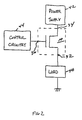
- Fig. 2 illustrates transistor 10 of Fig. 1 connected in a high side driver configuration.
- the drain contact 34 is connected to power supply 42.
- the gate contact 36 is connected to control circuitry 44 and the source contact 32 is connected to load 46.
- RESURF LDMOS transistor 10 of Fig. 1 operates in the following manner under normal conditions.
- V t the device threshold voltage
- the channel 30 conducts and current flows from the drain contact 34, through the drain contact diffusion 16, through the drain drift region 14, through the second drain contact diffusion 18, through the polysilicon drain interconnect 26a, through the polysilicon channel 30, through the polysilicon source 26b, and finally through the source contact 32.
- V t the device threshold voltage
- the polysilicon channel 30 does not conduct and the transistor 10 behaves like an open circuit.
- RESURF LDMOS transistor 10 of Fig. 1 advantageously operates in a manner such that the power transistor's reliability is not compromised during breakdown conditions.
- the breakdown voltage magnitude of a RESURF LDMOS transistor is a complex function of the drain drift region 14 length, depth, and doping concentration; breakdown voltage ratings may vary widely, from 40-500V.
- the drain contact 34 is coupled to the power supply and therefore the transient voltage appears on the drain contact 34.
- the drain drift region 14 of the transistor 10 becomes fully depleted. Most of the voltage drop occurs across the drain drift region 14 such that only 5-10 volts will drop across the source isolated, embedded gate NMOS transistor 40.
- the drain drift region 14 becomes fully depleted, the junction between the drain drift region 14 and substrate 12 breaks down. Since the breakdown site is well within the bulk of substrate 12, no charge is injected into surface oxides 24a thereby prohibiting unstable or walking breakdown phenomena.
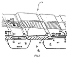
- Fig. 3 is a three dimensional drawing illustrating an alternative embodiment of the invention.
- RESURF LDMOS transistor 10 the drain interconnect 26a extends over the insulating layer 24b and forms a MOS gated drift region 26a.
- This alternative embodiment provides improved RDSon ("on" resistance) through use of the MOS gated drift region 26a.
- the insulating layer 24b formed over the drain drift region 14 has a minimum thickness dictated by the breakdown voltage required by the design application. This is required because the voltage drop across the insulating layer 24b near the drain contact diffusion 16 will approximate the breakdown voltage. As applications require an increased breakdown voltage the insulating layer 24b thickness over the drain drift region 14 must also increase to prevent the insulating layer 24b form breaking down.
Abstract
Description
- This invention is in the field of semiconductor integrated circuits and relates primarily to high power devices.
- In the field of power integrated circuits much work has been done in the development of power transistors. Advancements were made enabling LDMOS power transistors (lateral double diffused MOS transistor) to exhibit low "on-resistance" (RDSon) and high breakdown capability concurrently through a reduced surface field (RESURF) technique (J.A. Appels and H.M.J. Vaes, "High Voltage Thin Layer Devices (RESURF Devices)", IEDM Tech. Digest, pp. 238-241, 1979).
- In the past, RESURF LDMOS transistors commonly were used in low side driver applications because the transistor structure coupled the source to the substrate which in turn was coupled to ground. (A low side driver configuration consists of the source of the LDMOS transistor coupled to ground and the drain coupled to an output load.) Therefore, RESURF LDMOS transistors were not utilized in high side driver applications and other applications that mandated electrical isolation between the source and substrate. (A high side driver configuration consists of the LDMOS transistor drain coupled to circuitry or a power supply and the source coupled to an output load.)
- It is an object of this invention to provide a high power integrated circuit device with electrical isolation between source and substrate. It is another object of this invention to provide a LDMOS transistor with an isolated source and RESURF drift region. Other objects and advantages of the invention will become apparent to those of ordinary skill in the art having reference to the following specification together with the drawings herein.
- An integrated circuit RESURF LDMOS power transistor combines a source isolated, embedded gate MOS transistor with RESURF LDMOS technology to provide a source isolated high voltage power transistor with low "on" resistance for use in applications where the source is required to be electrically isolated from the substrate.
- Reference will now be made, by way of example, to the accompanying drawings, in which:
- Figure 1 is a three dimensional drawing illustrating the preferred embodiment of the invention;
- Figure 2 is a block diagram illustrating a high side driver circuit configuration; and
- Figure 3 is a three dimensional drawing illustrating an alternative embodiment of the invention.
- Fig. 1 is a cross section drawing illustrating the preferred embodiment of the invention. A RESURF LDMOS transistor 10 has a
P type substrate 12. A patternedoxide layer 24a is formed over the face of thesubstrate 12 using a standard LOCOS process with two openings provided for implants. An implant forms an N- typedrain drift region 14 and an N- typegate isolation region 20 in theP type substrate 12. A patterned oxide layer 24b is formed over thedrain drift region 14 with an opening separating thethick oxide 24a overlying thesubstrate 12 and the oxide 24b overlying thedrain drift region 14. A P type doped polysilicon layer 30 is formed over theoxide layers 24a and 24b and forms the channel 30 of the transistor 10. The P type polysilicon layer 30 is etched to remove a portion of the polysilicon lying over the oxide layer 24b. A photoresist is deposited over a portion of the P type poly channel 30 overlying the gate isolation region while an N+ type implant dopes the remaining portion of the poly layer. The N+ type implant forms N+type contact diffusions 16 and 18 in thedrain drift region 14. This process step also forms an N+type drain interconnect 26a which connects thedrain drift region 14 through contact diffusion 18 to the channel 30 and anN+ type source 26b formed on the other side of the poly channel 30. The photoresist is then removed. A patterned oxide layer (not shown in Fig. 1) is formed over the transistor 10 with holes opened for the formation of metal contacts. A patterned metal layer is formed over the transistor 10 forming asource contact 32, agate contact 36, and adrain contact 34. - The invention illustrated in Fig. 1 provides a source isolated (
source 26b electrically isolated from the substrate 12), embedded gate NMOS transistor 40 coupled to a RESURFdrain drift region 14 to form a RESURF LDMOS transistor 10 for use in applications mandating electrical isolation between thesource 26b andsubstrate 12. The source isolated, embedded gate NMOS transistor 40 is constructed upside-down with respect to a conventional NMOS transistor construction in thesubstrate 12. TheN+ type diffusion 22 serves as the gate of the transistor 40 and the thin portion ofinsulating layer 24a overlyinggate region 22 serves as a gate oxide for the transistor 40. The channel 30, on top of the insulating layer 24, completes the upside-down transistor 40 construction. The gate oxide is high quality since it is formed over gate diffusion 22 (diffusions made in a single crystal silicon substrate become single crystal silicon diffusions). The single crystalsilicon gate diffusion 22 allows the gate oxide to be very thin thus maximizing current drive which is well known by those skilled in the art. This is also readily seen in the current equation for an NMOS transistor (for W/L = unity):

The gate oxide thickness (tox) is located in the denominator of the equation and is therefore inversely proportional to the current drive capability (ID). Thus, the thinner the gate oxide (tox) can be made the better the current drive of the transistor will become. - Fig. 2 illustrates transistor 10 of Fig. 1 connected in a high side driver configuration. The
drain contact 34 is connected topower supply 42. Thegate contact 36 is connected tocontrol circuitry 44 and thesource contact 32 is connected toload 46. - RESURF LDMOS transistor 10 of Fig. 1 operates in the following manner under normal conditions. When a positive voltage greater in magnitude than the device threshold voltage (Vt, usually 1-2V) appears on the
transistor gate contact 36 the channel 30 conducts and current flows from thedrain contact 34, through thedrain contact diffusion 16, through thedrain drift region 14, through the second drain contact diffusion 18, through the polysilicon drain interconnect 26a, through the polysilicon channel 30, through thepolysilicon source 26b, and finally through thesource contact 32. When a voltage lower than the device threshold voltage appears on thetransistor gate contact 36 the polysilicon channel 30 does not conduct and the transistor 10 behaves like an open circuit. - RESURF LDMOS transistor 10 of Fig. 1 advantageously operates in a manner such that the power transistor's reliability is not compromised during breakdown conditions. (The breakdown voltage magnitude of a RESURF LDMOS transistor is a complex function of the
drain drift region 14 length, depth, and doping concentration; breakdown voltage ratings may vary widely, from 40-500V.) During a power supply transient thedrain contact 34 is coupled to the power supply and therefore the transient voltage appears on thedrain contact 34. When a transient voltage appears at thedrain contact 34 that exceeds the transistor 10 breakdown rating, thedrain drift region 14 of the transistor 10 becomes fully depleted. Most of the voltage drop occurs across thedrain drift region 14 such that only 5-10 volts will drop across the source isolated, embedded gate NMOS transistor 40. When thedrain drift region 14 becomes fully depleted, the junction between thedrain drift region 14 andsubstrate 12 breaks down. Since the breakdown site is well within the bulk ofsubstrate 12, no charge is injected intosurface oxides 24a thereby prohibiting unstable or walking breakdown phenomena. - Fig. 3 is a three dimensional drawing illustrating an alternative embodiment of the invention. In this embodiment, RESURF LDMOS transistor 10 the
drain interconnect 26a extends over the insulating layer 24b and forms a MOSgated drift region 26a. This alternative embodiment provides improved RDSon ("on" resistance) through use of the MOSgated drift region 26a. - In Fig. 3 during a breakdown condition, the majority of voltage drops across
drain drift region 14 thus causing the voltage drop across the source isolated, embedded gate transistor 40 (MOSgated drift region 26a, channel 30 andsource 26b) to be approximately 5-10 volts. The existence of this voltage on the MOSgated drift region 26a creates a negative voltage on the MOSgated drift region 26a relative to the voltage in thedrain drift region 14 and therefore makes the MOSgated drift region 26a, lying over the first insulating layer 24b, operate as a field plate, thus pushing electrons in thedrain drift region 14 down toward thesubstrate 12. This causes thedrain drift region 14 to deplete in two directions, from the substrate 12-drain drift region 14 junction up towards the insulating layer 24b and from the drain drift region 14-insulating layer 24b junction down towards thesubstrate 12. This "top and bottom" dual depletion condition allows thedrain drift region 14 to be doped more heavily during processing to further improve RDSon performance. RDSon is reduced when the transistor 10 is operating in the "on" mode and therefore the transistor 10 more accurately simulates an ideal switch. - The insulating layer 24b formed over the
drain drift region 14 has a minimum thickness dictated by the breakdown voltage required by the design application. This is required because the voltage drop across the insulating layer 24b near thedrain contact diffusion 16 will approximate the breakdown voltage. As applications require an increased breakdown voltage the insulating layer 24b thickness over thedrain drift region 14 must also increase to prevent the insulating layer 24b form breaking down. - Although the invention has been described with reference to the preferred embodiment herein, this description is not to be construed in a limiting sense. Various modifications of the disclosed embodiment, such as modifications to drain
drift region 14 length, depth or doping concentration, as well as other embodiments of the invention, will become apparent to persons skilled in the art upon reference to the description of the invention. It is therefore contemplated that the appended claims will cover any such modifications or embodiments as fall within the true scope of the invention.
Claims (15)
- A high voltage power transistor, comprising:
a source isolated, embedded gate MOS transistor;
a bulk semiconductor drain drift region connected to the source isolated, embedded gate MOS transistor. - The high voltage power transistor of claim 1, wherein the source isolated, embedded gate MOS transistor comprises:
a substrate of semiconductor material;
a diffusion formed in the substrate whereby a gate isolation diffusion is formed;
a second diffusion of higher doping concentration than the gate isolation diffusion formed in the gate isolation diffusion whereby a gate diffusion is formed;
an insulating layer overlying the source isolated, embedded gate transistor whereby a gate oxide is formed over the gate diffusion; and
a semiconductor layer deposited over the insulating layer having three sections, one section forming a source for both the source isolated, embedded gate MOS transistor and the high voltage power transistor, a second section forming a channel, and a third section forming a drain. - The high voltage power transistor of claim 2, wherein the substrate and the channel are composed of P type semiconductor material, the gate isolation diffusion is composed of N- type semiconductor material, and the gate diffusion, source, and drain are composed of N+ type semiconductor material.
- The high voltage power transistor of claim 2 or claim 3, wherein the substrate, gate isolation diffusion, gate diffusion, and semiconductor layer having three sections are composed of single crystal silicon.
- The high voltage power transistor of any of claims 2 to 4, wherein the semiconductor layer having three sections is composed of polycrystalline silicon.
- The high voltage power transistor of any if claims 2 to 5, wherein the insulating layer overlying the substrate is either silicon dioxide, silicon nitride, or a combination of silicon dioxide and silicon nitride.
- The high voltage power transistor of any preceding claim, wherein the drain drift region comprises:
a substrate of semiconductor material;
a diffusion in the substrate whereby a drift region is formed;
a first diffusion, inside the drift region, of higher doping concentration than the drift region whereby a drain contact region is formed;
a second diffusion, spaced from the first diffusion and inside the drift region, of higher doping concentration than the drift region whereby a drain drift region contact is formed;
a patterned insulating layer overlying the drain drift region with openings for contact down to the first and second diffusions inside the drift region; and
a patterned conductive layer making electrical contact to both the second diffusion inside the drift region and to a drain of the source isolated, embedded gate transistor. - The high voltage power transistor of claim 7, wherein the patterned conductive layer overlying the patterned insulating layer comprises two sections, one section making said electrical contact to both the second diffusion inside the drift region and to the drain of the source isolated, embedded gate transistor, and a second section lying between the first and second diffusions inside the drift region whereby a field plate is formed.
- The high voltage power transistor of claim 7 or claim 8, wherein the conductive layer is electrically connected to either source, gate, or drain terminal of the source isolated, embedded gate transistor, or is held at a potential below that of the drain terminal of the high voltage power device.
- The high voltage power transistor of any of claims 7 to 9, wherein the substrate is P type semiconductor material, the drift region is N type semiconductor material, and both first and second diffusions inside the drift region are N+ type semiconductor material.
- The high voltage power transistor of any of claims 8 to 10, wherein the P type substrate doping concentration and the N type drift region depth and doping profile are designed according to RESURF design principles such that the drift region fully depletes at or before rated breakdown voltage of the high voltage power transistor.
- A high voltage power transistor with electrical isolation between source and substrate, comprising:
a drain drift region formed in a semiconductor substrate having a drain contact and an interconnect contact; and
a source isolated, embedded gate MOS transistor formed on an insulating layer overlying the substrate, having a source contact, a gate contact, and a drain interconnect connected to the interconnect contact of the drain drift region. - A high side driver configuration with a high voltage power transistor having its source isolated from the substrate, comprising:
a drain drift region formed in a semiconductor substrate having a drain contact and an interconnect contact with the drain contact connected to a power supply; and
a source isolated, embedded gate MOS transistor having a source contact, a gate contact, and a drain interconnect, with the source contact connected to a load, the gate contact connected to control circuitry, and the drain interconnect connected to the interconnect contact of the drain drift region. - A method of forming a high voltage power transistor, comprising:
forming a source isolated, embedded gate MOS transistor; and
forming a drain drift region connected to the source isolated, embedded gate MOS transistor. - A method of configuring a high voltage power transistor in a high side driver configuration, comprising:
forming a drain drift region in a semiconductor substrate having a drain contact and an interconnect contact with the drain contact connected to a power supply; and
forming a source isolated, embedded gate MOS transistor having a source contact, a gate contact, and a drain interconnect with the source contact connected to a load, the gate contact connected to control circuitry, and the drain interconnect connected to the interconnect contact of the drain drift region.
Applications Claiming Priority (2)
| Application Number | Priority Date | Filing Date | Title |
|---|---|---|---|
| US85786192A | 1992-03-26 | 1992-03-26 | |
| US857861 | 1992-03-26 |
Publications (3)
| Publication Number | Publication Date |
|---|---|
| EP0562352A2 true EP0562352A2 (en) | 1993-09-29 |
| EP0562352A3 EP0562352A3 (en) | 1994-01-05 |
| EP0562352B1 EP0562352B1 (en) | 1998-02-18 |
Family
ID=25326881
Family Applications (1)
| Application Number | Title | Priority Date | Filing Date |
|---|---|---|---|
| EP93103748A Expired - Lifetime EP0562352B1 (en) | 1992-03-26 | 1993-03-09 | High voltage structures with oxide isolated source and RESURF drift region in bulk silicon |
Country Status (5)
| Country | Link |
|---|---|
| US (1) | US5350932A (en) |
| EP (1) | EP0562352B1 (en) |
| JP (1) | JP3393149B2 (en) |
| KR (1) | KR100301917B1 (en) |
| DE (1) | DE69317004T2 (en) |
Cited By (1)
| Publication number | Priority date | Publication date | Assignee | Title |
|---|---|---|---|---|
| US6087232A (en) * | 1997-10-28 | 2000-07-11 | Electronics And Telecommunications Research Institute | Fabrication method of lateral double diffused MOS transistors |
Families Citing this family (14)
| Publication number | Priority date | Publication date | Assignee | Title |
|---|---|---|---|---|
| US5510275A (en) * | 1993-11-29 | 1996-04-23 | Texas Instruments Incorporated | Method of making a semiconductor device with a composite drift region composed of a substrate and a second semiconductor material |
| US5777363A (en) * | 1993-11-29 | 1998-07-07 | Texas Instruments Incorporated | Semiconductor device with composite drift region |
| US6831331B2 (en) | 1995-11-15 | 2004-12-14 | Denso Corporation | Power MOS transistor for absorbing surge current |
| US6242787B1 (en) | 1995-11-15 | 2001-06-05 | Denso Corporation | Semiconductor device and manufacturing method thereof |
| US5920097A (en) * | 1997-03-26 | 1999-07-06 | Advanced Micro Devices, Inc. | Compact, dual-transistor integrated circuit |
| US6545316B1 (en) | 2000-06-23 | 2003-04-08 | Silicon Wireless Corporation | MOSFET devices having linear transfer characteristics when operating in velocity saturation mode and methods of forming and operating same |
| US6621121B2 (en) | 1998-10-26 | 2003-09-16 | Silicon Semiconductor Corporation | Vertical MOSFETs having trench-based gate electrodes within deeper trench-based source electrodes |
| US6236100B1 (en) * | 2000-01-28 | 2001-05-22 | General Electronics Applications, Inc. | Semiconductor with high-voltage components and low-voltage components on a shared die |
| US6784486B2 (en) * | 2000-06-23 | 2004-08-31 | Silicon Semiconductor Corporation | Vertical power devices having retrograded-doped transition regions therein |
| US6781194B2 (en) * | 2001-04-11 | 2004-08-24 | Silicon Semiconductor Corporation | Vertical power devices having retrograded-doped transition regions and insulated trench-based electrodes therein |
| JP3831598B2 (en) * | 2000-10-19 | 2006-10-11 | 三洋電機株式会社 | Semiconductor device and manufacturing method thereof |
| US20030091556A1 (en) * | 2000-12-04 | 2003-05-15 | Ruoslahti Erkki I. | Methods of inhibiting tumor growth and angiogenesis with anastellin |
| WO2002084745A2 (en) * | 2001-04-11 | 2002-10-24 | Silicon Wireless Corporation | Power semiconductor devices and methods of forming same |
| JP4618629B2 (en) * | 2004-04-21 | 2011-01-26 | 三菱電機株式会社 | Dielectric isolation type semiconductor device |
Citations (6)
| Publication number | Priority date | Publication date | Assignee | Title |
|---|---|---|---|---|
| JPS587870A (en) * | 1981-07-07 | 1983-01-17 | Toshiba Corp | Semiconductor integrated circuit device |
| EP0073487A2 (en) * | 1981-08-31 | 1983-03-09 | Kabushiki Kaisha Toshiba | Method for manufacturing three-dimensional semiconductor device |
| JPS59145560A (en) * | 1983-02-09 | 1984-08-21 | Matsushita Electronics Corp | Output buffer device |
| JPS60163451A (en) * | 1984-02-03 | 1985-08-26 | Seiko Epson Corp | Output protection circuit |
| JPS62101067A (en) * | 1985-10-28 | 1987-05-11 | Nec Corp | Input protecting device |
| EP0312955A2 (en) * | 1987-10-15 | 1989-04-26 | Nec Corporation | Semiconductor device having an improved thin film transistor |
Family Cites Families (3)
| Publication number | Priority date | Publication date | Assignee | Title |
|---|---|---|---|---|
| US4752814A (en) * | 1984-03-12 | 1988-06-21 | Xerox Corporation | High voltage thin film transistor |
| EP0333426B1 (en) * | 1988-03-15 | 1996-07-10 | Kabushiki Kaisha Toshiba | Dynamic RAM |
| JPH03147362A (en) * | 1989-11-01 | 1991-06-24 | Seiko Epson Corp | Semiconductor |
-
1993
- 1993-03-09 DE DE69317004T patent/DE69317004T2/en not_active Expired - Fee Related
- 1993-03-09 EP EP93103748A patent/EP0562352B1/en not_active Expired - Lifetime
- 1993-03-25 KR KR1019930004648A patent/KR100301917B1/en not_active IP Right Cessation
- 1993-03-26 JP JP06813793A patent/JP3393149B2/en not_active Expired - Fee Related
- 1993-12-17 US US08/169,731 patent/US5350932A/en not_active Expired - Lifetime
Patent Citations (6)
| Publication number | Priority date | Publication date | Assignee | Title |
|---|---|---|---|---|
| JPS587870A (en) * | 1981-07-07 | 1983-01-17 | Toshiba Corp | Semiconductor integrated circuit device |
| EP0073487A2 (en) * | 1981-08-31 | 1983-03-09 | Kabushiki Kaisha Toshiba | Method for manufacturing three-dimensional semiconductor device |
| JPS59145560A (en) * | 1983-02-09 | 1984-08-21 | Matsushita Electronics Corp | Output buffer device |
| JPS60163451A (en) * | 1984-02-03 | 1985-08-26 | Seiko Epson Corp | Output protection circuit |
| JPS62101067A (en) * | 1985-10-28 | 1987-05-11 | Nec Corp | Input protecting device |
| EP0312955A2 (en) * | 1987-10-15 | 1989-04-26 | Nec Corporation | Semiconductor device having an improved thin film transistor |
Non-Patent Citations (6)
| Title |
|---|
| INTERNATIONAL ELECTRON DEVICES MEETING 1979 WASHINTON, D.C. DECEMBER 3-4-5 TECHNICAL DIGEST pages 370 - 373 T. LIZUKA ET AL 'VARIABLE RESISTANCE POLYSILICON FOR HIGH DENSITY CMOS RAM' * |
| JAPANESE JOURNAL OF APPLIED PHYSICS, SUPPLEMENTS 1991 , TOKYO JA pages 174 - 176 H. KITAJIMA ET AL 'Leakage Current Reduction in Sub-Micron Channel Poly-Si TFTs' * |
| PATENT ABSTRACTS OF JAPAN vol. 007, no. 080 (E-168)2 April 1983 & JP-A-58 007 870 (TOKYO SHIBAURA DENKI KK) 17 January 1983 * |
| PATENT ABSTRACTS OF JAPAN vol. 008, no. 277 (E-285)18 December 1984 & JP-A-59 145 560 (MARSUSHITA DENSHI KOGYO KK) 21 August 1984 * |
| PATENT ABSTRACTS OF JAPAN vol. 011, no. 309 (E-547)8 October 1987 & JP-A-62 101 067 (NEC CORP) 11 May 1987 * |
| PATENT ABSTRACTS OF JAPAN vol. 9, no. 332 (E-370)(2055) 26 December 1985 & JP-A-60 163 451 (SUWA SEIKOSHA K.K.) 26 August 1985 * |
Cited By (1)
| Publication number | Priority date | Publication date | Assignee | Title |
|---|---|---|---|---|
| US6087232A (en) * | 1997-10-28 | 2000-07-11 | Electronics And Telecommunications Research Institute | Fabrication method of lateral double diffused MOS transistors |
Also Published As
| Publication number | Publication date |
|---|---|
| JP3393149B2 (en) | 2003-04-07 |
| DE69317004D1 (en) | 1998-03-26 |
| EP0562352A3 (en) | 1994-01-05 |
| KR100301917B1 (en) | 2001-10-22 |
| KR930020738A (en) | 1993-10-20 |
| JPH06283715A (en) | 1994-10-07 |
| DE69317004T2 (en) | 1998-06-10 |
| US5350932A (en) | 1994-09-27 |
| EP0562352B1 (en) | 1998-02-18 |
Similar Documents
| Publication | Publication Date | Title |
|---|---|---|
| EP0562271B1 (en) | High voltage structure with oxide isolated source and resurf drift region in bulk silicon | |
| US5539238A (en) | Area efficient high voltage Mosfets with vertical resurf drift regions | |
| US5723891A (en) | Top-drain trench based resurf DMOS transistor structure | |
| US5274259A (en) | High voltage transistor | |
| EP0788660B1 (en) | Semiconductor device of hv-ldmost type | |
| CA2040396C (en) | Semiconductor device with reduced time-dependent dielectric failures | |
| US6781195B2 (en) | Semiconductor bidirectional switching device and method | |
| US5350932A (en) | High voltage structures with oxide isolated source and resurf drift region in bulk silicon | |
| EP0110331B1 (en) | A mos transistor | |
| JPH0656888B2 (en) | Semiconductor device | |
| JPH0823098A (en) | Bidirectional current blocking mosfet and reduction of on-resistance of bidirectional current blocking mosfet | |
| US5072267A (en) | Complementary field effect transistor | |
| US7888768B2 (en) | Power integrated circuit device having embedded high-side power switch | |
| US20080087949A1 (en) | Semiconductor device and method of manufacturing the same | |
| EP0557126A1 (en) | Power semiconductor device | |
| US5596216A (en) | Semiconductor device with diode and capable of device protection | |
| US6188111B1 (en) | Dual gate semiconductor device for shortening channel length | |
| US6180983B1 (en) | High-voltage MOS transistor on a silicon on insulator wafer | |
| US5627385A (en) | Lateral silicon carbide transistor | |
| EP0654827A1 (en) | Integrated power cascode | |
| JPH10107269A (en) | Semiconductor device controllable by field effect and its manufacture | |
| US11677033B2 (en) | Passive element on a semiconductor base body | |
| JPH0760901B2 (en) | Semiconductor device | |
| JPH02106973A (en) | Semiconductor device |
Legal Events
| Date | Code | Title | Description |
|---|---|---|---|
| PUAI | Public reference made under article 153(3) epc to a published international application that has entered the european phase |
Free format text: ORIGINAL CODE: 0009012 |
|
| AK | Designated contracting states |
Kind code of ref document: A2 Designated state(s): DE FR GB IT NL |
|
| PUAL | Search report despatched |
Free format text: ORIGINAL CODE: 0009013 |
|
| AK | Designated contracting states |
Kind code of ref document: A3 Designated state(s): DE FR GB IT NL |
|
| 17P | Request for examination filed |
Effective date: 19940916 |
|
| 17Q | First examination report despatched |
Effective date: 19960318 |
|
| GRAG | Despatch of communication of intention to grant |
Free format text: ORIGINAL CODE: EPIDOS AGRA |
|
| GRAG | Despatch of communication of intention to grant |
Free format text: ORIGINAL CODE: EPIDOS AGRA |
|
| GRAH | Despatch of communication of intention to grant a patent |
Free format text: ORIGINAL CODE: EPIDOS IGRA |
|
| GRAH | Despatch of communication of intention to grant a patent |
Free format text: ORIGINAL CODE: EPIDOS IGRA |
|
| GRAA | (expected) grant |
Free format text: ORIGINAL CODE: 0009210 |
|
| ITF | It: translation for a ep patent filed |
Owner name: BARZANO' E ZANARDO ROMA S.P.A. |
|
| AK | Designated contracting states |
Kind code of ref document: B1 Designated state(s): DE FR GB IT NL |
|
| REF | Corresponds to: |
Ref document number: 69317004 Country of ref document: DE Date of ref document: 19980326 |
|
| ET | Fr: translation filed | ||
| PGFP | Annual fee paid to national office [announced via postgrant information from national office to epo] |
Ref country code: NL Payment date: 19980430 Year of fee payment: 6 |
|
| PLBE | No opposition filed within time limit |
Free format text: ORIGINAL CODE: 0009261 |
|
| STAA | Information on the status of an ep patent application or granted ep patent |
Free format text: STATUS: NO OPPOSITION FILED WITHIN TIME LIMIT |
|
| 26N | No opposition filed | ||
| PG25 | Lapsed in a contracting state [announced via postgrant information from national office to epo] |
Ref country code: NL Free format text: LAPSE BECAUSE OF NON-PAYMENT OF DUE FEES Effective date: 19991001 |
|
| NLV4 | Nl: lapsed or anulled due to non-payment of the annual fee |
Effective date: 19991001 |
|
| REG | Reference to a national code |
Ref country code: GB Ref legal event code: IF02 |
|
| PGFP | Annual fee paid to national office [announced via postgrant information from national office to epo] |
Ref country code: IT Payment date: 20070628 Year of fee payment: 15 |
|
| PGFP | Annual fee paid to national office [announced via postgrant information from national office to epo] |
Ref country code: GB Payment date: 20080211 Year of fee payment: 16 |
|
| PGFP | Annual fee paid to national office [announced via postgrant information from national office to epo] |
Ref country code: FR Payment date: 20080307 Year of fee payment: 16 Ref country code: DE Payment date: 20080331 Year of fee payment: 16 |
|
| PG25 | Lapsed in a contracting state [announced via postgrant information from national office to epo] |
Ref country code: IT Free format text: LAPSE BECAUSE OF NON-PAYMENT OF DUE FEES Effective date: 20080309 |
|
| GBPC | Gb: european patent ceased through non-payment of renewal fee |
Effective date: 20090309 |
|
| REG | Reference to a national code |
Ref country code: FR Ref legal event code: ST Effective date: 20091130 |
|
| PG25 | Lapsed in a contracting state [announced via postgrant information from national office to epo] |
Ref country code: DE Free format text: LAPSE BECAUSE OF NON-PAYMENT OF DUE FEES Effective date: 20091001 |
|
| PG25 | Lapsed in a contracting state [announced via postgrant information from national office to epo] |
Ref country code: GB Free format text: LAPSE BECAUSE OF NON-PAYMENT OF DUE FEES Effective date: 20090309 Ref country code: FR Free format text: LAPSE BECAUSE OF NON-PAYMENT OF DUE FEES Effective date: 20091123 |