EP0557032B1 - Pulse-width modulator for class D amplifier - Google Patents
Pulse-width modulator for class D amplifier Download PDFInfo
- Publication number
- EP0557032B1 EP0557032B1 EP93301064A EP93301064A EP0557032B1 EP 0557032 B1 EP0557032 B1 EP 0557032B1 EP 93301064 A EP93301064 A EP 93301064A EP 93301064 A EP93301064 A EP 93301064A EP 0557032 B1 EP0557032 B1 EP 0557032B1
- Authority
- EP
- European Patent Office
- Prior art keywords
- coupled
- voltage
- amplifier
- input
- hysteresis
- Prior art date
- Legal status (The legal status is an assumption and is not a legal conclusion. Google has not performed a legal analysis and makes no representation as to the accuracy of the status listed.)
- Expired - Lifetime
Links
- 230000008878 coupling Effects 0.000 claims description 15
- 238000010168 coupling process Methods 0.000 claims description 15
- 238000005859 coupling reaction Methods 0.000 claims description 15
- 239000003990 capacitor Substances 0.000 description 33
- 239000004020 conductor Substances 0.000 description 7
- 238000010586 diagram Methods 0.000 description 6
- 230000001105 regulatory effect Effects 0.000 description 4
- 239000004065 semiconductor Substances 0.000 description 4
- 238000013459 approach Methods 0.000 description 2
- 238000004519 manufacturing process Methods 0.000 description 2
- 230000037361 pathway Effects 0.000 description 2
- 239000011324 bead Substances 0.000 description 1
- 239000000969 carrier Substances 0.000 description 1
- 230000008859 change Effects 0.000 description 1
- 230000001447 compensatory effect Effects 0.000 description 1
- 230000000295 complement effect Effects 0.000 description 1
- 238000013016 damping Methods 0.000 description 1
- 230000007812 deficiency Effects 0.000 description 1
- 238000007599 discharging Methods 0.000 description 1
- 238000005516 engineering process Methods 0.000 description 1
- 239000000463 material Substances 0.000 description 1
- 230000035699 permeability Effects 0.000 description 1
- 238000011084 recovery Methods 0.000 description 1
Images

Classifications
-
- H—ELECTRICITY
- H03—ELECTRONIC CIRCUITRY
- H03F—AMPLIFIERS
- H03F3/00—Amplifiers with only discharge tubes or only semiconductor devices as amplifying elements
- H03F3/20—Power amplifiers, e.g. Class B amplifiers, Class C amplifiers
- H03F3/21—Power amplifiers, e.g. Class B amplifiers, Class C amplifiers with semiconductor devices only
- H03F3/217—Class D power amplifiers; Switching amplifiers
- H03F3/2171—Class D power amplifiers; Switching amplifiers with field-effect devices
Definitions
- This invention relates to improved class D amplifiers. It is disclosed in the context of a class D audio amplifier, but is believed to have applicability to class D amplifiers for other applications as well.
- hysteresis pulse width modulators In class D audio amplifier design, hysteresis pulse width modulators have the inherent advantages of low distortion, high power supply rejection, and automatic compensation for any switching waveform anomalies caused by non-ideal components.
- the operating frequency of circuits employing class D technology varies dramatically with input signal voltage.
- a hysteresis-type pulse width modulator converts an input voltage into a pulse width modulated waveform, the width of the pulses of which is related to the input voltage amplitude.
- the modulator comprises a window comparator, a supply voltage source having a pair of terminals across which a supply voltage is provided, and a hysteresis voltage source having a pair of terminals across which a hysteresis voltage is provided.
- the hysteresis voltage source comprises a multiplier, a comparator for adding the supply voltage and input voltage to generate a sum voltage, and a comparator for subtracting the input voltage from the supply voltage to generate a difference voltage.
- the hysteresis-type pulse width modulator comprises an integrator, the window comparator, the hysteresis voltage source, and a flip-flop.
- the input voltage is coupled to the integrator, the integrator to the window comparator, the window comparator to the flip-flop, and the hysteresis voltage source to the window comparator.
- the window comparator comprises first and second comparators, each having non-inverting and inverting terminals.
- the integrator is coupled to the window comparator by coupling an output terminal of the integrator to a non-inverting input terminal of the first comparator and to an inverting input terminal of the second comparator.
- the hysteresis voltage source is coupled to the window comparator by coupling a first of the pair of terminals of the hysteresis voltage source to the inverting input terminal of the first comparator and a second of the pair of terminals of the hysteresis voltage source to the non-inverting input terminal of the second comparator.
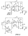
- a difference amplifier 10 which illustratively is one-half of a National Semiconductor LM833, is coupled in integrator amplifier configuration to receive at its inverting (-) input terminal the input voltage signal V i through an input resistor 12.
- the non-inverting input terminal (+) of difference amplifier 10 is coupled to ground.
- An integrating capacitor 14 is coupled across the output terminal and - input terminal of amplifier 10.
- the output terminal of amplifier 10 is coupled to the + input terminal and - input terminal, respectively, of two difference amplifiers 16 and 18.
- the - input terminal of amplifier 16 is coupled to one terminal of a hysteresis voltage source 20 (illustrated as a battery) which provides a constant output voltage V h .
- the other terminal of source 20 is coupled to the + input terminal of amplifier 18, and to ground.
- Difference amplifiers 16, 18 illustratively are each one-half of a National Semiconductor LM319.
- the coupling of difference amplifiers 16, 18 in this configuration constitutes a window comparator 22, the output terminals 24, 26 of which provide positive-going pulses at the S and R input terminals, respectively, of an SR flip-flop 28, depending upon whether the output signal from amplifier 10 is above V h or below ground, respectively.
- the Q output terminal of flip-flop 28 provides the modulated width pulses of the pulse width modulator 30 of Fig. 1.
- Flip-flop 28 illustratively is half of an RCA CD4011 quad NAND gate.
- a class D audio amplifier these signals are then supplied to a basic, or power, amplifier 32, the output of which is supplied through a low pass filter including an inductor 34 in series and a capacitor 36 in parallel with a primarily resistive load 38, which illustratively is the voice coil of a moving coil loudspeaker.
- Feedback customarily is provided from an output terminal of power amplifier 32 to the - input terminal of amplifier 10 through a feedback resistor 39.
- the pulse width modulator 30's own reduced operating frequency f pwm can pass though the low pass filter 34, 36 and appear in the audio output of transducer 38.
- the hysteresis voltage, V h is made to vary in a compensatory manner with V i so that the pulse width modulator 30's operating frequency f pwm remains constant throughout the range of input voltage V i .
- Inputs to the multiplier are K(V s -V i ) and K(V s +V i ) which are readily available.
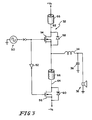
- a hysteresis voltage (V h ') supply 42 includes first 44 and second 46 difference amplifiers and a multiplier 48.
- the input voltage V i is coupled to the + input terminal of the first difference amplifier 44 and to the - input terminal of the second difference amplifier 46.
- the - input terminal of first difference amplifier 44 is coupled the -V, terminal.
- the + input terminal of second difference amplifier 46 is coupled to the +V s terminal.
- the signals at the output terminals of difference amplifiers 44, 46 are thus K(V s + V i ) and K(V s - V i ), respectively, where K is a constant, the gain of amplifiers 44, 46.
- These signals are coupled to two input terminals of multiplier 48 to provide the K 2 (V s - V i ) (V s + V i ) or V h ' hysteresis voltage signal required by equation (3) to the window comparator 22.
- the operating frequency f pwm of the pulse width modulator 40 has thus been rendered a constant, insensitive to the input voltage V i .
- Amplifiers 44, 46 and multiplier 48 illustratively are collectively realized by a ROHM BA6110 operational transconductance amplifier.
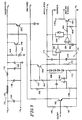
- a basic amplifier 32 receives appropriately preamplified and otherwise processed signals from a logic drive source 50 which includes SR flip-flop 28 of Figs. 1-2.
- the driver stage of amplifier 32 includes a final driver inverting amplifier 52 and a pair of output MOSFET switches 54, 56.
- Switches 54, 56 illustratively are Motorola MTP 50N06E MOSFETs. Switches 54, 56 are coupled in push pull configuration, with the inverting amplifier 52 inverting the signal which is coupled to the gate of switch 54 and providing this inverted drive signal to the gate of switch 56.
- Each switch 54, 56 is provided with a body diode 58, 60, respectively.
- Diodes 58, 60 are formed on the material from which switches 54, 56 are fabricated at the time of fabrication of the switches 54, 56 so that devices 54, 58 are in the same package and devices 56, 60 are in the same package and there are no external leads between devices 54, 58 or between devices 56, 60.
- the drain lead of MOSFET 54 and cathode of diode 58 are coupled by a suitable conductor 62 to the +V s supply terminal.
- the source lead of MOSFET 54 and anode of diode 58 are coupled through the series inductor 34 to the parallel combination of capacitor 36 and load 38.
- the source lead of MOSFET 54 and anode of diode 58 are also coupled to the drain lead of MOSFET 56 and cathode of diode 60 by a suitable conductor 64.
- the source lead of MOSFET 56 and anode of diode 60 are coupled to the -V s supply terminal.
- a high magnetic permeability bead 66 is placed on each of conductors 62, 64.
- the various illustrated pin numbers on the illustrated integrated circuits and devices refer to the specific integrated circuits and devices which have already been identified or will be identified herein. However, that does not constitute a representation, nor should any such representation be inferred, that there are no integrated circuits or devices other than those identified herein that will perform the functions performed by the identified integrated circuits and devices.
- V i Common mode noise rejection in the input signal V i is achieved by an input difference amplifier 80 which illustratively is one half of a National Semiconductor LM833.
- V i is coupled across the + and - input terminals of difference amplifier 80.
- Identical 10 K input resistors 12' are provided in series between the V i terminals and the respective + and - input terminals of amplifier 80.
- a feedback network including a parallel 22.1K resistor and a 47pF capacitor is coupled between the output terminal of amplifier 80 and its - input terminal.
- An identical parallel RC network is coupled between the + input terminal of amplifier 80 and the signal common.
- amplifier 80 and the signal common are coupled through identical 3.65K resistors to the - and + input terminals, respectively, of integrating difference amplifier 10.
- amplifier 10 illustratively is also half of an LM833 and illustratively is the other half of the same LM833 of which amplifier 80 is half. Consequently, +V s is illustrated connected to pin 8 of amplifier 80 and -V s , which in the illustrated embodiment is the chassis voltage of the circuit, is illustrated connected to pin 4 of amplifier 10. The remaining power supply connections to these amplifiers are made on the integrated circuit chip on which they are realized.
- a .0033 ⁇ F integrating capacitor 14 is coupled between the output terminal of amplifier 10 and its - input terminal.
- NAND gate 84 is coupled to the remaining input terminal of NAND gate 86 and the output terminal of NAND gate 86 is coupled to the remaining input terminal of NAND gate 84. Both input terminals of each of the two remaining NAND gates on the CD4011B are coupled to -V s and their output terminals are left open.
- the drive for the output FETs is provided by two identical output driver circuits 88, 90, only one of which will be described in further detail here.
- the Q output, pin 4, of flip flop 28 is coupled to the gate electrode of an FET 92, which illustratively is a type 2N7000 FET.
- the source of FET 92 is coupled to -V, and its drain is coupled through a 1K resistor to +3V s which is generated as will be described hereinafter.
- the drain of FET 92 is also coupled through an 82 ⁇ resistor to the joined bases of complementary NPN and PNP transistors 94, 96 which illustratively are types 2N4401 and 2N4403 transistors, respectively.
- the collector of transistor 94 is coupled to +3V s .
- the collector of transistor 96 is coupled to -V s .
- Their emitters are joined and form the output terminal 98 of driver circuit 88.
- the corresponding output terminal of driver circuit 90 is identified by the reference number
- FETs 56-1 and 56-2 serve to provide a pathway for discharging capacitor 102 in the first sense or charging it in a second, opposite sense (source of FET 56-2 going more positive with respect to drain of FET 56-1) between the +V s and -V s terminals.
- the drains of FETs 54-1 and 56-2 are coupled to +V s .
- the sources of FETs 54-2 and 56-1 are coupled to -V s .
- the source and drain, respectively, of FETs 54-1 and 56-1 are coupled through capacitor 102 and a series 1 ⁇ ring damping resistor 104 to the drain and source, respectively, of FETs 54-2 and 56-2, respectively.
- the gates of FETs 54-1 and 54-2 are coupled to terminal 100.
- FETs 56-1 and 56-2 are coupled to terminal 98.
- FETs 54-1, 54-2, 56-1 and 56-2 thus drive the voltage across capacitor 102 up and down between the +V s and -V s supply terminals based upon the switching voltages at the Q and Q terminals, pins 4 and 3, respectively, of flip flop 28.
- Feedback is provided from the source of FET 54-1 and the drain of FET 54-2 through 10K feedback resistors 39', 39' to the + and - input terminals, respectively, of amplifier 10.
- the speaker 38 and its associated circuitry 106 are coupled in parallel with the series RC combination 102, 104.
- the associated circuitry 106 includes a single turn saturable reactor 66 in series with the drain of each of FETs 54-2, 56-2. Reactors 66 are oriented in opposite senses so that, upon any change in current flow in circuit 106, the fields in reactors 66 cancel each other.
- a nine-turn inductor 34-1, 34-2 is in series between each reactor 66 and a respective terminal of speaker 38.
- a pair of .39 ⁇ F capacitors 36-1 and 36-2 in series are coupled across the speaker 38 terminals.
- a 2.2 ⁇ F capacitor 36-3 is coupled in parallel with series capacitors 36-1 and 36-2. The junction of capacitors 36-1 and 36-2 is coupled to the -V s terminal.
- Switching pulses appear across the RC series combination 102, 104 during operation, owing to the recovery of energy stored in the magnetic fields of inductors 34-1 and 34-2. These pulses are coupled through 18 ⁇ F, 35 VDC capacitors 114, 116 to a full wave diode bridge rectifier 117 which is coupled through a 20 ⁇ resistor to the switched +V s terminal. Rectifier 117 rectifies these pulses to provide a +3V s source. They are filtered and stored by a 120 ⁇ F, 35 VDC capacitor 118 from which +3V s is supplied to driver circuits 88, 90.
- K 2 (V s + V i )(V s - V i ) generator 42 it includes the operational transconductance amplifier 120 of, for example, a ROHM BA6110 integrated circuit 122.
- the I abc terminal, pin 4, of integrated circuit 122 is coupled through a 10K series resistor to the output terminal of amplifier 80 to receive the V i signal.
- V i is also coupled from the output terminal of amplifier 80 through a 10K series resistor to the + input terminal, pin 1, of integrated circuit 122.
- + V s is coupled through a 10K series resistor to the I d terminal, pin 3, of integrated circuit 122 and through the series combination of two forward biased diodes, illustratively type 1SS133 diodes, and a 10K series resistor to the - input terminal, pin 2, of integrated circuit 122.
- +V s is also coupled to pins 7 and 9 of integrated circuit 122.
- -V s is coupled to pin 5 of integrated circuit 122.
- Pin 6 the output terminal of operational transconductance amplifier 120, is coupled through a 15K resistor to the circuit common, through a 220pF capacitor to -V s (chassis), through a 300K resistor to +V s , and to the + input terminal of a difference amplifier 124 which is configured as a unity gain buffer amplifier. That is, the output terminal of amplifier 124 is coupled to its - input terminal. The output signal from amplifier 124 is coupled to the - input terminal of amplifier 16.
- Amplifier 124 illustratively is one fourth of a Motorola type MC34074 quad integrated circuit operational amplifier.
- Muting transistors are provided at appropriate locations throughout the circuit of Fig. 4. These include transistor 126, the collector and emitter of which are coupled across capacitor 14, and the base of which is coupled through a 10K resistor to a suitable source of muting signal. The presence of muting signal on the base of transistor 126 shorts the voltage across capacitor 14.
- the collector of a muting transistor 128 is coupled to the I abc terminal of operational transconductance amplifier 120.
- the base of transistor 128 is coupled through a 100K resistor to the muting signal source and through a .047 ⁇ F capacitor to -V s .
- the emitter of transistor 128 is also coupled to -V s .
- a muting signal on the base of transistor 128 shorts the I abc signal on pin 4 of the operational transconductance amplifier 120 to -V s .
- Transistors 126, 128 illustratively are type 2N3904 transistors.
- Identical parallel RC networks 171 each including a 10K resistor 172 and a .047 ⁇ F capacitor 174, are coupled in series across the regulated +V s and-V s terminals.
- the common terminal of these two RC networks 171 is coupled to the + input terminal of a difference amplifier 176.
- Networks 171 divide in half the +V s to -V s voltage. This voltage is buffered by amplifier 176, which is configured as a unity gain amplifier, to provide at the output terminal of amplifier 176 the signal common for the circuits of Figs. 4-5.
- the common terminal of resistors 186, 188 is coupled to the base of an NPN transistor 190, which illustratively is a type 2N3904.
- the emitter of transistor 190 is coupled to -V s .
- the muting signal is formed on the collector of transistor 190, which is coupled to the +3V s supply (Fig. 4) through a 5.1K resistor.
- Amplifiers 160, 176 and 184 illustratively are three fourths of the Motorola type MC34074 quad operational amplifier integrated circuit from which buffer amplifier 124 (Fig. 4) was realized.
Landscapes
- Engineering & Computer Science (AREA)
- Power Engineering (AREA)
- Amplifiers (AREA)
Description
Claims (3)
- A hysteresis-type pulse width modulator for converting an input voltage (Vi) into a pulse width modulated waveform , the width of the pulses of which is related to the input voltage (Vi) amplitude, the modulator comprising a window comparator (22), a supply voltage source having a pair of terminals (+Vs, -Vs) across which a supply voltage is provided, and a hysteresis voltage source (42) having a pair of terminals across which a hysteresis voltage is provided, characterized in that the hysteresis voltage source comprises a multiplier (48), means (44) for adding the supply voltage (Vs) and input voltage (Vi) to generate a sum voltage (Vs + Vi), means (46) for subtracting the input voltage (Vi) from the supply voltage (Vs) to generate a difference voltage (Vs-Vi), means for coupling the input voltage (Vi) to the sum voltage generating means (44) and difference voltage generating means (46), means for coupling the supply voltage source (+Vs, -Vs) to the sum voltage generating means (44) and difference voltage generating means (46), means for coupling the sum voltage generating means (44) and difference voltage generating means (46) to the multiplier (48), and means for coupling the multiplier (48) to the window comparator (22).
- The apparatus of claim 1 further characterized in that the hysteresis-type pulse width modulator comprises an integrator (10, 14), the window comparator (22), the hysteresis voltage source (42), a flip-flop (28), means for coupling the input voltage (Vi) to the integrator (10, 14), means for coupling the integrator (10, 14) to the window comparator (22), means for coupling the window comparator (22) to the flip-flop (28), and means for coupling the hysteresis voltage source (42) to the window comparator (22).
- The apparatus of claim 2 further characterized in that the window comparator (22) comprises first (16) and second (18) comparators, each having non-inverting (+) and inverting (-) terminals, the means for coupling the integrator (10, 14) to the window comparator (22) comprising means for coupling an output terminal of the integrator to a non-inverting (+) input terminal of the first comparator (16) and to an inverting (-) input terminal of the second comparator (18), the means for coupling the hysteresis voltage source (42) to the window comparator (22) comprises means for coupling a first of the pair of terminals of the hysteresis voltage source (42) to the inverting input terminal (-) of the first comparator (16) and a second of the pair of terminals of the hysteresis voltage source (42) to the non-inverting input terminal (+) of the second comparator (18).
Priority Applications (1)
| Application Number | Priority Date | Filing Date | Title |
|---|---|---|---|
| EP97101192A EP0776088B1 (en) | 1992-02-18 | 1993-02-15 | Amplifier output stage |
Applications Claiming Priority (2)
| Application Number | Priority Date | Filing Date | Title |
|---|---|---|---|
| US837166 | 1992-02-18 | ||
| US07/837,166 US5160896A (en) | 1992-02-18 | 1992-02-18 | Class D amplifier |
Related Child Applications (1)
| Application Number | Title | Priority Date | Filing Date |
|---|---|---|---|
| EP97101192A Division EP0776088B1 (en) | 1992-02-18 | 1993-02-15 | Amplifier output stage |
Publications (3)
| Publication Number | Publication Date |
|---|---|
| EP0557032A2 EP0557032A2 (en) | 1993-08-25 |
| EP0557032A3 EP0557032A3 (en) | 1994-01-05 |
| EP0557032B1 true EP0557032B1 (en) | 1998-04-22 |
Family
ID=25273699
Family Applications (2)
| Application Number | Title | Priority Date | Filing Date |
|---|---|---|---|
| EP93301064A Expired - Lifetime EP0557032B1 (en) | 1992-02-18 | 1993-02-15 | Pulse-width modulator for class D amplifier |
| EP97101192A Expired - Lifetime EP0776088B1 (en) | 1992-02-18 | 1993-02-15 | Amplifier output stage |
Family Applications After (1)
| Application Number | Title | Priority Date | Filing Date |
|---|---|---|---|
| EP97101192A Expired - Lifetime EP0776088B1 (en) | 1992-02-18 | 1993-02-15 | Amplifier output stage |
Country Status (5)
| Country | Link |
|---|---|
| US (1) | US5160896A (en) |
| EP (2) | EP0557032B1 (en) |
| JP (2) | JP3366677B2 (en) |
| DE (2) | DE69318054T2 (en) |
| DK (1) | DK0776088T3 (en) |
Families Citing this family (57)
| Publication number | Priority date | Publication date | Assignee | Title |
|---|---|---|---|---|
| FR2686759B1 (en) * | 1992-01-29 | 1994-04-22 | Sgs Thomson Microelectronics | POWER REGULATING DEVICE FOR A TELEPHONE SPEAKER DURING A RINGER. |
| DE4216203A1 (en) * | 1992-05-15 | 1993-11-18 | Sgs Thomson Microelectronics | Control circuit |
| US5410592A (en) * | 1993-06-04 | 1995-04-25 | Harris Corporation | Class `D` audio speaker amplifier circuit with state variable feedback control |
| US5608401A (en) | 1994-12-28 | 1997-03-04 | Lucent Technologies Inc. | Three-level digital-to-analog converter for low-power consumption |
| US5594386A (en) * | 1995-04-21 | 1997-01-14 | Sipex Corporation | Pulse width modulated amplifier |
| TW437161B (en) * | 1995-08-30 | 2001-05-28 | Sony Corp | Audio signal amplifying apparatus |
| FR2743226B1 (en) * | 1995-12-27 | 1998-03-20 | Sgs Thomson Microelectronics | ADAPTIVE DEVICE FOR THE IMPEDANCE OF A SUPPLY LINE |
| EP0842561B1 (en) * | 1996-05-31 | 2002-02-20 | Koninklijke Philips Electronics N.V. | Device with amplifier means including safety means, and with filter means connected to the amplifier means |
| US5973368A (en) * | 1996-06-05 | 1999-10-26 | Pearce; Lawrence G. | Monolithic class D amplifier |
| US5767740A (en) * | 1996-09-27 | 1998-06-16 | Harris Corporation | Switching amplifier closed loop dual comparator modulation technique |
| US5963086A (en) * | 1997-08-08 | 1999-10-05 | Velodyne Acoustics, Inc. | Class D amplifier with switching control |
| JP2001502156A (en) * | 1997-08-12 | 2001-02-13 | コーニンクレッカ フィリップス エレクトロニクス エヌ ヴィ | Digital signal amplifier |
| JP3550022B2 (en) * | 1998-04-30 | 2004-08-04 | 松下電器産業株式会社 | System using class D amplifier |
| US6107875A (en) * | 1998-10-15 | 2000-08-22 | Intersil Corporation | Variable frequency class D modulator with built in soft clipping and frequency limiting |
| US6587670B1 (en) | 1998-12-22 | 2003-07-01 | Harris Corporation | Dual mode class D amplifiers |
| NL1011002C2 (en) * | 1999-01-12 | 2000-07-20 | Univ Eindhoven Tech | Amplifier circuit. |
| US6088251A (en) * | 1999-07-09 | 2000-07-11 | Fedan; Orest | Linearized duty radio, variable frequency switching regulator |
| US6304137B1 (en) * | 1999-12-23 | 2001-10-16 | Red Chip Company Limited | Output stage for high power class D amplifiers |
| US6441685B1 (en) | 2000-03-17 | 2002-08-27 | Jl Audio, Inc. | Amplifier circuit and method for providing negative feedback thereto |
| ATE412266T1 (en) | 2000-05-25 | 2008-11-15 | Nxp Bv | DEMODULATION FILTER |
| JP2003534692A (en) * | 2000-05-25 | 2003-11-18 | コーニンクレッカ フィリップス エレクトロニクス エヌ ヴィ | Silent start |
| JP2003046345A (en) * | 2001-07-27 | 2003-02-14 | Sony Corp | Power amplifier device |
| CN1195353C (en) * | 2001-12-03 | 2005-03-30 | 方虎堂 | Pulse area modulation digital power processing method and device |
| PL198380B1 (en) * | 2002-01-21 | 2008-06-30 | Adb Polska Sp | Electroaciustic amplifier of dc class and method of compensating te influence of supply voltage on useful output signal of suc amplifier |
| JP3499235B1 (en) | 2002-08-28 | 2004-02-23 | 株式会社フライングモール | Switching circuit and digital power amplifier |
| US20080122534A1 (en) * | 2004-11-03 | 2008-05-29 | Bruce Halcro Candy | Amplifier Switching Output Stage With Low Distortion |
| EP1657815A1 (en) * | 2004-11-12 | 2006-05-17 | Dialog Semiconductor GmbH | Frequency stabilization technique for self oscillating modulator |
| US20060181346A1 (en) * | 2005-02-16 | 2006-08-17 | Nguyen Tranh T | Constant frequency self-oscillating amplifier |
| KR100617960B1 (en) | 2005-02-24 | 2006-08-30 | 삼성전자주식회사 | Self-oscillating pulse width modulation circuit and pulse width modulation method |
| US20080204132A1 (en) * | 2005-04-15 | 2008-08-28 | Koninklijke Philips Electronics, N.V. | Class-D Amplifier |
| JPWO2006132202A1 (en) * | 2005-06-10 | 2009-01-08 | ローム株式会社 | Audio signal amplifier circuit and electronic device using the same |
| US8050418B2 (en) * | 2005-07-07 | 2011-11-01 | Harman International Industries, Incorporated | Update system for an audio amplifier |
| US7262658B2 (en) * | 2005-07-29 | 2007-08-28 | Texas Instruments Incorporated | Class-D amplifier system |
| DE102005044710B4 (en) * | 2005-09-19 | 2011-07-07 | Conta GmbH, 45663 | Feedback correction for switching amplifiers and use |
| US7400191B2 (en) | 2006-04-07 | 2008-07-15 | Manuel De Jesus Rodriguez | Switching power amplifier |
| JP4878227B2 (en) * | 2006-06-27 | 2012-02-15 | 旭化成エレクトロニクス株式会社 | PWM circuit |
| US7705672B1 (en) | 2007-02-12 | 2010-04-27 | Manuel De Jesus Rodriguez | Buck converters as power amplifier |
| JP4932573B2 (en) * | 2007-04-09 | 2012-05-16 | ソニー・エリクソン・モバイルコミュニケーションズ株式会社 | Audio playback device |
| US8194424B2 (en) * | 2007-05-07 | 2012-06-05 | Harman International Industries, Incorporated | Automatic zero voltage switching mode controller |
| DE102008057234A1 (en) | 2007-12-14 | 2009-06-25 | Jens Kurrat | Device for amplifying audio signal by digital circuit amplifier and reproduction by one or multiple loudspeaker elements, has digital circuit amplifier whose regulating notch is provided with rectified unstabilized supply voltage |
| EP2096753B1 (en) * | 2008-02-29 | 2011-11-30 | STMicroelectronics (Grenoble) SAS | Switching amplifier |
| US8731120B1 (en) * | 2011-04-08 | 2014-05-20 | Cameron M. Pike | Feedback-controlled biased inverting limiter for RFI suppression |
| US8410851B1 (en) | 2011-09-12 | 2013-04-02 | Wen-Hsiung Hsieh | Switching amplifier with an inductor |
| US8228118B1 (en) | 2011-09-17 | 2012-07-24 | Wen-Hsiung Hsieh | Switching amplifier using capacitor for transmitting energy |
| US8212613B1 (en) | 2011-09-21 | 2012-07-03 | Wen-Hsiung Hsieh | Switching amplifier using flyback transformer |
| US8451057B2 (en) | 2011-11-02 | 2013-05-28 | Wen-Hsiung Hsieh | Switching amplifier using inductor current feedback |
| JP6044269B2 (en) | 2011-11-04 | 2016-12-14 | ヤマハ株式会社 | Self-excited oscillation type class D amplifier and self-excited oscillation type class D amplifier |
| US9602067B2 (en) | 2011-11-15 | 2017-03-21 | Wen-Hsiung Hsieh | Switching amplifier with pulsed current supply |
| US8416020B1 (en) | 2011-11-20 | 2013-04-09 | Wen-Hsiung Hsieh | Switching amplifier and switching amplifying method |
| US8432221B1 (en) | 2011-11-27 | 2013-04-30 | Wen-Hsiung Hsieh | Switching amplifying method and switching amplifier |
| US8525587B2 (en) | 2011-12-04 | 2013-09-03 | Wen-Hsiung Hsieh | Switching amplifier with inductance means for transmitting energy |
| JP2013207534A (en) * | 2012-03-28 | 2013-10-07 | Pioneer Electronic Corp | Multichannel amplifier, method of controlling multichannel amplifier, and program |
| US8760230B2 (en) | 2012-06-28 | 2014-06-24 | Wen-Hsiung Hsieh | Switching amplifier with pulsed current source and sink |
| CN104348451A (en) * | 2013-09-29 | 2015-02-11 | 深圳市伟创电气有限公司 | Hysteresis window comparator circuit |
| US9876422B2 (en) * | 2014-02-17 | 2018-01-23 | Trw Automotive U.S. Llc | RF noise reduction in switching mode power supplies |
| WO2019133381A1 (en) * | 2017-12-29 | 2019-07-04 | Verily Life Sciences Llc | High-efficiency power amplifier system for wireless power transmitters |
| US10481193B2 (en) * | 2018-02-02 | 2019-11-19 | Texas Instruments Incorporated | Programmable load transient circuit |
Family Cites Families (12)
| Publication number | Priority date | Publication date | Assignee | Title |
|---|---|---|---|---|
| US2915588A (en) * | 1956-08-06 | 1959-12-01 | Amar G Bose | Pressure wave generation |
| US3038964A (en) * | 1956-08-06 | 1962-06-12 | Amar G Bose | Loudspeaker system |
| US3294981A (en) * | 1962-08-15 | 1966-12-27 | Bose Corp | Signal translation employing two-state techniques |
| US4456872A (en) * | 1969-10-27 | 1984-06-26 | Bose Corporation | Current controlled two-state modulation |
| GB2043370B (en) * | 1979-02-28 | 1983-03-09 | Chloride Group Ltd | Converters |
| GB2120885B (en) * | 1982-04-01 | 1985-08-07 | Unisearch Ltd | Raising amplifier efficiency |
| NL8203428A (en) * | 1982-09-02 | 1984-04-02 | Philips Nv | DEVICE FOR CONVERTING AN ELECTRIC SIGNAL TO AN ACOUSTIC SIGNAL. |
| JPS5967719A (en) * | 1982-10-09 | 1984-04-17 | Nippon Gakki Seizo Kk | Pulse width modulating circuit |
| US4602166A (en) * | 1983-05-19 | 1986-07-22 | Steve Smith | Transformer driving network with primary current limiting means |
| US4550359A (en) * | 1984-02-10 | 1985-10-29 | Honeywell Inc. | Voltage transient protection circuit for MOSFET power transistors |
| US4775841A (en) * | 1986-06-03 | 1988-10-04 | Trofimenkoff F N | Voltage to frequency conversion circuit with a pulse width to period ratio proportional to input voltage |
| DE4007564A1 (en) * | 1990-03-09 | 1991-09-12 | Siemens Ag | POWER AMPLIFIERS FOR SUPPLYING INDUCTIVE LOADS WITH MOS FIELD EFFECT TRANSISTORS |
-
1992
- 1992-02-18 US US07/837,166 patent/US5160896A/en not_active Expired - Lifetime
-
1993
- 1993-02-15 DK DK97101192T patent/DK0776088T3/en active
- 1993-02-15 EP EP93301064A patent/EP0557032B1/en not_active Expired - Lifetime
- 1993-02-15 DE DE69318054T patent/DE69318054T2/en not_active Expired - Lifetime
- 1993-02-15 DE DE69330355T patent/DE69330355T2/en not_active Expired - Lifetime
- 1993-02-15 EP EP97101192A patent/EP0776088B1/en not_active Expired - Lifetime
- 1993-02-18 JP JP02936393A patent/JP3366677B2/en not_active Expired - Lifetime
-
2002
- 2002-08-23 JP JP2002243583A patent/JP3519723B2/en not_active Expired - Lifetime
Also Published As
| Publication number | Publication date |
|---|---|
| EP0776088A2 (en) | 1997-05-28 |
| DE69330355D1 (en) | 2001-07-19 |
| JP3366677B2 (en) | 2003-01-14 |
| EP0776088B1 (en) | 2001-06-13 |
| EP0557032A3 (en) | 1994-01-05 |
| JPH06216664A (en) | 1994-08-05 |
| DE69318054D1 (en) | 1998-05-28 |
| DK0776088T3 (en) | 2001-09-24 |
| EP0776088A3 (en) | 1997-08-06 |
| DE69318054T2 (en) | 1998-08-13 |
| DE69330355T2 (en) | 2001-09-20 |
| US5160896A (en) | 1992-11-03 |
| JP2003078363A (en) | 2003-03-14 |
| JP3519723B2 (en) | 2004-04-19 |
| EP0557032A2 (en) | 1993-08-25 |
Similar Documents
| Publication | Publication Date | Title |
|---|---|---|
| US5160896A (en) | Class D amplifier | |
| US6707337B2 (en) | Self-operating PWM amplifier | |
| US4752747A (en) | Device for increasing the output power of a low-tension operated radio set, particularly of the car radio set type | |
| JPH01160107A (en) | Balanced voltage- current converter | |
| US6646508B1 (en) | Wide bandwidth, current sharing, MOSFET audio power amplifier with multiple feedback loops | |
| EP2162984B1 (en) | Pulse width modulation circuit and class-d amplifier comprising the pwm circuit | |
| US11290070B2 (en) | Common-mode leakage error calibration for current sensing in a class-D stage using a pilot tone | |
| EP0221632A1 (en) | Multifunction floating fet circuit | |
| KR940000940B1 (en) | Switching device for suppressing a signal | |
| JPS5831789B2 (en) | Transmission bridge for subscriber circuits | |
| JPH0964659A (en) | Differential - single-ended video bus bar receiver | |
| US3986131A (en) | Class AB-dual push-pull amplifier | |
| JPS6411166B2 (en) | ||
| US5796302A (en) | Single pole negative feedback for class-D amplifier | |
| US4618832A (en) | Differential amplifier with improved power supply rejection ratio | |
| JPS6138269Y2 (en) | ||
| US5166983A (en) | Mute circuit for audio amplifiers | |
| US20240243704A1 (en) | Self-Oscillating Class D Audio Amplifier With Voltage Limiting Circuit | |
| KR20010017641A (en) | A low-voltage balun circuit | |
| JP2812744B2 (en) | Triangular wave generator | |
| RU1807551C (en) | Power amplifier | |
| JPH05343923A (en) | Semiconductor device | |
| JPS58222604A (en) | Pulse width modulation amplifier | |
| JPH04229706A (en) | Push-pull rf amplifier | |
| JPS612409A (en) | Amplifier circuit |
Legal Events
| Date | Code | Title | Description |
|---|---|---|---|
| PUAI | Public reference made under article 153(3) epc to a published international application that has entered the european phase |
Free format text: ORIGINAL CODE: 0009012 |
|
| AK | Designated contracting states |
Kind code of ref document: A2 Designated state(s): DE DK FR GB IT SE |
|
| PUAL | Search report despatched |
Free format text: ORIGINAL CODE: 0009013 |
|
| AK | Designated contracting states |
Kind code of ref document: A3 Designated state(s): DE DK FR GB IT SE |
|
| 17P | Request for examination filed |
Effective date: 19940520 |
|
| 17Q | First examination report despatched |
Effective date: 19960722 |
|
| GRAG | Despatch of communication of intention to grant |
Free format text: ORIGINAL CODE: EPIDOS AGRA |
|
| GRAG | Despatch of communication of intention to grant |
Free format text: ORIGINAL CODE: EPIDOS AGRA |
|
| GRAH | Despatch of communication of intention to grant a patent |
Free format text: ORIGINAL CODE: EPIDOS IGRA |
|
| GRAH | Despatch of communication of intention to grant a patent |
Free format text: ORIGINAL CODE: EPIDOS IGRA |
|
| DX | Miscellaneous (deleted) | ||
| GRAA | (expected) grant |
Free format text: ORIGINAL CODE: 0009210 |
|
| ITF | It: translation for a ep patent filed | ||
| AK | Designated contracting states |
Kind code of ref document: B1 Designated state(s): DE DK FR GB IT SE |
|
| REF | Corresponds to: |
Ref document number: 69318054 Country of ref document: DE Date of ref document: 19980528 |
|
| ET | Fr: translation filed | ||
| PLBE | No opposition filed within time limit |
Free format text: ORIGINAL CODE: 0009261 |
|
| STAA | Information on the status of an ep patent application or granted ep patent |
Free format text: STATUS: NO OPPOSITION FILED WITHIN TIME LIMIT |
|
| 26N | No opposition filed | ||
| REG | Reference to a national code |
Ref country code: GB Ref legal event code: IF02 |
|
| PGFP | Annual fee paid to national office [announced via postgrant information from national office to epo] |
Ref country code: FR Payment date: 20120306 Year of fee payment: 20 |
|
| PGFP | Annual fee paid to national office [announced via postgrant information from national office to epo] |
Ref country code: DE Payment date: 20120228 Year of fee payment: 20 |
|
| PGFP | Annual fee paid to national office [announced via postgrant information from national office to epo] |
Ref country code: GB Payment date: 20120224 Year of fee payment: 20 Ref country code: IT Payment date: 20120224 Year of fee payment: 20 Ref country code: DK Payment date: 20120224 Year of fee payment: 20 Ref country code: SE Payment date: 20120228 Year of fee payment: 20 |
|
| REG | Reference to a national code |
Ref country code: DE Ref legal event code: R071 Ref document number: 69318054 Country of ref document: DE |
|
| REG | Reference to a national code |
Ref country code: DK Ref legal event code: EUP |
|
| REG | Reference to a national code |
Ref country code: GB Ref legal event code: PE20 Expiry date: 20130214 |
|
| REG | Reference to a national code |
Ref country code: SE Ref legal event code: EUG |
|
| PG25 | Lapsed in a contracting state [announced via postgrant information from national office to epo] |
Ref country code: GB Free format text: LAPSE BECAUSE OF EXPIRATION OF PROTECTION Effective date: 20130214 Ref country code: DE Free format text: LAPSE BECAUSE OF EXPIRATION OF PROTECTION Effective date: 20130216 |