EP0554821A1 - Connecteur pour carte à puce - Google Patents
Connecteur pour carte à puce Download PDFInfo
- Publication number
- EP0554821A1 EP0554821A1 EP93101527A EP93101527A EP0554821A1 EP 0554821 A1 EP0554821 A1 EP 0554821A1 EP 93101527 A EP93101527 A EP 93101527A EP 93101527 A EP93101527 A EP 93101527A EP 0554821 A1 EP0554821 A1 EP 0554821A1
- Authority
- EP
- European Patent Office
- Prior art keywords
- connector
- substrate
- circuit board
- card
- terminals
- Prior art date
- Legal status (The legal status is an assumption and is not a legal conclusion. Google has not performed a legal analysis and makes no representation as to the accuracy of the status listed.)
- Granted
Links
Images


Classifications
-
- G—PHYSICS
- G06—COMPUTING; CALCULATING OR COUNTING
- G06K—GRAPHICAL DATA READING; PRESENTATION OF DATA; RECORD CARRIERS; HANDLING RECORD CARRIERS
- G06K7/00—Methods or arrangements for sensing record carriers, e.g. for reading patterns
- G06K7/0013—Methods or arrangements for sensing record carriers, e.g. for reading patterns by galvanic contacts, e.g. card connectors for ISO-7816 compliant smart cards or memory cards, e.g. SD card readers
- G06K7/0021—Methods or arrangements for sensing record carriers, e.g. for reading patterns by galvanic contacts, e.g. card connectors for ISO-7816 compliant smart cards or memory cards, e.g. SD card readers for reading/sensing record carriers having surface contacts
-
- H—ELECTRICITY
- H01—ELECTRIC ELEMENTS
- H01R—ELECTRICALLY-CONDUCTIVE CONNECTIONS; STRUCTURAL ASSOCIATIONS OF A PLURALITY OF MUTUALLY-INSULATED ELECTRICAL CONNECTING ELEMENTS; COUPLING DEVICES; CURRENT COLLECTORS
- H01R12/00—Structural associations of a plurality of mutually-insulated electrical connecting elements, specially adapted for printed circuits, e.g. printed circuit boards [PCB], flat or ribbon cables, or like generally planar structures, e.g. terminal strips, terminal blocks; Coupling devices specially adapted for printed circuits, flat or ribbon cables, or like generally planar structures; Terminals specially adapted for contact with, or insertion into, printed circuits, flat or ribbon cables, or like generally planar structures
- H01R12/70—Coupling devices
- H01R12/71—Coupling devices for rigid printing circuits or like structures
- H01R12/712—Coupling devices for rigid printing circuits or like structures co-operating with the surface of the printed circuit or with a coupling device exclusively provided on the surface of the printed circuit
- H01R12/714—Coupling devices for rigid printing circuits or like structures co-operating with the surface of the printed circuit or with a coupling device exclusively provided on the surface of the printed circuit with contacts abutting directly the printed circuit; Button contacts therefore provided on the printed circuit
-
- H—ELECTRICITY
- H01—ELECTRIC ELEMENTS
- H01R—ELECTRICALLY-CONDUCTIVE CONNECTIONS; STRUCTURAL ASSOCIATIONS OF A PLURALITY OF MUTUALLY-INSULATED ELECTRICAL CONNECTING ELEMENTS; COUPLING DEVICES; CURRENT COLLECTORS
- H01R13/00—Details of coupling devices of the kinds covered by groups H01R12/70 or H01R24/00 - H01R33/00
- H01R13/02—Contact members
- H01R13/22—Contacts for co-operating by abutting
- H01R13/24—Contacts for co-operating by abutting resilient; resiliently-mounted
Definitions
- the subject invention relates to an electrical connector which can be mounted to a printed circuit board and which can receive a memory card, and more particularly related to a zero insertion force connector such that the insertion of the card results in connection between the connector and the memory card.
- circuit traces are not in contact with their associated contacts until the card is substantially inserted in the card reader. As these cards are used repetitively, the circuit traces cannot be wiped through such a multitude of cycles, and still remain on the card. For this reason, it is desirable to have a connection system having a ZIF or zero-insertion force design.
- the object of the invention is to provide an electronic memory module which can be installed on a printed circuit board, where the insertion of the memory card activates the contacts into a contacting relationship with the conductive pads on the memory card.
- Another object of the invention is to provide the connection system mentioned above, which is easy to manufacture and is yet reliable.
- the electrical connector for mounting to a printed circuit board carrying a plurality of electrical circuit traces thereon.
- the electrical connector has means for electrical connection to the traces, the electrical connector further comprising means for connection to circuit traces on a substrate, e.g. in the form of a memory card, which is to be connected to the circuit board, the substrate connection means comprising a substrate receiving slot profiled for receiving the substrate therein.
- the connector is characterized in that, the connector has a fixed housing portion carrying a plurality of electrical terminals therefrom, and a pivoting member, pivoted relative to the housing and adapted to move the terminals into engagement with the circuit traces on the substrate.
- the connector further comprises camming members positioned in the substrate receiving slot. In this manner, when said substrate is inserted in the slot, the pivoting member is activated to cause the terminals to become engaged with the substrate.
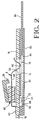
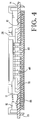
- an electrical connector is shown generally at 2 comprising a fixed housing portion 4, a rotatable housing portion 6 pivotally connected to the housing portion 4, and a plurality of electrical terminals such as 8.
- the housing portion 4 includes mounting flanges 10 at each end, the flanges 10 including a lower mounting surface 12 for abutment against a printed circuit board such as 14 shown in Figure 4.
- Latches 16 extend from each end part of the flanges 10 and further include latches 18 extending from the rear side of the connector housing 4.
- each of the latching arms 16 and 18 include engaging portions 20 for securing the connector 2 to the printed circuit board 14.
- the rotatable housing 6 includes two camming legs 24 which span the contacts 8 and extend downwardly through the printed circuit board as best shown in Figure 2.
- the camming legs have forwardly facing camming edges 25.
- the housing 4 includes pivot blocks such as 26 having internal cylindrical openings 28 as shown in phantom in Figure 1, and the rotatable housing portions 6 includes pivot pins 30 positioned in the openings 28.
- the openings 28 and pivot pins 30 would be profiled for a close tolerance fit, the aperture 28 is shown larger than the pin 30 in Figure 1 for clarity only.
- an engaging section 32 extends forwardly from front edge 34 of the rotatable housing portion 6 and as shown in Figure 2 includes an engaging lip 36 which would be described in greater detail herein.
- the connector includes a central body portion shown generally at 40 which houses the plurality of electrical terminals 8, and in the preferred embodiment of the invention, the terminals 8 are integrally molded within the central body portion 40.
- the terminals are stamped and formed to include a rear surface mount portion 42 and a forward cantilever beam portion 44 having a formed U-shaped contact portion 46.
- the printed circuit board 14 includes a formed rectangular opening 50, two rectangular openings 52, mounting apertures 56 and 58, centering apertures 60, and a plurality of conductive traces such as 62.
- the assembly also includes a card receiving tray 65 which can be mounted to the lower surface of the printed circuit board 14.
- the tray 65 includes a card receiving guide 66 having a rear edge 67, and channels 68 which extend from an upper surface 70 of the trade and communicate with the guide 66.
- the tray 65 further includes an opening 72 which in the preferred embodiment, would be the same configuration as the rectangular opening 50 in the printed circuit board 14.
- the tray 65 can be installed to the lower surface of the printed circuit board 14 such that the openings 72 and 50 are in alignment as shown in Figure 2, and such that the openings 52 through the printed circuit board overlay the channel 68 in card guide 65. It should be appreciated that location members such as pegs will be incorporated into the card guide 65 to locate the card guide relative to the printed circuit board. Also, although not specifically shown, the card tray 65 will include some means of being retained to lower surface of the printed circuit board 14.
- the connector 2 can now be positioned on the top surface of the printed circuit board 14 with the surface mount portions 42 positioned over respective traces 62 and with the contact portions 46 positioned in the opening 50 of the printed circuit board and partially extending into the opening 72 of the card guide as shown in Figure 2.
- latching members 16 are profiled to latch within apertures 56 in the printed circuit board while latching members 18 are profiled for receipt within the apertures 58.
- Camming legs 24 extend downwardly through the rectangular openings 52 in the printed circuit board into the channel 68 of the card guide, such that the camming surfaces 25 of the camming legs 24 face forwardly towards the card receiving slide 66.
- the cantilever beam portions 44 of the terminals 8 are sprung upwardly somewhat, such that the contact surfaces of the U-shaped contact portions 46 are above the upper surface 76 of the card receiving guide 65.
- a memory card or so-called smart card is shown generally at 80 and includes a plurality of electrical traces 82.
- the card 80 can be inserted as shown in Figure 2 where the card is received in the card receiving guide 66 and can be pushed forward toward the camming legs 24. With the connector in the position shown in Figure 2, the card will pass beneath contact portions 46 without contacting them.
- the memory card 80 causes the leading edge 84 to engage surfaces 25 and pivot the rotating housing member 6 in the clockwise sense, as viewed in Figure 2. This rotation causes the lip portion 36 to engage the cantilever beam portions 44 of the terminals 8, thereby forcing the contact portions 46 against the electrical traces 82 on the memory card 80.
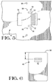
- the distance L as shown in Figure 3 which corresponds to the distance from the back surface 69 of the channel 68 to the center of the contact portions 46, also corresponds to the distance L shown Figure 6, that is the distance between the leading edge 84 and the center of the traces 82.
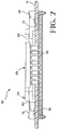
- Figure 7 shows an alternate embodiment of the connector of Figures 1-6, where the connector 102 has a housing portion 104 and a rotatable housing portion 106.
- a tray portion 165 is positioned below the board similarly to the former embodiment.
- the latches 16, 18 of the previous embodiment are removed, and the housing 104 and the tray portion 165 are held together, with the board 14 sandwiched in between by way of fasteners such as screws 130.
Applications Claiming Priority (2)
| Application Number | Priority Date | Filing Date | Title |
|---|---|---|---|
| GB9202313A GB9202313D0 (en) | 1992-02-04 | 1992-02-04 | Smart card connector |
| GB9202313 | 1992-02-04 |
Publications (2)
| Publication Number | Publication Date |
|---|---|
| EP0554821A1 true EP0554821A1 (fr) | 1993-08-11 |
| EP0554821B1 EP0554821B1 (fr) | 1998-05-20 |
Family
ID=10709778
Family Applications (1)
| Application Number | Title | Priority Date | Filing Date |
|---|---|---|---|
| EP19930101527 Expired - Lifetime EP0554821B1 (fr) | 1992-02-04 | 1993-02-01 | Connecteur pour carte à puce |
Country Status (4)
| Country | Link |
|---|---|
| EP (1) | EP0554821B1 (fr) |
| JP (1) | JPH05283132A (fr) |
| DE (1) | DE69318589T2 (fr) |
| GB (1) | GB9202313D0 (fr) |
Cited By (5)
| Publication number | Priority date | Publication date | Assignee | Title |
|---|---|---|---|---|
| WO1995023385A1 (fr) * | 1994-02-28 | 1995-08-31 | General Instrument Corporation Of Delaware | Boite de conversion de canaux de television par cable, avec connecteur de carte a puce situe sous la boite |
| EP0746062A2 (fr) * | 1995-06-02 | 1996-12-04 | Molex Incorporated | Connecteur électrique engageable en surface |
| WO1998039724A2 (fr) * | 1997-03-06 | 1998-09-11 | Siemens Aktiengesellschaft | Prise femelle pour mise en contact d'au moins une surface de contact dans une surface d'un element enfichable |
| GB2346016A (en) * | 1998-12-07 | 2000-07-26 | Whitaker Corp | Smart card connector with card detection switch |
| WO2011081822A2 (fr) * | 2009-12-14 | 2011-07-07 | Fci | Connecteur pour carte à puce |
Families Citing this family (5)
| Publication number | Priority date | Publication date | Assignee | Title |
|---|---|---|---|---|
| US7811100B2 (en) | 2007-07-13 | 2010-10-12 | Fci Americas Technology, Inc. | Electrical connector system having a continuous ground at the mating interface thereof |
| US8764464B2 (en) | 2008-02-29 | 2014-07-01 | Fci Americas Technology Llc | Cross talk reduction for high speed electrical connectors |
| US9277649B2 (en) | 2009-02-26 | 2016-03-01 | Fci Americas Technology Llc | Cross talk reduction for high-speed electrical connectors |
| US8267721B2 (en) | 2009-10-28 | 2012-09-18 | Fci Americas Technology Llc | Electrical connector having ground plates and ground coupling bar |
| KR101977616B1 (ko) * | 2018-11-27 | 2019-05-13 | 에스씨에스프로 주식회사 | 양방향 랜딩 방식의 ic 카드 소켓 |
Citations (3)
| Publication number | Priority date | Publication date | Assignee | Title |
|---|---|---|---|---|
| EP0399763A2 (fr) * | 1989-05-23 | 1990-11-28 | Hitachi Maxell Ltd. | Dispositif de lecture et d'écriture d'une carte à circuit intégré |
| EP0468828A1 (fr) * | 1990-07-23 | 1992-01-29 | Itt Composants Et Instruments | Connecteur électrique pour cartes à mémoire électronique |
| EP0482548A1 (fr) * | 1990-10-25 | 1992-04-29 | Alcatel Cit | Cadre de contact pour lecteur de carte à puce |
-
1992
- 1992-02-04 GB GB9202313A patent/GB9202313D0/en active Pending
-
1993
- 1993-01-27 JP JP5029598A patent/JPH05283132A/ja active Pending
- 1993-02-01 DE DE1993618589 patent/DE69318589T2/de not_active Expired - Fee Related
- 1993-02-01 EP EP19930101527 patent/EP0554821B1/fr not_active Expired - Lifetime
Patent Citations (3)
| Publication number | Priority date | Publication date | Assignee | Title |
|---|---|---|---|---|
| EP0399763A2 (fr) * | 1989-05-23 | 1990-11-28 | Hitachi Maxell Ltd. | Dispositif de lecture et d'écriture d'une carte à circuit intégré |
| EP0468828A1 (fr) * | 1990-07-23 | 1992-01-29 | Itt Composants Et Instruments | Connecteur électrique pour cartes à mémoire électronique |
| EP0482548A1 (fr) * | 1990-10-25 | 1992-04-29 | Alcatel Cit | Cadre de contact pour lecteur de carte à puce |
Cited By (9)
| Publication number | Priority date | Publication date | Assignee | Title |
|---|---|---|---|---|
| WO1995023385A1 (fr) * | 1994-02-28 | 1995-08-31 | General Instrument Corporation Of Delaware | Boite de conversion de canaux de television par cable, avec connecteur de carte a puce situe sous la boite |
| EP0746062A2 (fr) * | 1995-06-02 | 1996-12-04 | Molex Incorporated | Connecteur électrique engageable en surface |
| EP0746062A3 (fr) * | 1995-06-02 | 1998-11-04 | Molex Incorporated | Connecteur électrique engageable en surface |
| WO1998039724A2 (fr) * | 1997-03-06 | 1998-09-11 | Siemens Aktiengesellschaft | Prise femelle pour mise en contact d'au moins une surface de contact dans une surface d'un element enfichable |
| WO1998039724A3 (fr) * | 1997-03-06 | 1998-12-10 | Siemens Ag | Prise femelle pour mise en contact d'au moins une surface de contact dans une surface d'un element enfichable |
| GB2346016A (en) * | 1998-12-07 | 2000-07-26 | Whitaker Corp | Smart card connector with card detection switch |
| GB2346016B (en) * | 1998-12-07 | 2002-11-13 | Whitaker Corp | Smart card connector with card detection switch |
| WO2011081822A2 (fr) * | 2009-12-14 | 2011-07-07 | Fci | Connecteur pour carte à puce |
| WO2011081822A3 (fr) * | 2009-12-14 | 2011-10-27 | Fci | Connecteur pour carte à puce |
Also Published As
| Publication number | Publication date |
|---|---|
| JPH05283132A (ja) | 1993-10-29 |
| DE69318589T2 (de) | 1998-11-19 |
| DE69318589D1 (de) | 1998-06-25 |
| EP0554821B1 (fr) | 1998-05-20 |
| GB9202313D0 (en) | 1992-03-18 |
Similar Documents
| Publication | Publication Date | Title |
|---|---|---|
| EP0650230B1 (fr) | Loquet pour connecteur électrique | |
| US5026291A (en) | Board mounted connector system | |
| EP0520080B1 (fr) | Connecteur pour des cartes à puce | |
| US5211568A (en) | Edge card connector with latch/eject mechanism | |
| US5184961A (en) | Modular connector frame | |
| US5207598A (en) | Edge card connector | |
| US5046955A (en) | Active connector assembly | |
| US5277627A (en) | Electrical connector for IC card | |
| US5199895A (en) | Low insertion force, self-locking connecting apparatus for electrically connecting memory modules to a printed circuit board | |
| JPH0613117A (ja) | 電気コネクタ | |
| KR100286566B1 (ko) | 전기 커넥터 | |
| EP0923796A2 (fr) | Connecteur acceptant un carte miniature | |
| US5520551A (en) | Molded latching apparatus for printed circuit mounted components | |
| EP0554821A1 (fr) | Connecteur pour carte à puce | |
| US5354216A (en) | Mounting system for electrical connectors | |
| US5188534A (en) | Surface mount connector with clip engaging contacts | |
| US5531615A (en) | Coplanar computer docking apparatus | |
| US6447313B1 (en) | IC card connector | |
| US6626685B2 (en) | Card connector cover and card connector assembly | |
| US6112994A (en) | Card reader connector with attachable cover | |
| US20040242040A1 (en) | Card connector with locking device | |
| CN216903566U (zh) | 按压组件及其连接器 | |
| US20010027045A1 (en) | Electrical connector system | |
| US6340307B1 (en) | Electrical connector | |
| JPH09213433A (ja) | 高速および高密度の接触ストリップを備えた電気的コネクタ |
Legal Events
| Date | Code | Title | Description |
|---|---|---|---|
| PUAI | Public reference made under article 153(3) epc to a published international application that has entered the european phase |
Free format text: ORIGINAL CODE: 0009012 |
|
| AK | Designated contracting states |
Kind code of ref document: A1 Designated state(s): DE GB NL |
|
| 17P | Request for examination filed |
Effective date: 19940210 |
|
| 17Q | First examination report despatched |
Effective date: 19960701 |
|
| GRAG | Despatch of communication of intention to grant |
Free format text: ORIGINAL CODE: EPIDOS AGRA |
|
| GRAG | Despatch of communication of intention to grant |
Free format text: ORIGINAL CODE: EPIDOS AGRA |
|
| GRAH | Despatch of communication of intention to grant a patent |
Free format text: ORIGINAL CODE: EPIDOS IGRA |
|
| GRAH | Despatch of communication of intention to grant a patent |
Free format text: ORIGINAL CODE: EPIDOS IGRA |
|
| GRAA | (expected) grant |
Free format text: ORIGINAL CODE: 0009210 |
|
| AK | Designated contracting states |
Kind code of ref document: B1 Designated state(s): DE GB NL |
|
| REF | Corresponds to: |
Ref document number: 69318589 Country of ref document: DE Date of ref document: 19980625 |
|
| PGFP | Annual fee paid to national office [announced via postgrant information from national office to epo] |
Ref country code: NL Payment date: 19981222 Year of fee payment: 7 |
|
| PLBE | No opposition filed within time limit |
Free format text: ORIGINAL CODE: 0009261 |
|
| STAA | Information on the status of an ep patent application or granted ep patent |
Free format text: STATUS: NO OPPOSITION FILED WITHIN TIME LIMIT |
|
| 26N | No opposition filed | ||
| PGFP | Annual fee paid to national office [announced via postgrant information from national office to epo] |
Ref country code: GB Payment date: 19991224 Year of fee payment: 8 |
|
| PGFP | Annual fee paid to national office [announced via postgrant information from national office to epo] |
Ref country code: DE Payment date: 19991229 Year of fee payment: 8 |
|
| PG25 | Lapsed in a contracting state [announced via postgrant information from national office to epo] |
Ref country code: NL Free format text: LAPSE BECAUSE OF NON-PAYMENT OF DUE FEES Effective date: 20000901 |
|
| NLV4 | Nl: lapsed or anulled due to non-payment of the annual fee |
Effective date: 20000901 |
|
| PG25 | Lapsed in a contracting state [announced via postgrant information from national office to epo] |
Ref country code: GB Free format text: LAPSE BECAUSE OF NON-PAYMENT OF DUE FEES Effective date: 20010201 |
|
| GBPC | Gb: european patent ceased through non-payment of renewal fee |
Effective date: 20010201 |
|
| PG25 | Lapsed in a contracting state [announced via postgrant information from national office to epo] |
Ref country code: DE Free format text: LAPSE BECAUSE OF NON-PAYMENT OF DUE FEES Effective date: 20011201 |